
Polyhedron Cu2O@Ag composite microstructures: synthesis, mechanism analysis and structure-dependent SERS properties
Haiqing Luoa,
Jun Zhou*a,
Hanhua Zhonga,
Lu Zhoua,
Zhenghong Jiab and
Xiaoling Tanc
aInstitute of Photonics, Faculty of Science, Ningbo University, Ningbo, 315211, Zhejiang, China. E-mail: zhoujun@nbu.edu.cn; Fax: +86-574-87600744; Tel: +86-574-87600794
bSchool of Information Science and Engineering, Xinjiang University, Urumqi, 830046, Xinjiang, China
cSchool of Electronics and Communication, Shenzhen Institute of Information Technology, Shenzhen, 518172, Guangdong, China
First published on 7th October 2016
Abstract
Composite microstructures consisting of Cu2O polyhedrons and Ag nanoparticles (Cu2O@Ag CMs) were successfully prepared through a modified reduction method. In the synthesis process of the Cu2O crystals, by modulating the concentrations of surfactant poly(vinyl pyrrolidone), the as-prepared Cu2O polyhedrons with diverse morphologies displayed a unique shape evolution which clearly revealed their growth mechanism. By in situ adding AgNO3 into the Cu2O solution, Cu2O@Ag CMs were synthesized and their surface-enhanced Raman scattering (SERS) performances were evaluated with the help of labeling with 4-mercaptobenzoic acid molecules. The experimental and simulated results shown that the Cu2O@Ag CMs exhibit structure-dependent SERS characteristics, i.e., their SERS enhancements closely relied on the morphologies of the Cu2O polyhedrons, and the sizes and distributions of the Ag nanoparticles. Especially, under the optimized synthesis conditions, the as-prepared concave trisoctahedron Cu2O@Ag CMs have a superior SERS activity with an enhancement factor of 3.21 × 10⁶. This shows that the synthesized Cu2O@Ag CMs could have potential applications in chemical and biological fields.
1 Introduction
Over the past few decades, the development of novel surface-enhanced Raman scattering (SERS) technology has induced increasing attention for applications in supersensitive detection and identification of chemical or biological species.1–3 As typical SERS materials, the noble metals such as Au, Ag and Cu are generally used to fabricate SERS substrates for their unique surface plasmon resonance (SPR) properties.4 However, owing to the high surface energies of the noble metal nanoparticles (NPs), particularly Ag NPs, they are prone to aggregation during the assembly process of SERS substrates, so there is a severe challenge to obtain homogeneous SERS substrates with higher enhancement activity in practical applications.5 To avoid the agglomeration of Ag NPs, some elaborate methods have been proposed to synthesize monodisperse microstructures, such as Ag micro-hemispheres and Ag hollow microcubes assembled from nanosheets, to serve as excellent SERS substrates due to the abundant active “hot spots” on their surfaces.6,7 Recently, much effort has been devoted to designing and preparing SERS substrates with excellent performance using various composites of semiconductors and noble metal NPs. For example, TiO2@Ag nanofibers were prepared by an electrospinning technique and reduction method and used to fabricate SERS substrates with a stable Raman signal.8 The Shivaprasad group demonstrated a SERS substrate consisting of a GaN nanowall network structure and Ag nanodroplets which exhibited higher SERS enhancement.9 By a hydrothermal approach and magnetron sputtering, our group also fabricated a SERS substrate of α-MnO2 nanorods attached to Au NPs and explored its ideal SERS application for biosensing.10 In fact, the SERS effect of the above materials can be attributed to the electromagnetic enhancement of noble metal NPs and the chemical enhancement of the semiconductor.11 Therefore, it is worth preparing metal–semiconductor hybrid structures and studying their high SERS enhancement dependence on the morphologies of the semiconductor and noble metal NPs simultaneously.As well known, as a p-type semiconductor material, Cu2O is both inexpensive and non-poisonous, especially, its narrow bandgap (1.9–2.2 eV) matches the visible spectrum well and is suitable for wide potential applications.12,13 It is due to the above benefits that much work has been focused on the synthesis of Cu2O crystals with various morphologies, such as spheres,14 cubes,15 hierarchical structures,16,17 and branched shapes.18–20 And this work has demonstrated that the final stable morphologies of Cu2O crystals are very important for their properties and applications. In fact, during the synthesis process, Cu2O crystals with a variety of morphologies can be obtained by fine tuning the reaction conditions in which the organic additives play a key role in stabilizing the crystal facets of Cu2O.21 So, to further understand the growth mechanism of Cu2O, it is interesting to systematically study the relationship of Cu2O morphology and reaction conditions such as the concentration of surfactant. On the other hand, there were many studies about the preparation of Cu2O@metal composites (CMs) for their catalysis and gas sensing applications.22–24 However, only a few Cu2O@metal composites were reported as SERS active substrates.25 To our knowledge, the visible-light absorption band of Cu2O has an overlap with the localized surface plasmonic resonance (LSPR) peak of noble metal nanoparticles, which could induce a high SERS effect by electromagnetic enhancement.26 At the same time, as an effective plasmonic material, Ag has good Raman enhancement ability. After the deposition of Ag NPs onto the surface of Cu2O, the charges in the Cu2O@Ag composite are redistributed, which results in the high charge density region located adjacent to the interface of metal–semiconductor due to the electron transfer between Ag and Cu2O.27 It is the high charge density which produces an enhanced electromagnetic field and excites an intense LSPR under irradiation with a suitable laser. Therefore, it is expected that the Cu2O@Ag composite will exhibit excellent SERS behavior and be a SERS active substrate with high sensitivity and stability.
In this paper, micrometer-sized Cu2O polyhedrons with different shapes were synthesized by a simple reduction approach under optimal reaction conditions. By varying the amount of surfactant, the morphologies of Cu2O polyhedrons evolved from a flower with eight petals, cube with missing angles, truncated octahedron, truncated concave trisoctahedron, concave trisoctahedron to octahedron. And based on the presenting of growth rates of the different crystal facets, the unique morphologic evolution of Cu2O polyhedrons was analyzed to reveal their possible formation mechanism. Moreover, the composites of Cu2O polyhedron and Ag nanoparticles were prepared by in situ adding AgNO3 into Cu2O solutions, and their SERS performances were investigated experimentally. And the structure-dependent SERS enhanced characteristics of the as-prepared Cu2O@Ag CMs have been analyzed using the finite element method (FEM) in detail. Furthermore, it is found that the concave trisoctahedron Cu2O@Ag CM exhibits a higher SERS enhancement and the calculated enhancement factor presents a superior advantage for SERS applications.
2 Experimental
2.1 Chemicals
Hydrous copper sulfate (CuSO4·5H2O), anhydrous sodium carbonate (Na2CO3), glucose, and poly(vinyl pyrrolidone) (PVP, MW 30![[thin space (1/6-em)]](https://www.rsc.org/images/entities/char_2009.gif) 000) were purchased from Sinopharm Chemical Reagent Co., Ltd. AgNO3 was purchased from Sigma-Aldrich. Trisodium citrate (Na3C6H5O7·2H2O) was purchased from Bodi Chemical Reagent Co., Ltd. (Tianjin, China). 4-Mercaptobenzoic acid (4MBA) was obtained from J&K Chemical. Milli-Q water (18.2 MΩ cm resistivity) was used for all solution preparation. Glassware was cleaned using aqua regia and rinsed with deionized water several times before the experiments.
000) were purchased from Sinopharm Chemical Reagent Co., Ltd. AgNO3 was purchased from Sigma-Aldrich. Trisodium citrate (Na3C6H5O7·2H2O) was purchased from Bodi Chemical Reagent Co., Ltd. (Tianjin, China). 4-Mercaptobenzoic acid (4MBA) was obtained from J&K Chemical. Milli-Q water (18.2 MΩ cm resistivity) was used for all solution preparation. Glassware was cleaned using aqua regia and rinsed with deionized water several times before the experiments.
2.2 Synthesis of the Cu2O crystals
In our experiments, a varies of polyhedral Cu2O crystals were synthesized using a modified reduction method.27 The synthesis process of Cu2O crystals is presented as follows. Firstly, the solutions of CuSO4 (0.0358 M), Na2CO3 (800 μL, 1.2 M) and Na3C6H5O7 (800 μL, 0.74 M) were prepared using deionized water under vigorous stirring for 10 min. Then, 7.6 mL of CuSO4 solution was slowly added to the mixed salt solution of Na2CO3 (800 μL) and Na3C6H5O7 (800 μL) with fierce shaking for uniform dispersion. Subsequently, a certain amount of PVP (MW = 30000) was added into the above solution under stirring for 30 min. After full dissolving of PVP, 400 μL of 1.4 M glucose solution was slowly dropped into the mixture solution. Finally, the mixture solution was kept in a water bath at a temperature of 80 °C for 15 min, then the color of the mixture solution changed from deep blue to brick red and the Cu2O crystals were obtained.
Furthermore, for the above synthesis process, the morphologies of the as-prepared Cu2O polyhedrons can be controlled by varying the concentrations of surfactant. In our experiments, with tuning the concentrations of PVP (0, 0.33, 1.0, 1.67, 2.33, and 5 mM), six types of polyhedral Cu2O crystals were synthesized and were to be used as the Cu2O-containing mother solutions.
2.3 Synthesis of the Cu2O@Ag CMs
Firstly, each of the above Cu2O-containing mother solutions was divided into five equal parts. Then the different amounts of AgNO3 solutions (50, 100, 200, 300 and 500 μL) with a concentration of 0.01 M were added into the five equal amounts of Cu2O mother solutions (2 mL) under stirring for 30 min. The colors of the reaction solutions changed from brick-red to deep gray, which suggests the uniform Cu2O@Ag CMs were formed. Next, the Cu2O@Ag CMs solutions were purified by centrifuging at 3000 rpm for 5 min and the sediments were dispersed in 2 mL of deionized water as sample solutions. Lastly, for all of the as-synthesized Cu2O@Ag CMs, 30 sample solutions were obtained and stored to be used in later experiments.2.4 Synthesis of the 4MBA-labelled Cu2O@Ag CMs
The SERS performances of the as-synthesized Cu2O@Ag CMs were evaluated with 4MBA Raman molecules. Firstly, 20 μL of 10 mM 4MBA solutions were respectively added into 1 mL of the above Cu2O@Ag CMs sample solutions under stirring, and the resultant solutions were agitated by magnetic stirring for 5 h. Then, the mixtures were centrifuged at 3000 rpm for 5 min to remove unbound 4MBA molecules. Afterwards, the sediments at the bottom of the centrifuge tubes were dispersed in 2 mL of deionized water as 4MBA-labelled Cu2O@Ag CMs solutions for SERS measurement.2.5 Instrumentation and measurements
The UV-Vis-NIR absorption spectra were monitored with a spectrometer (Cary 5000, Agilent). The scanning electron microscopy (SEM) images were recorded using a field emission SEM (SU-70, Hitachi) under an accelerating voltage of 5 kV. The X-ray diffraction (XRD) patterns were measured using an X-ray powder diffractometer (Ru-200b, Rigaku) with nickel-filtered Cu-Kα radiation (λ = 1.540630 Å) for identifying the phase structures of the products. Transmission electron microscope (TEM) images and selective area electron diffraction (SAED) patterns were obtained with a TEM (JEM-2100F, JEOL) operating at an accelerating voltage of 200 kV. The SERS properties of the samples were examined using a Raman spectrometer (BWS415, B&W Tek) with specifications as follows: a 785 nm semiconductor laser as the excitation source and laser power of 49.55 mW in 10 s; a 40× objective lens with numerical aperture (NA) of 0.65 to focus the laser beam; the wavelength dispersion was performed using a 1200 lines per mm grating, and then passed through a slit with 20 mm width to the charge-coupled device (CCD) (2048 × 2048 pixels) detector. All the measurements were carried out at room temperature.3 Results and discussion
3.1 Characterization of the polyhedral Cu2O
According to the description in Section 2.2, a series of Cu2O crystals with different morphologies were synthesized by changing the concentrations of surfactant. And the SEM images of six types of as-prepared Cu2O crystals are shown in Fig. 1. From Fig. 1, the uniformities of these Cu2O crystals are very good and their shape evolution was clearly shown by simply increasing the PVP concentration. As seen in Fig. 1(a), the flower Cu2O crystals with eight petals were obtained for the case without surfactant. The missing angles cube crystals can be observed in Fig. 1(b) for the PVP concentration of 0.33 mM. And the truncated octahedron crystals shown in Fig. 1(c) were produced with increasing the concentration of PVP to 1.0 mM. Upon further increasing the concentration of PVP from 1.67 mM to 2.33 mM, the truncated concave trisoctahedron Cu2O crystals and the concave trisoctahedron Cu2O crystals were synthesized and are shown in Fig. 1(d) and (e), respectively. Eventually, at the PVP concentration of 5 mM, the octahedron Cu2O crystals were obtained and are shown in Fig. 1(f). It was concluded that the morphology of the as-synthesized Cu2O crystals strongly relies on the amount of surfactant.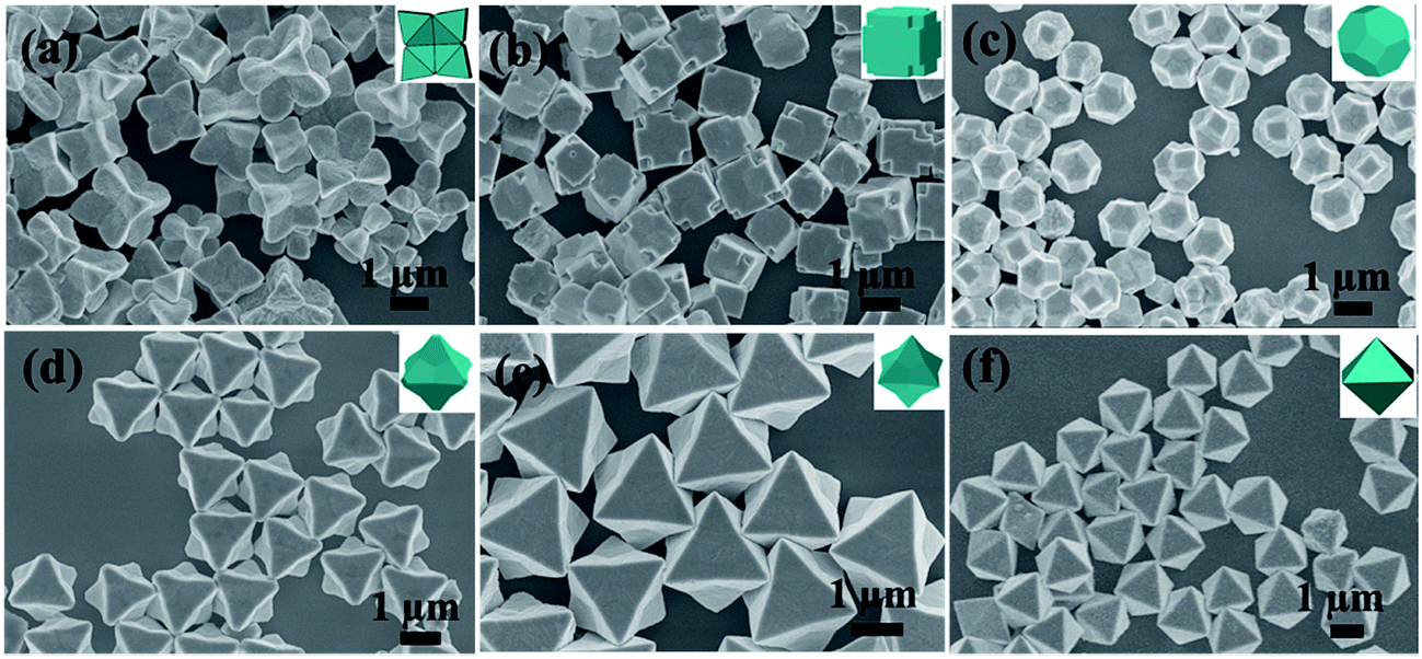 | ||
| Fig. 1 SEM images of as-synthesized Cu2O crystals of (a) flower with eight petals, (b) missing angles cube, (c) truncated octahedron, (d) truncated concave trisoctahedron, (e) concave trisoctahedron, and (f) octahedron. The insets show the corresponding drawings of the respective geometric morphologies. | ||
Fig. 2 presents the TEM images of Cu2O crystals with various morphologies and their corresponding SAED patterns. It can be found that the Cu2O crystals are single crystalline microstructures with sharp profile faces. In Fig. 2(a1), the edge portion of Cu2O crystals exhibits a well-defined flower with eight petals of an average diagonal size of 2.08 ± 0.05 μm. The missing angles cubes shown in Fig. 2(b1) have an average diagonal size of 1.58 ± 0.07 μm. The spacing of opposite facets of the truncated octahedron and the truncated concave trisoctahedron displayed in Fig. 2(c1) and (d1) are about 1.75 ± 0.10 μm and 2.15 ± 0.12 μm, respectively. In Fig. 2(e1), the concave trisoctahedron shows a smooth curvature for its branches and the diagonal size is about 2.21 ± 0.15 μm. And, from Fig. 2(f1), the diagonal size of the octahedron is about 2.46 ± 0.16 μm. The SAED patterns are shown in Fig. 2(a2)–(f2), which presents that all of the Cu2O crystals are single crystals. In addition, the XRD patterns corresponding to all the Cu2O crystals are shown in Fig. 2(a3)–(f3). From these XRD patterns, it is found that, with the morphologic changes of Cu2O crystals, the intensities of the (111) peaks increase progressively and the intensities of the (200) peaks decrease distinctly. The observed relative transition between the intensities of the (111) and (200) peaks may come from the result of the dominant lattice plane and the preferred orientation of crystals deposited on the substrates.28 As two typical examples, the missing angles cube shows an exceptionally strong (200) peak and an extremely weak (111) peak, but the octahedron shows the opposite case. Especially, comparing with other crystals, the intensity of the (111) peak of the concave trisoctahedron is abnormally high and even exceeds that of the octahedron due to its numerous lattice planes.
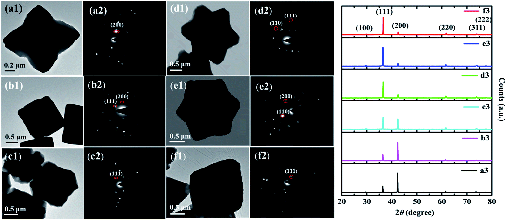 | ||
| Fig. 2 TEM images of the Cu2O crystals with the morphologies: (a1) the flower with eight petals, (b1) the missing angles cube, (c1) the truncated octahedron, (d1) the truncated concave trisoctahedron, (e1) the concave trisoctahedron, and (f1) the octahedron. The SAED patterns corresponding to the Cu2O crystals are shown in (a2–f2), and their corresponding XRD patterns are recorded in (a3–f3). In all XRD patterns, the intensities of peaks are the relative intensity with the same intensity scale. | ||
3.2 Growth mechanism of polyhedron Cu2O
As shown in Fig. 3, the synthesis process for the Cu2O crystals can be simply concluded as follows: to start with, the sodium mixture was added into the copper sulfate solution to prepare the copper citrate, then the glucose as a reducing agent was added into the reaction solution to form Cu2O crystals with the help of the surfactant PVP, and finally the polyhedron Cu2O with different morphologies were obtained by changing the concentration of PVP. In the above process, the amounts of sodium mixture and PVP are affirmed to play key roles to determine the final shape of the Cu2O crystals. First, the sodium mixture serves as the chelating ligand to form copper citrate and the amount of sodium mixture determines the pH environment of the copper citrate solution that affects the reaction rates.29 Second, as a typical surfactant, the amount of PVP has great influence on the shape and surface structure of the Cu2O crystals. As is well known, the surface energies of the low-index crystallographic facets of Cu2O crystals are given in the order of γ {100} < γ {111} < γ {110}, so that the final shape and geometry of the nanocrystals relies on the distribution of exposed crystallographic facets by promoting selective growth in certain crystallographic directions.30,31 For the electrostatic molding of a specific facet, the negatively charged O atoms in the C![[double bond, length as m-dash]](https://www.rsc.org/images/entities/char_e001.gif) O of PVP would strongly interact with the positively charged dangling Cu atoms on the {111} facet of the crystal to stabilize the crystal surfaces and inhibit the growth rate of {111}. It is the capping and stabilizing role of PVP to make the dissociative particles be close-packed on the most thermodynamically favored facets of the crystal with different growth rates so that the as-synthesized Cu2O crystal is grown by the ratio R of the growth rates of the 〈100〉 direction to that of the 〈111〉 direction.32 That is, there is a positive correlation between R and the amount of PVP and the ratio of the surface area of {111} to that of {100} could be modified by varying the amount of PVP. For the case of no PVP participating, the as-synthesized Cu2O crystal (R < 0.7) has the shape of a flower with eight petals and exposes the {100} facets with the lowest energies. When small quantities of PVP (0.33 mM) were added into the reaction solution, the missing angles cube (R ≈ 0.7) tends to show the {100} facets due to the weaker or insufficient capping effect of PVP, which is similar to the case of no PVP but decreases the occupancy area of the {100} facets.29 With the increasing of PVP concentration, the capping effect of PVP would prevent the atoms from stacking on the {111} facets and facilitate the growth on the {100} facets. It could be believed that the greatly enhanced inhibition of PVP at 1 mM is responsible for the formation of the truncated octahedron with a value of R ≈ 1.33 When the PVP concentration is further increased, the growth rates of the {100} facets and that of the {111} facets are obviously different and the value R will change in the range of 1 < R < 1.73. For example, at two high concentrations of PVP such as 1.67 and 2.33 mM, the energy of the {100} facet is declined and the growth is taken along the [100] direction, which results in the formation of the truncated concave trisoctahedron and the concave trisoctahedron, respectively. As shown in Fig. 2(d1), except for the 6 truncated {100} facets, the 24 exposed inclined surfaces of the truncated concave trisoctahedron are the {111} facets. With the disappearance of the {100} facets, the as-prepared concave trisoctahedron is fully enclosed by the 24 exposed {111} facets. Furthermore, at the extremely high concentration, 5 mM of PVP, the perfect octahedron is obtained at a maximum ratio R = 1.73 owing to the PVP being covered on all the {111} facets of the Cu2O crystals. In fact, other synthesis conditions, such as the concentration of glucose, temperature and reaction time have effects on the shapes of Cu2O crystals, which will be investigated in our later experiments.34–36
O of PVP would strongly interact with the positively charged dangling Cu atoms on the {111} facet of the crystal to stabilize the crystal surfaces and inhibit the growth rate of {111}. It is the capping and stabilizing role of PVP to make the dissociative particles be close-packed on the most thermodynamically favored facets of the crystal with different growth rates so that the as-synthesized Cu2O crystal is grown by the ratio R of the growth rates of the 〈100〉 direction to that of the 〈111〉 direction.32 That is, there is a positive correlation between R and the amount of PVP and the ratio of the surface area of {111} to that of {100} could be modified by varying the amount of PVP. For the case of no PVP participating, the as-synthesized Cu2O crystal (R < 0.7) has the shape of a flower with eight petals and exposes the {100} facets with the lowest energies. When small quantities of PVP (0.33 mM) were added into the reaction solution, the missing angles cube (R ≈ 0.7) tends to show the {100} facets due to the weaker or insufficient capping effect of PVP, which is similar to the case of no PVP but decreases the occupancy area of the {100} facets.29 With the increasing of PVP concentration, the capping effect of PVP would prevent the atoms from stacking on the {111} facets and facilitate the growth on the {100} facets. It could be believed that the greatly enhanced inhibition of PVP at 1 mM is responsible for the formation of the truncated octahedron with a value of R ≈ 1.33 When the PVP concentration is further increased, the growth rates of the {100} facets and that of the {111} facets are obviously different and the value R will change in the range of 1 < R < 1.73. For example, at two high concentrations of PVP such as 1.67 and 2.33 mM, the energy of the {100} facet is declined and the growth is taken along the [100] direction, which results in the formation of the truncated concave trisoctahedron and the concave trisoctahedron, respectively. As shown in Fig. 2(d1), except for the 6 truncated {100} facets, the 24 exposed inclined surfaces of the truncated concave trisoctahedron are the {111} facets. With the disappearance of the {100} facets, the as-prepared concave trisoctahedron is fully enclosed by the 24 exposed {111} facets. Furthermore, at the extremely high concentration, 5 mM of PVP, the perfect octahedron is obtained at a maximum ratio R = 1.73 owing to the PVP being covered on all the {111} facets of the Cu2O crystals. In fact, other synthesis conditions, such as the concentration of glucose, temperature and reaction time have effects on the shapes of Cu2O crystals, which will be investigated in our later experiments.34–36
 | ||
| Fig. 3 The schematic of the growth mechanism of the polyhedron Cu2O. | ||
3.3 SERS performance of the polyhedral Cu2O@Ag CMs
With the aim of investigating the SERS properties of the composites of Cu2O and Ag NPs, the 4MBA-labelled Cu2O@Ag CMs solutions prepared in Section 2.4 were dropped onto Si wafers for measuring of their respective SERS spectra. And all the SERS spectra of the 4MBA-labelled Cu2O@Ag CMs are shown in Fig. 4. As shown in Fig. 4(a)–(e), the two dominant peaks at 1077 and 1590 cm−1 are assigned to the ring-breathing modes of 4MBA molecules, and their intensities are obviously different for the different Cu2O@Ag structures.37 To illustrate clearly the structure-dependent SERS characteristics of the Cu2O@Ag CMs, the peak intensities of 1077 cm−1 are plotted in Fig. 4(f) as varying with the volumes of the AgNO3 solutions. From Fig. 4(f), the SERS intensities are found to be increased with increasing volumes of AgNO3 solutions, and there are maximums at 300 μL of AgNO3 solution for three Cu2O@Ag CMs with underlying concave structures, including the flower with eight petals, the truncated concave trisoctahedron and the concave trisoctahedron. On the other hand, in a low content of AgNO3 such as 50 μL, the truncated concave trisoctahedron, the concave trisoctahedron and the octahedron perform superior SERS behaviors. However, for the Cu2O@Ag CMs with the concave structure of a flower with eight petals, there is a lower SERS enhancement compared with that of the Cu2O@Ag CMs with the concaved trisoctahedron or the sharp-angled octahedron, owing to the eight petals with blunt corners rather than sharp corners. And, in the case of high content of AgNO3 at 500 μL, the concave trisoctahedron with concave and sharp corners still performs with better SERS behavior compared with the other structures. Thus, the Cu2O polyhedrons with concave faces and/or sharp corners are speculated as the superior structures to enhance SERS activity besides the role of the Ag NPs which is related to the amount of AgNO3. That is to say, the different SERS enhancements may be attributed to the different sizes and distributions of Ag NPs on the concave faces and sharp corners of the Cu2O structures. | ||
| Fig. 4 The SERS spectra of the 4MBA-labelled Cu2O@Ag CMs synthesized with AgNO3 solutions of (a) 50 μL, (b) 100 μL, (c) 200 μL, (d) 300 μL, and (e) 500 μL. (f) The intensities of peaks at 1077 cm−1 vs. the volumes of AgNO3 solutions. Samples 1, 2, 3, 4, 5, and 6 stand for the flower with eight petals, the missing angles cube, the truncated octahedron, the truncated concave trisoctahedron, the concave trisoctahedron, and the octahedron, respectively. | ||
To confirm the above speculation, as a typical example, the SEM and TEM images of the concave trisoctahedron Cu2O@Ag CMs synthesized with varying amounts of AgNO3 are shown in Fig. 5 to reflect the different sizes and distributions of Ag NPs on the surface of Cu2O crystals. It is found that, the greater the amount of AgNO3 there is, the greater the number of Ag NPs, and the bigger the size of the Ag NPs. From the insets of Fig. 5, it is easy to obtain that the radii of the Ag NPs are in the range of 10–20 nm, and the distance between the Ag NPs is changed from large spacing (Fig. 5(a)) to the small gap (Fig. 5(e)) in the range of 5–30 nm. As a typical example, in the inset of Fig. 5(d), it can be seen the Ag NPs are uniform in the average radius of 15 ± 2 nm and their gap has a well-defined distribution of 15 ± 5 nm. In addition, as shown in Fig. 5(e), there are some aggregates of Ag NPs for the highest amount (500 μL) of AgNO3. It is the changes of the sizes and distributions of Ag NPs that result in the change in SERS performance of the concave trisoctahedron Cu2O@Ag CMs, i.e., their SERS intensities are first increased and then decreased with increasing volumes of AgNO3 solutions, as shown in curve 5 of Fig. 4(f). Further, for the concave trisoctahedron Cu2O@Ag CMs synthesized with 300 μL of AgNO3 solution, Fig. 5(f) presents that there is a uniform distribution of Ag NPs, which corresponds to an extreme SERS enhancement in curve 5 of Fig. 4(f).
 | ||
| Fig. 5 SEM images of the concave trisoctahedron Cu2O@Ag CMs synthesized with AgNO3 solutions of (a) 50 μL, (b) 100 μL, (c) 200 μL, (d) 300 μL, and (e) 500 μL. (f) TEM image of the concave trisoctahedron Cu2O@Ag CMs synthesized at AgNO3 solution of 300 μL. The insets present the sizes and gaps of the Ag NPs which correspond to the different amounts of AgNO3 solutions. | ||
To further demonstrate the SERS characteristics of Cu2O@Ag CMs dependent on the synergistic effect of the sizes and distributions of Ag NPs on the different Cu2O structures, the enhanced near-field distributions of the Ag NPs array with different arrangements were numerically calculated using FEM. Combining the geometric morphology of Cu2O@Ag CMs shown in Fig. 5, the models are constructed by the 7 × 7 and 9 × 9 Ag NPs array on the surfaces of Cu2O layers, in which the radii of Ag NPs are R, the gaps between Ag NPs are d, the thicknesses of Cu2O plane layers are set as 120 nm, and the Cu2O concave layers have a V-type angle of 145.3° and a minimal thickness of 120 nm. In our calculations, the dielectric constants of Ag and Cu2O are obtained from ref. 38 and 39. As shown in Fig. 6, the enhanced near-field intensities of the Ag NPs arrays show distinct structure-dependent behaviors, and the strongest enhanced electric fields are located in the vicinities of the Ag NPs. Clearly, in Fig. 6, for the same sizes and gaps of Ag NPs, the near-field intensities of Ag NPs arrays in the bottom line are stronger than those of Ag NPs arrays in the top line, or, the concave structures are superior to the planar structures in the three situations. For planar structures, the enhanced effect of Ag NPs arrays has a continually increasing trend accompanying increasing size and closing distance of Ag NPs. For concave structures, the enhanced effect of Ag NPs arrays has a trend firstly increased and then decreased. Especially, as shown in Fig. 6(e), the Ag NPs array with concave structure gives the maximum of electrical-field intensity for more nanoparticles with smaller size and closer gap. As well known, it is consistent with the “hot spots” effect, that is, “hot spots” located at the interstitial sites (bifurcations, intersections, and tips) in nanostructures exhibit stronger near-field intensities. At the same time, according to the relationship of SERS enhancement factor and near-field intensities: GSERS(rm,ω) = |Enear(rm,ω)/Einc(ω)|4, where Enear(rm,ω) and Einc(ω) are the local electric field and the excitation electric field at the position vector rm for the laser frequency ω, respectively.40 Naturally, the different near-field distribution will have different SERS responses and GSERS provides an important judgment for estimating and determining the SERS performance of metal nanostructures. Thus, the near-field intensities shown in Fig. 6 approximately reflect the Raman enhancement behaviors of the Ag NPs arrays with different structures, which are consistent with the experimental results in Fig. 4. That is, the SERS performances of the polyhedral Cu2O@Ag CMs are dependent on the amount of AgNO3. And the close contacted Ag NPs on the corners of the polyhedral Cu2O also play an important role for their SERS performance due to the plasmonic antenna effect of the sharp nanostructure causing an amplification of the electric field. To sum up, the SERS characteristics of Cu2O@Ag CMs are structure-dependent for both Ag NPs and Cu2O crystals.
 | ||
| Fig. 6 The enhanced near-field distributions of the Ag NPs arrays in x–y tangent plane located at the centre of the arrays. Ag NPs arrays with different structures: (a) R = 15 nm d = 30 nm, planar; (b) R = 15 nm d = 15 nm, planar; (c) R = 20 nm d = 20 nm, planar; (d) R = 15 nm d = 30 nm, concave; (e) R = 15 nm d = 15 nm, concave; (f) R = 20 nm d = 20 nm, concave. k and E denote the propagation direction and the polarization of the incident light with 785 nm wavelength, respectively. | ||
To further clear the SERS enhancement mechanism of Cu2O@Ag CMs, the absorption spectra of the concave trisoctahedron Cu2O and the concave trisoctahedron Cu2O@Ag CMs were measured and are shown in Fig. 7(a). It is interesting to find that the LSPR peaks of the Cu2O crystals have a red shift with loading of Ag NPs. Moreover, with the increase of AgNO3 solution, the LSPR bands become broader and red-shift to longer wavelengths. This could be ascribed to the larger size and greater number of Ag NPs covering the surfaces of the Cu2O microcrystals. The variation in their LSPR characteristics can be attributed to the interaction between Ag and semiconductor Cu2O, in which the electrons will transfer from Ag to Cu2O as the Fermi energy level of Cu2O (5.1 eV) is higher than that of Ag (4.26 eV).27,41 The charge redistribution between Ag NPs and Cu2O will induce the change of electric dipole moments and excite the stronger LSPR behavior in a larger electric field.42 And furthermore, the charge transfer effect and the Cu–S bond effect should appear between the 4MBA molecules and Cu2O@Ag CMs to induce the chemical enhancement at the laser irradiation of 785 nm.43,44 The electromagnetic enhancement and the chemical enhancement have a synergistic effect to result in a strong SERS signal in our experiments, although the chemical enhancement is indistinct compared to the role of electromagnetic enhancement.43 On the other hand, as one of the most important parameters for quantifying the SERS enhancement efficiency of a sample, the EF of Cu2O@Ag CMs was also estimated by comparing SERS signals with normal Raman intensities obtained from a pure 4-MBA powder. As shown in Fig. 7(b), the benzene ring C–C stretching mode has larger intensity, most likely due to the stronger coupling between the transition dipole moment and the local electric field; the intensity of the SERS peak at 1077 cm−1 was selected to calculate the EF value. According to the formula: EF = (ISERS/Ibulk)/(NSERS/Nbulk),45 where ISERS and Ibulk are the integrated intensity of a characteristic peak from SERS and bulk Raman spectra, respectively; Nbulk is the number of molecules probed in 4MBA powder, and NSERS is the number of 4MBA molecules adsorbed on the sample. By the previous work,46 NSERS was calculated by using the equation: NSERS = NA × A/δ, where NA is the Avogadro constant, A is the effective area adsorbed by 4MBA molecules in the laser spot, and δ = 2.0 × 109 cm2 mol−1 is the per mol area of self-assembled monolayer 4MBA molecules. The equation:47 Ddiameter = (λ/NA) × 1.22 was used to calculate the diameter of the laser spot to be 1.473 μm, in which λ and NA are 785 nm and 0.65 for corresponding to the specifications of the Raman spectrometer, respectively. Here, the NSERS is calculated to be 5.13 × 10⁶. And the density of 4MBA is 1.5 g cm−3 and its molecular weight is 154.19 g mol−1, then Nbulk is calculated to be 3.0 × 10¹¹. The Ibulk and ISERS were 4.2 × 10⁴ and 2.3 × 10⁶ from Fig. 7(b), respectively. Lastly, the EF value of the concave trisoctahedron Cu2O@Ag CMs is given as 3.21 × 10⁶. And for comparison, we prepared the Ag NPs in an average radius of 15 nm, and then the colloid solution of 4MBA-labelled Ag NPs was dropped onto a silicon wafer to measure the SERS spectrum. By the same way as above, the EF values of Ag NPs are calculated to be 3.77 × 10⁵. Obviously, the SERS enhancement efficiency of the as-synthesized Cu2O@Ag CMs presents one order of magnitude higher than that of Ag NPs. This reveals the polyhedral Cu2O@Ag CMs display good SERS activity and the contribution of deposited Ag NPs on the surface of the polyhedral concave Cu2O crystals.
 | ||
| Fig. 7 (a) The UV-Vis-NIR spectra of concave trisoctahedron Cu2O synthesized with 50, 100, 200, 300, and 500 μL of AgNO3 solutions and pure concave trisoctahedron Cu2O (black line); (b) the SERS spectra obtained from 4MBA-labelled concave trisoctahedron Cu2O@Ag synthesized with 300 μL of AgNO3 (red line), pure 4MBA (black line) and 4MBA-labelled Ag NPs (blue line). Inset: the structural formula of 4MBA. | ||
4 Conclusions
A modified reduction method has been used to synthesize Cu2O polyhedrons with various morphologies. On the basis of the surfactant-dependent experimental data, the evolution of polyhedron Cu2O crystals from the flower with eight petals, missing angles cube, truncated octahedron, truncated concave trisoctahedron, concave trisoctahedron to octahedron is concluded to be due to the oriented role of the PVP covering on the {111} facet to influence the ratio R of the growth rates. Furthermore, a series of Cu2O@Ag CMs were prepared with a varying content of AgNO3 and their respective SERS performances were characterized using Raman molecule 4MBA. The experimental results and the FEM simulated calculations show that the SERS enhancements of Cu2O@Ag CMs are related to the structures of Cu2O besides the size and gap of Ag NPs. From the results, the sample of concave trisoctahedron Cu2O@Ag CMs prepared with 300 μL of AgNO3 show the optimum SERS properties for this outstanding polyhedron family. Thus, it can be foreshadowed that the Cu2O@Ag CMs can be used as potentially efficient building blocks of practical applications for SERS detection, catalysis and gas sensing.Acknowledgements
This work was supported by the National Natural Science Foundation of China (Grant No. 61275153, 61320106014, 61505115), and the K. C. Wong Magna Foundation of Ningbo University, China.Notes and references
- J. M. Nam, C. S. Thaxton and C. A. Mirkin, Science, 2003, 301, 1884–1886 CrossRef CAS PubMed.
- L. Zhou, J. Zhou, Z. Feng, F. Wang, S. Xie and S. Bu, Analyst, 2016, 141, 2534–2541 RSC.
- J. Li, Y. Huang, Y. Ding, Z. Yang, S. Li, X. Zhou, F. Fan, W. Zhang, Z. Zhou, D. Wu, B. Ren, Z. Wang and Z. Tian, Nature, 2010, 464, 392–395 CrossRef CAS PubMed.
- X. Wang, W. Shi, G. She and L. Mu, Phys. Chem. Chem. Phys., 2012, 14, 5891–5901 RSC.
- C. Yuan, R. Liu, S. Wang, G. Han, M. Han, C. Jiang and Z. Zhang, J. Mater. Chem., 2011, 21, 16264–16270 RSC.
- C. Zhu, G. Meng, Q. Huang, Z. Zhang, Q. Xu, G. Liu, Z. Huang and Z. Chu, Chem. Commun., 2011, 47, 2709–2711 RSC.
- Y. Wang, T. Gao, K. Wang, X. Wu, X. Shi, Y. Liu, S. Liu and S. Zhou, Nanoscale, 2012, 4, 7121–7126 RSC.
- W. Song, Y. Wang and B. Zhao, J. Phys. Chem. C, 2007, 111, 12786–12791 CAS.
- S. Siddhanta, V. Thakur, C. Narayana and S. Shivaprasad, ACS Appl. Mater. Interfaces, 2012, 4, 5807–5812 CAS.
- T. Jiang, L. Zhang, H. Jin, X. Wang and J. Zhou, Dalton Trans., 2015, 44, 7606–7612 RSC.
- W. Song, X. Han, L. Chen, Y. Yang, B. Tang, W. Ji, W. Ruan, W. Xu, B. Zhao and Y. Ozaki, J. Raman Spectrosc., 2010, 41, 907–913 CrossRef CAS.
- Y. Dong, Y. Li, C. Wang, A. Cui and Z. Deng, J. Colloid Interface Sci., 2001, 243, 85–89 CrossRef CAS.
- L. Wu, L. Tsui, N. Swami and G. Zangari, J. Phys. Chem. C, 2010, 114, 11551–11556 CAS.
- Z. Zhang, H. Chen, X. She, J. Sun, J. Teo and F. Su, J. Power Sources, 2012, 217, 336–344 CrossRef CAS.
- X. Chu, Z. Cheng, J. Xu, Y. Zhao, W. Zhang and C. Lee, Mater. Lett., 2015, 159, 297–300 CrossRef CAS.
- X. Meng, G. Tian, Y. Chen, Y. Qu, J. Zhou, K. Pan, W. Zhou, G. Zhang and H. Fu, RSC Adv., 2012, 2, 2875–2881 RSC.
- L. Chen, Y. Zhang, P. Zhu, F. Zhou, W. Zeng, D. D. Lu, R. Sun and C. Wong, Sci. Rep., 2015, 5, 9672–9678 CrossRef PubMed.
- C. M. McShane and K. S. Choi, J. Am. Chem. Soc., 2009, 131, 2561–2569 CrossRef CAS PubMed.
- H. Liu, W. Miao, S. Yang, Z. Zhang and J. Chen, Cryst. Growth Des., 2009, 9, 1733–1740 CAS.
- Y. S. Cho and Y. D. Huh, Bull. Korean Chem. Soc., 2013, 34, 3101–3104 CrossRef CAS.
- S. Yoon, S. D. Kim, S. Y. Choi, J. H. Lim and B. Yoo, Cryst. Growth Des., 2015, 15, 4969–4974 CAS.
- S. Wei, J. Shi, H. Ren, J. Li and Z. Shao, J. Mol. Catal. A: Chem., 2013, 378, 109–114 CrossRef CAS.
- P. Rai, R. Khan, S. Raj, S. M. Majhi, K. K. Park, Y. T. Yu, I. H. Lee and P. K. Sekhar, Nanoscale, 2014, 6, 581–588 RSC.
- L. Jian, D. Cai, G. Su, D. Lin, M. Lin, J. Li, J. Liu, X. Wan, S. Tie and S. Lan, Appl. Catal., A, 2016, 512, 74–84 CrossRef CAS.
- L. Yang, J. Lv, Y. Sui, W. Fu, X. Zhou, J. Ma, S. Su, W. Zhang, P. Lv, D. Wu, Y. Mu and H. Yang, CrystEngComm, 2014, 16, 2298–2304 RSC.
- D. Jiang, W. Zhou, X. Zhong, Y. Zhang and X. Li, ACS Appl. Mater. Interfaces, 2014, 6, 10958–10962 CAS.
- L. Yang, J. Lv, Y. Sui, W. Fu, X. Zhou, J. Ma, Q. Li, M. Sun, Y. Mu and Y. Chen, RSC Adv., 2014, 4, 17249–17254 RSC.
- J. Y. Ho and M. H. Huang, J. Phys. Chem. C, 2009, 113, 14159–14164 CAS.
- L. Yang, Y. Sui, W. Zhao, W. Fu, H. Yang, L. Zhang, X. Zhou, S. Cheng, J. Ma, H. Zhao and M. Li, CrystEngComm, 2011, 13, 6265–6270 RSC.
- L. Manna, E. C. Scher and A. P. Alivisatos, J. Cluster Sci., 2002, 13, 521–532 CrossRef CAS.
- J. Xu and D. Xue, Acta Mater., 2007, 55, 2397–2406 CrossRef CAS.
- Z. Wang, J. Phys. Chem. B, 2000, 104, 1153–1175 CrossRef CAS.
- D. Zhang, H. Zhang, L. Guo, K. Zheng, X. Han and Z. Zhang, J. Mater. Chem., 2009, 19, 5220–5225 RSC.
- Y. Sui, W. Fu, H. Yang, Y. Zeng, Y. Zhang, Q. Zhao, Y. Li, X. Zhou, Y. Leng, M. Li and G. Zou, Cryst. Growth Des., 2009, 10, 99–108 Search PubMed.
- X. Wang, C. Liu, B. Zheng, Y. Jiang, L. Zhang, Z. Xie and L. Zheng, J. Mater. Chem. A, 2013, 1, 282–287 CAS.
- D. Chen, W. Yu, Z. Deng, J. Liu, J. Jin, Y. Li, M. Wu, L. Chen and B. Su, RSC Adv., 2015, 5, 55520–55526 RSC.
- K. Kneipp, Y. Wang, H. Kneipp, L. T. Perelman, I. Itzkan, R. R. Dasari and M. S. Feld, Phys. Rev. Lett., 1997, 78, 1667 CrossRef CAS.
- P. B. Johnson and R. W. Christy, Phys. Rev. B: Condens. Matter Mater. Phys., 1972, 6, 4370 CrossRef CAS.
- E. D. Palik, Handbook of Optical Constants of Solids, Academic Press, 1998, pp. 880–881 Search PubMed.
- M. Kerker, D. S. Wang and H. Chew, Appl. Opt., 1980, 19, 3373–3388 CrossRef CAS PubMed.
- G. Shan, L. Xu, G. Wang and Y. Liu, J. Phys. Chem. C, 2007, 111, 3290–3293 CAS.
- Y. Wang, W. Song, W. Ruan, J. Yang, B. Zhao and J. R. Lombardi, J. Phys. Chem. C, 2009, 113, 8065–8069 CAS.
- J. Li, T. You, P. Yin, Y. Shang, D. Zhang, L. Guo and S. Yang, Nanoscale, 2013, 5, 2784–2789 RSC.
- X. Wang, Y. Wang, H. Sui, X. Zhang, H. Su, W. Cheng, X. Han and B. Zhao, J. Phys. Chem. C, 2016, 120, 13078–13086 CAS.
- Y. He, S. Su, T. Xu, Y. Zhong, J. A. Zapien, J. Li, C. Fan and S. T. Lee, Nano Today, 2011, 6, 122–130 CrossRef CAS.
- D. Chen, J. Zhou, M. Rippa and L. Petti, J. Appl. Phys., 2015, 118, 163101 CrossRef.
- R. A. Álvarez-Puebla, J. Phys. Chem. Lett., 2012, 3, 857–866 CrossRef PubMed.
| This journal is © The Royal Society of Chemistry 2016 |