DOI:
10.1039/C6RA20503H
(Paper)
RSC Adv., 2016,
6, 90559-90570
Size–strain distribution analysis of SnO2 nanoparticles and their multifunctional applications as fiber optic gas sensors, supercapacitors and optical limiters†
Received
14th August 2016
, Accepted 29th August 2016
First published on 5th September 2016
Abstract
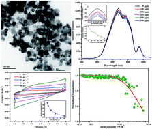
SnO2 nanoparticles (NPs) were prepared by a wet chemical method and characterized by X-ray diffraction (XRD) (rutile tetragonal), Fourier transform infrared spectroscopy (FTIR) (Sn–O, 657 cm−1) and micro Raman spectroscopy (Sn–O, 635 cm−1). From X-ray peak broadening analysis, the crystallite size, lattice strain, deformation stress and energy density values of the tetragonal SnO2 NPs were calculated by modified Williamson–Hall analysis and the size strain plot method. From high resolution transmission electron microscopy (HRTEM), the measured average particle size was determined to be 24 nm. The bandgap was estimated by the Tauc relation as 3.51 eV from UV-visible (UV-vis) spectra. The photoluminescence (PL) spectrum reveals emissions at 382, 416, 440 and 487 nm due to the presence of oxygen defects. Frequency-dependent (42 Hz to 5 MHz) and temperature-dependent (303 to 423 K) electrical properties, such as dielectric constant, loss tangent, AC conductivity and electric modulus, were evaluated by impedance spectroscopy. A SnO2 NPs-clad modified fiber optic gas sensor was used to detect ammonia gas (0 to 500 ppm). The electrochemical performance of the SnO2 NPs electrode has been analyzed by cyclic voltammetry (CV) and galvanostatic charge–discharge (GCD) measurements. Optical limiting measurements for the SnO2 NPs were carried out using a Nd:YAG laser (532 nm, 5 ns, 10 Hz).
1. Introduction
Nanostructured metal oxide semiconductors (MOSs) have received much attention in the past decade due to their size, shape and composition-dependent properties. Compared with other MOSs, SnO2 has excellent electrical, optical and electrochemical properties which have drawn considerable attention for applications as gas sensors, supercapacitors, Li-ion batteries, solar cells, optical wave guides, photocatalysis, etc.1,2
MOS gas sensors can be used for various applications, such as air-quality control, toxic gas detection, and environmental monitoring. Ammonia is a poisonous gas with a pungent smell which is used in refining, cleaning and nitrogenous fertilizers. The Occupational Safety and Health Administration (OSHA) has fixed a limit of 25 ppm in the workplace during an 8 h shift.3 Ishpal Rawal has investigated the ammonia gas sensing properties of SnO2 NPs by the resistivity method (sensitivity: 4.53% at 46 ppm of ammonia at 100 °C).4 Resistive-type sensors are mostly used; however, their sensitivities are poor at room temperature. Recently, fiber optic gas sensors have been fabricated that have greater sensitivity at ambient temperature and are compact and cost effective. The intensity of transmitted light through an optical fiber is very sensitive to optical properties (refractive index, absorption, etc.) which are modulated by gas molecules. Renganathan et al. have demonstrated a nanocrystalline ZnO coated fiber optic sensor for ammonia gas detection.5
Electrochemical capacitors are known as supercapacitors; they deliver high power densities (10 kW kg−1), rapid charge–discharge rates (a few seconds) and longer life cycles (>100
000) than batteries and fuel cells. According to their storage mechanisms, supercapacitors are classified as electric double layer capacitors (EDLCs) and pseudocapacitors; their capacitances are due to charge separation at an electrode/electrolyte interface and reversible faradaic reactions at the electrode surface, respectively.6,7 MOSs (RuO2, Co3O4, NiO and SnO2) have been considered as potential electrode materials in pseudocapacitors due to their high specific capacitances.8 Among these, SnO2 has unique features of high electric conductivity (21.1 Ω cm) and superior electron mobility (100 to 200 cm2 V−1 s−1), which are conducive to energy storage applications. Recently, Venkataramana Bonu et al. have reported the electrochemical supercapacitor performance of SnO2 quantum dots; the observed specific capacitance loss was 9% after increasing the scan rate from 20 to 500 mV s−1.9
Nonlinear optical (NLO) materials play a vital role in photonic applications such as optical switching, optical limiting, optical imaging, memory storage, and quantum communication.10 Among these, optical limiting is significant for protection of the human eye and optical components from high intensity lasers. The visible and near infrared regions (400 to 1400 nm) are considered to be “retinal hazards”, and exposure to these lasers leads to permanent loss of vision in the human eye.11 In recent years, numerous researchers have paid much attention to MOSs to study their optical limiting behaviors due to their remarkable physical and chemical stabilities. Kavitha et al. have shown that pyrrolidone-assisted low temperature-synthesized ZnO nanocones exhibit superior optical limiting behavior.12 Paulose Thomas et al. identified hydrothermally prepared hexagonal shaped nanomorphotype Fe2O3 as a good optical limiter.13
In the present work, a simple wet chemical method has been used to synthesize SnO2 NPs; the NPs have been characterized in detail, including aspects such as microstructural analysis of their size–strain distribution and their morphological, dielectric and linear optical (UV-vis and PL) properties. From an application perspective, the synthesized SnO2 NPs were used to fabricate a fiber optic gas sensor to detect ammonia gas at ambient temperature. Furthermore, the electrochemical performance of the SnO2 NPs was investigated for supercapacitor applications. Finally, the optical limiting behavior of the SnO2 NPs was examined under a pulse regime of 5 ns at a wavelength of 532 nm using a Nd:YAG laser with input energies of 50 and 100 μJ.
2. Experimental section
2.1 Synthesis of SnO2 NPs
3 g tin(II)chloride dihydrate was dissolved in 100 ml double distilled water and stirred for 1 h. 8 M aqueous ammonia was added dropwise to increase the pH to 9, and the solution was stirred at room temperature for 1 h. The white precipitate was maintained undisturbed for 24 h for the nucleation process and centrifuged at 10
000 rpm using double distilled water and ethanol to remove impurities. The powder was dried at 80 °C for 4 h, calcined at 600 °C for 4 h and ground well for further analyses.
2.2 Characterization and measurements
The synthesized SnO2 NPs were characterized by XRD (PANalytical X'Pert Pro, Cu Kα, λ = 1.5406 Å, step size = 0.02° and 2θ range = 10 to 80°). Morphological and compositional analyses were performed by HRTEM (JEOL-JEM-2100F) and EDS (FEI Quanta FEG 200), respectively. Raman spectra (Witec Confocal CDM 200) were recorded with an Ar+ laser (514.5 nm). A Jasco 460 plus FTIR spectrophotometer was used (KBr pellet technique) to confirm the molecular structure. UV-vis (Agilent Cary 60) absorption and fluorescence (Perkin Elmer LS-55) emission spectra were recorded. Dielectric measurements were carried out using a HIOKI (model 3532-50) LCR HiTESTER as a function of frequency (42 Hz to 5 MHz) and temperature (303 to 423 K). The ammonia gas sensitivity was measured using a SnO2 NPs-clad modified fiber optic gas sensor experimental setup as previously reported.5
The electrochemical performance of the SnO2 NPs was examined in a three electrode system (CHI660D electrochemical workstation) using 2 M KOH as the electrolyte. The active material (SnO2), activated carbon and polytetrafluoroethylene were mixed with ethanol with a weight ratio of 85
:
10
:
5. The formed slurry was coated on a graphite sheet (1 cm2) and dried at 80 °C for 8 h. This served as a working electrode. Platinum wire and Ag/AgCl were used as the counter and reference electrodes, respectively.
The third order nonlinear optical properties were investigated by the open aperture Z-scan technique with Q-switched Nd:YAG (Minilite Continum Inc: 532 nm, 5 ns and 10 Hz) laser. The Gaussian beam of the laser pulses was focused by a plano convex lens (focal length: 10.75 cm). The powder sample was dispersed in ethylene glycol (transmittance: 71%), this was added to a 1 mm thick quartz cuvette and placed at the focal point (Z = 0) of the lens on the translation stage. The cuvette was moved stepwise on either side (2.5 cm) of the focal point in the light propagation path (z axis). Two pyroelectric energy detectors were used to monitor the energy of the direct (reference beam) and the transmitted laser beams.
3. Results and discussion
3.1 Structural analysis
Powder XRD of the SnO2 NPs reveals their tetragonal rutile structure (JCPDS no. 41-1445, Fig. 1). The absence of Sn and other impurity peaks indicates the phase purity of SnO2. In order to determine accurate cell parameters of SnO2, Rietveld refinement analysis was carried out using the General Structure Analysis System (GSAS). The refinements of lattice constants, distortion and cell volume are a = b = 4.738 Å, c = 3.181 Å, c/a = 0.671 and V = 71.41 Å3, whereas the fitting parameters Rp (%), Rwp (%) and the χ2 value correspond to 6.3, 7.9 and 0.500, respectively. In order to calculate the crystallite size, lattice strain, stress and energy density values, the following analyses were carried out.
 |
| Fig. 1 XRD pattern of SnO2 NPs by Rietveld refinement. | |
3.1.1 Debye–Scherrer method. Basically, peak broadening in XRD indicates the effects of crystallite size and lattice strain as well as instrumental effects. In order to eliminate the contribution of instrumental broadening, the diffraction pattern of a standard material (silicon) is collected. The corrected instrumental broadening βhkl is used for all the diffraction peaks according to the relation |
βhkl2 = [(βmeasured2) − (βinstrumental2)]1/2
| (1) |
The Debye–Scherrer formula is used to calculate the crystallite size:
|
 | (2) |
where
k is the shape factor (0.94),
λ is the wavelength of the X-ray (1.5406 Å) and
θ is the diffraction angle. To evaluate the crystallite size, lattice strain, stress and energy density, Williamson–Hall (W–H) analysis and the size–strain plot method were used.
14
3.1.2 Williamson–Hall (W–H) analysis.
Uniform density model (UDM). In this model, it is assumed that the crystal is isotropic. Hence, the presence of lattice strain in the material is entirely uniform (all crystallographic directions). Two independent parameters, crystallite size (D) and lattice strain (ε), affect the line broadening. Crystallite size-induced Bragg broadening (βD) is described by rearranging eqn (2), |
 | (3) |
Lattice strain induced broadening (βs) is
|
βs = 4ε tan θ
| (4) |
The combined influence of broadening (βhkl) is given by adding eqn (3) and (4):
|
 | (5) |
By rearranging eqn (5),
|
 | (6) |
The UDM plot (Fig. S1a†) is obtained by plotting βhkl
cos
θ against 4ε
sin
θ. From the graph, the average crystallite size is calculated from the y intercept, and the slope gives the lattice strain.15
Uniform stress deformation model (USDM). In this approach, Williamson–Hall analysis considers the presence of lattice deformation stress which is uniform in all the crystallographic directions. According to Hook's law, the stress (σ) is linearly proportional to the strain (ε) and σ = εE, where E is the Young's modulus or modulus of elasticity in the direction perpendicular to the set of (hkl) planes of the crystal. This law is valid only when very little strain is present in the material. As the strain increases, the particles deviate from this linear proportionality.16 By applying the stress–strain relation in eqn (6), |
 | (7) |
The Young's modulus for all crystallographic directions of a tetragonal crystal system (SnO2) is calculated from the relation17
|
Ehkl−1 = s11(m14 + m24) + s33m34 + (s66 + 2s12)m12m22 + (s44 + 2s13)(m32 + m34)
| (8) |
where
s11,
s12,
s13,
s33,
s44 and
s66 are the six independent elastic compliances (
sij) of SnO
2, and their standard values are 7.43, −4.41, −1.04, 2.95, 9.70 and 4.82 (GPa)
−1, respectively.
18 The graph of
βhkl![[thin space (1/6-em)]](https://www.rsc.org/images/entities/char_2009.gif)
cos
θ vs. 4
![[thin space (1/6-em)]](https://www.rsc.org/images/entities/char_2009.gif)
sin
θ/
Ehkl is shown in Fig. S1b.
† The deformation stress and the crystallite size are extracted from the slope and the intercept on the
y-axis, respectively.
Uniform deformation energy density model (UDEDM). To derive the energy density (u) of the crystal, UDEDM is used. The isotropic and homogeneous nature of the crystal assumed in UDM is not valid for many cases. When the strain energy density ‘u’ is considered, all the constants of proportionality associated with the stress–strain are no longer independent. By Hook's law, the energy density is expressed as u(ε) = ε2Ehkl/2; hence, eqn (6) becomes |
 | (9) |
The plot of βhkl
cos
θ vs. 4
cos
θ(2/Ehkl) gives the UDEDM plot (Fig. S1c†). From the linear fit, the y-intercept yields the crystallite size and the energy density is evaluated from the slope.15
3.1.3 Size strain plot method (SSP). The W–H plot has a positive slope and non-zero intercept; thus, it exhibits the isotropic nature of the crystallites and the presence of microstrain in the SnO2 NPs. However, for better evaluation of the microstructural parameters, the SSP method was adopted, as it gives more importance to low and intermediate angle reflections than higher angles, where the precision is usually lower. Here, it is assumed that the crystallite size and the lattice strain are described by Lorentzian and Gaussian functions, respectively.19 This is of the form |
 | (10) |
where β*f = β*hkl
cos
θ and d* = 1/dhkl. The plot (Fig. S1d†) is drawn between (β*f/d*)2 versus (β*f/d*2). From the graph, the reciprocal of the slope gives the mean apparent size (εβ) of the crystallites. For a spherical shape, the actual crystallite size is estimated using the relation D = 4/3(εβ). The intercept on the y-axis is related to the apparent strain (αβ), and the root mean square strain is calculated from the expression erms = αβ/2(2π)1/2.The geometrical parameters of crystallite size (D), strain (ε), stress (σ) and energy density (u), estimated from various models such as UDM, USDM, UDEDM and SSP, are given in Table 1.
Table 1 Geometric parameters of SnO2 NPs
Debye–Scherrer method |
W–H methods |
Size–strain plot method |
TEM |
UDM |
USDM |
UDEM |
D (nm) |
D (nm) |
ε × 10−3 |
D (nm) |
ε × 10−3 |
σ (MPa) |
D (nm) |
ε × 10−3 |
σ (MPa) |
u (kJ m−3) |
D (nm) |
ε × 10−3 |
σ (MPa) |
u (kJ m−3) |
D (nm) |
16.5 |
22.9 |
1.460 |
19.3 |
0.763 |
200 |
21.1 |
1.247 |
327 |
204 |
27.4 |
1.815 |
476 |
432 |
24 |
3.2 Morphological and elemental analyses
Fig. 2a shows the TEM micrograph of the SnO2 NPs, and their corresponding selected area electron diffraction (SAED) pattern is shown in Fig. 2b. All the diffraction rings in the pattern are in good agreement with the standard data (JCPDS: 41-1445) of tetragonal rutile type SnO2. The particles are spherical, and the size distribution was estimated using Image J software (Fig. 2c); its value is given in Table 1. Fig. 2d and e show HRTEM images of the SnO2 NPs with different magnifications (low and high). From Fig. 2d, a distorted portion of the lattice fringes, indicated by circular rings, clearly exhibits the presence of lattice strain in the prepared SnO2 NPs. This result is consistent with the strain calculated from the X-ray line profile analyses. The calculated d spacing from both of the images (Fig. 2d and e) is 0.331 nm, which corresponds to the (110) plane of SnO2. From the EDS spectrum (Fig. 2f), the presence of Sn and O is confirmed.
 |
| Fig. 2 (a) TEM micrograph, (b) SAED pattern, (c) histogram of particle size distribution, (d) low magnification HRTEM image, (e) high magnification HRTEM image and (f) EDS spectrum of SnO2 NPs. | |
3.3 Raman spectrum
The Raman spectrum (Fig. S2a†) of the SnO2 NPs was recorded at room temperature. In tetragonal SnO2, each unit cell has two tin (Sn) and four oxygen (O) atoms. The six unit cell atoms provide 18 branches for the vibrational modes in the first Brillouin zone. Based on group theory, the normal vibrational modes at the centre of the Brillouin zone are denoted by |
Γ = A1g + A2g + A2u + B1g + B2g + 2B1u + Eg + 3Eu
| (11) |
Among these, B1g, B2g and A1g are non-degenerate modes that vibrate in the plane perpendicular to the c-axis, whereas the doubly degenerated Eg mode vibrates in the direction of the c-axis. Both modes are Raman active. A2u and Eu correspond to the singlet and triply degenerate modes, which are infrared active. A2g and B1u are silent modes. Both Sn and O atoms of vibration along the c-axis correspond to B1u mode, while those vibrations in the plane perpendicular to the c-axis are attributed to Eu mode. From Fig. S2a,† the modes observed at 635 cm−1 (A1g) and 776 cm−1 (B2g) may be related to the expansion and contraction of the vibrating mode of Sn–O bonds, whereas the mode Eg (477 cm−1) is related to the vibration of oxygen in the oxygen plane. The weak peaks at 250, 305, and 346 cm−1 are attributed to the Eu(2) TO, Eu(3) TO and Eu(2) LO modes, respectively. The other peaks at 500, 541 and 691 cm−1 are assigned to the A2u TO, B1u(3) and A2u LO modes, respectively. Among these, the 500 and 691 cm−1 modes were not found in bulk SnO2. Therefore, the appearance of these weak Raman bands for the SnO2 NPs is attributed to the relaxation of the Raman selection rule with increasing surface to volume ratio.20
3.4 FTIR spectrum
The FTIR transmittance spectrum of the SnO2 NPs was recorded by the KBr pellet technique (Fig. S2b†). The prepared SnO2 NPs were calcined at 600 °C for 4 h. The vibrational modes observed at 3440 and 1631 cm−1 (O–H stretching and bending) are due to the water molecules adsorbed by the KBr pellet. Generally, the bands appearing in the lower wavenumber region (430 to 620 cm−1) correspond to the O–Sn–O bridge vibration of SnO2. In the present case, the strong absorption observed at 657 cm−1 is attributed to the characteristic vibration of the Sn–O bond in SnO2.21 The obtained FTIR spectrum was compared with that of bulk SnO2; the positions and shapes of the bands are different.22
3.5 UV-vis absorption spectrum
In the UV-vis spectrum (Fig. S3a†), a peak centered at 284 nm is due to the excitation of the outermost electrons through photon absorption. To calculate the bandgap of SnO2 NPs, the Tauc relation has been used. The expression is given bywhere α is the linear optical absorption coefficient, hv is the photon energy, A is a constant, n = 1/2 for a direct bandgap semiconductor and Eg is the bandgap of the material. An extrapolation of the linear portion of the plot of (αhν)2 vs. hν gives the bandgap value. The calculated bandgap is 3.51 eV, which is red shifted compared to that of bulk SnO2 (3.6 eV).23
3.6 Photoluminescence spectrum
The emission spectrum was recorded at room temperature under an excitation of 275 nm and is shown in Fig. S3b.† The spectrum has several peaks and was resolved by multiple peak fitting. The UV emission at 382 nm (3.25 eV) is lower than the bandgap of SnO2 (3.51 eV), which is not attributed to the direct recombination of a conduction electron in the Sn 4p band and a hole in the O 2p valance band. Instead, the lower emission is attributed to the intrinsic defects (oxygen vacancies, tin interstitials or dangling bonds), which are present in SnO2 NPs.24 In general, oxygen vacancies behave as radiating centres of luminescence in the visible region with different charge states,
, in which
is a very shallow donor. The SnO2 NPs exhibit visible emissions at 416 (2.98 eV), 440 (2.82 eV) and 487 nm (2.54 eV). The origin of these emissions is assigned to the recombination of shallow electrons with the photoexcited holes.23
3.7 Impedance spectroscopy
A SnO2 pellet was subjected to an ac signal, and the frequency–temperature dependent impedance (Z) and phase angle (θ) were measured. From these, the resistive (real Z′) and reactive (imaginary Z′′) components were evaluated using the expressions Z′ = |Z|
cos
θ and Z′′ = |Z|
sin
θ, respectively.25,26 The complex plane of the plot of Z′ versus Z′′ is shown in Fig. 3. In general, it is expected that a succession of three semicircular arcs will emerge in the Cole–Cole plot. Each of these three arcs corresponds to the contribution of the grain interior, the grain boundary and electrode polarization. However, in the present case, a single semicircular arc was observed which is due to the grain interior (bulk) effect alone. The absence of the grain boundary contribution is due to the highly dense nature of the pellet.27 When the temperature was varied (303 to 423 K), the centre of the arc moved towards the origin of the Cole–Cole plot, indicating an activated thermal conduction mechanism.28 The intercept of the circular arc on the X-axis gives the bulk resistance (Rb) of the sample. Using the Rb value, the electrical conductivity was estimated from the following relation: σb = (l/RbA) S cm−1 (l is the thickness and A is the area of the sample). From the Cole–Cole plot, the apex of the arc yields the relaxation frequency (fmax), from which the relaxation time (τb = 1/ωb; ωb = 2πfmax) has been calculated (Table 2).29,30
 |
| Fig. 3 Complex impedance spectra of SnO2 NPs at different temperatures. | |
Table 2 Conductivity parameters of SnO2 NPs
T (K) |
R × 103 (Ω) |
σdc × 10−3 S cm−1 (plots) |
τb (10−5) |
Cb (nF) |
ω × 103 (Hz) |
N × 10−4 (S cm−1 kHz−1) |
μ × 1019 (cm2 V−1 s−1) |
n |
Cole–Cole |
σac |
303 |
41.6 |
1.13 |
1.14 |
5.31 |
1.28 |
19.67 |
0.18 |
40.53 |
0.92 |
323 |
35.6 |
1.33 |
1.43 |
3.98 |
1.12 |
23.05 |
0.20 |
44.55 |
0.91 |
343 |
22.8 |
2.07 |
2.19 |
2.65 |
1.16 |
34.78 |
0.22 |
63.30 |
0.90 |
363 |
13.2 |
3.59 |
3.75 |
1.99 |
1.51 |
49.44 |
0.28 |
85.02 |
0.85 |
383 |
7.7 |
6.15 |
6.18 |
0.79 |
1.03 |
64.41 |
0.37 |
104.97 |
0.80 |
403 |
3.7 |
12.80 |
13.31 |
0.53 |
1.43 |
92.37 |
0.58 |
143.08 |
0.71 |
423 |
1.0 |
47.40 |
48.04 |
0.19 |
1.99 |
185.14 |
1.10 |
273.19 |
0.56 |
Fig. 4a shows Z′ as a function of frequency and temperature. A higher Z′ value is observed in the low frequency region; it decreases with increasing temperature, indicating a gradual enhancement in the ac conductivity. In the higher frequency region, the Z′ values overlap for all the temperatures, which is due to the release of space charge polarization. Z′′ as a function of frequency and temperature is shown in Fig. 4b. The peak of Z′′ decreases with increasing temperature, which also shows the increasing trend of ac conductivity. Noticeable peak broadening is observed from 303 to 423 K, which proves the occurrence of the electrical relaxation process in the material. In addition, there is a shift in the peak to the higher frequency side, which is ascribed to the spread of the relaxation time. The relaxation species of the material involves those electrons at low temperature and oxygen vacancies at higher temperature.31,32
 |
| Fig. 4 Variation of (a) real and (b) imaginary parts of impedance for SnO2 NPs as a function of frequency at different temperatures. | |
3.7.1 Dielectric property. The complex permittivity (ε = ε′ − iε′′) is used to analyze the dielectric properties of materials. The real part (ε′) indicates the stored energy, and the imaginary part (ε′′) denotes the dissipation of energy in the material. The ratio between ε′ and ε′′ gives the loss factor, tan
δ = ε′′/ε′where |
 | (13) |
and |
 | (14) |
here, ω is the angular frequency and C0 is the geometrical capacitance.33 The frequency and temperature dependent ε′, ε′′ and tan
δ of the synthesized SnO2 NPs are shown in Fig. 5a–c. The rotational dielectric polarization (RDP) and surface charge polarization (SCP) are responsible for the dielectric properties of the material. SnO2 is an n-type semiconductor; it possesses a large amount of oxygen vacancies at the interfaces, which play the role of shallow donors. This is evident in the photoluminescence spectrum (Fig. S3b†). The interfaces have a large amount of dipole moments due to the combination of positive oxygen vacancies and negative oxygen ions. When the field is applied, these dipoles rotate and give RDP at the interfaces of the SnO2 NPs. In SCP, the positive and negative space charges located at the interfaces move towards the negative and positive poles of the electric field, respectively. During this motion, the surface charges are trapped by defect sites; finally, dipoles are formed. The SCP contribution is greater in nanomaterials than in their bulk counterparts because of the greater number of interfaces in nanostructured materials (1019/cm3). From Fig. 5a, the value of ε′ increases with increasing temperature at lower frequencies and decreases with increasing frequency. The increase of ε′ with temperature is attributed to the dipoles having free movement at higher temperatures. The decrease of ε′ with increasing frequency occurs because the dipoles are no longer able to rotate because the oscillations lag behind those of the applied field. From Fig. 5b and c, ε′′ and tan
δ show similar behavior to ε′.26,34
 |
| Fig. 5 Frequency dispersion of the (a) real and (b) imaginary parts of the dielectric constant and (c) the dielectric loss of SnO2 NPs. | |
3.7.2 Electrical conductivity. The ac electrical conductivity (σac = ε0ε′′ω) as a function of frequency at a chosen temperature is displayed in Fig. 6.33 The plot contains two distinct portions. A plateau-like region (frequency independent) is seen in the low frequency domain, and the dispersion region (frequency dependent) is seen in the higher frequency domain. The variation of σac obeys the universal Jonscher power law (σac(ω) = σdc + A(ω)n). The first term is the dc conductivity; it is derived from the frequency independent region. The second term is the pure ac conductivity, and it corresponds to the dispersion region, which is a thermally activated quantity. Here, A is the pre-exponential factor, which depends on the temperature and composition of the sample, and n is the frequency exponent term. If n ≤ 1, the hopping motion is associated with translation motion with sudden hopping, whereas for n ≥ 1, the hopping motion suggests localized hopping in which the species does not leave the neighborhood. In our case, the nonlinear curve fitting of the experimental data shows that the entire n values lie between 0 and 1, which implies that the hopping motion involves translation motion. From the dc conductivity, the hopping frequency (ωp), carrier concentration (N) and mobility (μ) are calculated by the following relation, and the obtained values are given in Table 2:35 |
 | (15) |
|
 | (16) |
|
 | (17) |
where e is the charge of the electron.
 |
| Fig. 6 AC conductivity of SnO2 NPs as a function of frequency at different temperatures. | |
3.8 Fiber optic gas sensing applications of SnO2 NPs
Fig. 8a shows the output spectral response of the SnO2 NPs-clad modified fiber optic gas sensor exposed to different concentrations of ammonia (0 to 500 ppm in steps of 100 ppm) at room temperature. The spectral peak around 677 nm decreases continually with increasing gas concentration. The gas sensitivity is defined as the ratio of the change in the peak intensity to the gas concentration. The inset (ii) of Fig. 8a shows the plot of the peak intensity vs. gas concentration. The sensitivity of the sensor was found to be −18 counts for 100 ppm. The negative sign indicates decreasing output intensity with respect to the gas concentration. The absolute value is considered to be the sensitivity. The detailed gas sensing mechanism is reported elsewhere.39 The calculated sensitivity value of the fiber optic gas sensor was compared with other reported work, as given in Table S1.†40–42
 |
| Fig. 8 (a) Fiber optic spectral response of ammonia gas sensor (inset: (i) magnification of 677 nm peak intensity and (ii) plot of peak intensity vs. ammonia gas concentration), (b) CV curves (inset: specific capacitance vs. scan rate), (c) galvanostatic charge–discharge curves (inset: specific capacitance vs. current density) and (d) Ragone plot (inset: cyclic stability (red) and coulombic efficiency (blue)). | |
3.9 Supercapacitor application of SnO2 NPs
Cyclic voltammetry (CV) measurements were made for the SnO2 NPs electrode within the potential range from −1.0 to 0.2 V at different scan rates, as shown in Fig. 8b. The curves depict nearly symmetrical rectangular shapes, indicating good capacitive behavior. The capacitive current density increases with scan rate, demonstrating the good rate capability of the electrode material. The specific capacitance was calculated from the CV curves using the equation |
 | (20) |
Cs is the specific capacitance (F g−1), and Q is the average charge of both the anodic and cathodic scans. m is the mass of the active material, and ΔV is the potential range (V). Based on eqn (20), the estimated Cs values are 334, 282, 213, 163 and 121 F g−1 at the scan rates of 5, 10, 25, 50 and 100 mV s−1, respectively. The inset of Fig. 8b shows the Cs values against the scan rates. The reduction in the capacity at higher scan rates is assigned to the ion exchange mechanism. At lower scan rates, electrolyte ions have sufficient time to intercalate/deintercalate with the interior (active sites) of the electrode material; however, at higher scan rates, the electrolyte ions intercalate/deintercalate mostly at the surface. Fig. 8c shows the almost symmetric triangular shapes of the galvanostatic charge–discharge (GCD) curves of the SnO2 NPs electrode within the potential window of −1.0 to 0.2 V at different current densities. From the GCD curve, the specific capacitance is evaluated using eqn (21), |
 | (21) |
where i is the specific current (A) and Δt is the discharging time (s). The variation of the estimated specific capacitances (1686, 444, 290, 188, 152, 126 and 106 F g−1) against the current densities (2, 5, 10, 20, 30, 40 and 50 mA cm−2) is shown in the inset of Fig. 8c. It can be seen that the specific capacitance decreases as the current density increases. Both CV and GCD evaluation show that the SnO2 electrode is useful in supercapacitor applications. In order to examine the sustainability of the material under continuous cyclic charge/discharge, the electrode was subjected to 400 cycles of charge/discharge at a current density of 50 mA cm−2. The inset (red color) of Fig. 8d shows the calculated Cs values for every fifty cycles up to 400. Even after 400 cycles, there is no capacity degradation. The columbic efficiency was obtained from the relation |
 | (22) |
where td is the discharging time (s), and tc is the charging time (s). The calculated η values at every 50 cycles are shown in the inset (blue color) of Fig. 8d; almost 100% efficiency was achieved. The specific energy density and the power density were determined through the following equations: |
 | (23) |
|
 | (24) |
where E is the energy density (W h kg−1), C is the specific capacitance (F g−1), V is the potential range (V), P is the power density (W kg−1) and t is the discharging time. Fig. 8d depicts the Ragone plot of the SnO2 NPs electrode. The maximum energy density of this material is 337 W h kg−1 at the power density of 600 W kg−1.43,44 The obtained specific capacitance value (1686 F g−1 at mA cm−2) from the GCD measurement was compared with other reported work, which is given in Table S2.†45–48
4. Third order nonlinear optical properties of SnO2 NPs: optical limiting applications
The Z scan technique was employed to investigate the third order nonlinearities, as proposed by Sheik-Bahae et al.49 The intensity-dependent transmittance was measured for the input energies of 50 and 100 μJ. The valley-shaped transmittance curves exhibit the presence of reverse saturable absorption (RSA) in the SnO2 NPs (Fig. 9a and b). Several mechanisms, including nonlinear absorption (NLA) (two or three photon, excited state and free carrier), nonlinear refraction (NLR) and nonlinear scattering are responsible for optical limiting.50 In order to understand the exact nature of the nonlinearity that exists in SnO2, theoretical fitting was performed using the nonlinear transmission equation. The best fit is observed for the two photon absorption along with saturable absorption. The corresponding net nonlinear transmission equation is given by |
 | (25) |
where q(z, 0) = βI0Leff, β is the nonlinear absorption coefficient, I0 is the on-axis peak intensity at the focus (z = 0), Leff = [1 − exp(−αl)]/α is the effective thickness of the sample, α is the linear absorption coefficient, and l is the thickness of the sample cell. When the incident photon energy is higher than the half of the bandgap (hν > Eg/2) of the material, two-photon absorption is possible. In the present scenario, two-photon absorption is allowed, as the input laser energy of 2.33 eV is larger than the halved bandgap of the SnO2 (1.75 eV) NPs. Fig. 10a and b depict the energy dependent optical limiting curves of the sample, which are extracted from the open aperture Z scan experimental data. The input fluence at each z position versus the normalized transmittance of the sample yields the limiting curve. Here, the laser fluence Fin(z) varies with respect to the beam radius ω(z) and the input energy of the laser pulses. Hence, the position dependent fluence for the sample is written as Fin(z) = 4(ln
2)1/2Ein/π3/2ω(z)2, where Ein is the input laser pulse energy and ω(z) = ω(0)[1 + (z/z0)2]1/2, where ω(0) is the beam radius at the focus (15 μm) and z0 (=πω02/λ) is the Rayleigh range.51,52 For low input fluence, the sample transmits light entirely, obeying the Beer–Lambert law; however, for higher input fluence, the sample becomes opaque. In general, optical limiting can occur due to multiphoton absorption (2PA or 3PA) and scattering. In this experiment, a low repetition rate of 10 Hz is used to avoid thermal accumulation in the material, thus ensuring negligible scattering effects. The pulse interval is 0.1 second; within this duration, excited molecules are relaxed to the ground state and the generation of heat will dissipate completely. Hence, thermal buildup in the medium is prevented.53 The onset deviation from the linear transmission as limiting threshold and the estimated values are given in Table 3.54 In addition, the obtained nonlinear parameters have been compared with other NLO materials under the same excitation conditions (Table S3†).52,55–58
 |
| Fig. 9 Open aperture Z scan traces of SnO2 NPs at (a) 50 μJ and (b) 100 μJ. | |
 |
| Fig. 10 Optical limiting curves of SnO2 NPs at (a) 50 μJ and (b) 100 μJ. | |
Table 3 Nonlinear optical parameters (NLO) of SnO2 NPs
Energy (μJ) |
Two-photon absorption coefficient β × 10−11 m W−1 |
Saturation intensity Is × 1011 (W m−2) |
Optical limiting threshold (J cm−2) |
50 |
1.7 |
167.1 |
3.18 |
100 |
2.1 |
120.1 |
2.83 |
5. Conclusion
The crystallite size estimated from modified W–H and SSP methods coincides with that determined by TEM micrography. The presence of lattice strain in the SnO2 NPs was confirmed by HRTEM. The dielectric behavior exhibited by the SnO2 pellet can be exploited for high density energy storage applications. A SnO2 NPs-clad modified fiber optic gas sensor was used to detect ammonia gas at ambient temperature, and its sensitivity was found to be 18 counts/100 ppm. The SnO2 NPs electrode exhibits a maximum specific capacitance of 1686 F g−1 at 2 mA cm−2. This result suggests that it is a suitable electrode material for high performance supercapacitor applications. The nonlinear optical properties of the SnO2 NPs, examined with 532 nm laser pulses, reveals limiting behavior with a threshold value of 2.83 J cm−2. Hence, SnO2 NPs are a potential candidate as an optical limiter to protect optical devices and human eyes from high intensity laser light.
Acknowledgements
One of the authors (K. M.) sincerely acknowledges the Bharathidasan University, Tiruchirappalli, for the award of a University Research Fellowship (Ref. No. 05441/URF/K7/2013). The authors thank the Department of Science and Technology, Government of India for the instrumentation facilities under the DST-FIST program.
References
- R. K. Selvan, I. Perelshtein, N. Perkas and A. Gedanken, J. Phys. Chem. C, 2008, 112, 1825 CAS.
- L. Wang, S. Wang, Y. Wang, H. Zhang, Y. Kang and W. Huang, Sens. Actuators, B, 2013, 188, 85 CrossRef CAS.
- Z. Ye, Y. Jiang, H. Tai, N. Guo, G. Xie and Z. Yuan, J. Mater. Sci.: Mater. Electron., 2015, 26, 833 CrossRef CAS.
- I. Rawal, RSC Adv., 2015, 5, 4135 RSC.
- B. Renganathan, D. Sastikumar, G. Gobi, N. R. Yogamalar and A. C. Bose, Opt. Laser Technol., 2011, 43, 1398 CrossRef CAS.
- F. Zhou, Q. Liu, J. Gu, W. Zhang and D. Zhang, J. Power Sources, 2015, 273, 945 CrossRef CAS.
- Y. Yang, S. Ren, S. Ma, C. Hao and M. Ji, Electrochim. Acta, 2015, 155, 437 CrossRef CAS.
- H. Xia, C. Honga, X. Shia, B. Lia, G. Yuana, Q. Yaoc and J. Xie, J. Mater. Chem. A, 2015, 3, 1216 CAS.
- V. Bonu, B. Gupta, S. Chandra, A. Das, S. Dhara and A. K. Tyagi, Electrochim. Acta, 2016, 203, 230 CrossRef CAS.
- R. Udayabhaskar, M. Shafi Ollakkan and B. Karthikeyan, Appl. Phys. Lett., 2014, 104, 013107 CrossRef.
- S. Dhanuskodi, T. C. Sabari Girisun, N. Smijesh and R. Philip, Chem. Phys. Lett., 2010, 486, 80 CrossRef CAS.
- M. K. Kavitha, H. John and P. Gopinath, Mater. Res. Bull., 2014, 49, 132 CrossRef CAS.
- P. Thomas, P. Sreekanth and K. E. Abraham, J. Appl. Phys., 2015, 117, 053103 CrossRef.
- R. Yogamalar, R. Srinivasan, A. Vinu, K. Ariga and A. C. Bose, Solid State Commun., 2009, 149, 1919 CrossRef CAS.
- A. Khorsand Zak, W. H. A. Majid, M. E. Abrishami and R. Yousefi, Solid State Sci., 2011, 13, 251 CrossRef CAS.
- S. Amreetha and S. Dhanuskodi, Spectrochim. Acta, Part A, 2014, 127, 543 CrossRef PubMed.
- J. F. Nye, Physical Properties of Crystals: Their Representation by Tensors and Matrices, Oxford, New York, 1985 Search PubMed.
- V. Consonni, G. Rey, H. Roussel and D. Bellet, J. Appl. Phys., 2012, 111, 033523 CrossRef.
- M. A. Tagliente and M. Massaro, Nucl. Instrum. Methods Phys. Res., Sect. B, 2008, 266, 1055 CrossRef CAS.
- K. C. Verma and R. K. Kotnala, Phys. Chem. Chem. Phys., 2016, 18, 17565 RSC.
- J. Kaur, J. Shah, R. K. Kotnala and K. C. Verma, Ceram. Int., 2012, 38, 5563 CrossRef CAS.
- S. Emiroglu, N. Barsan, U. Weimar and V. Hoffmann, Thin Solid Films, 2001, 391, 176 CrossRef CAS.
- A. S. Ahmed, S. M. Muhamed, M. L. Singla, S. Tabassum, A. H. Naqvi and A. Azam, J. Lumin., 2011, 131, 1 CrossRef CAS.
- K. Srinivas, M. Vithal, B. Sreedhar, M. M. Raja and P. V. Reddy, J. Phys. Chem. C, 2009, 113, 3543 CAS.
- N. Panda, B. N. Parida, R. Padhee and R. N. P. Choudhary, J. Mater. Sci.: Mater. Electron., 2015, 26, 3797 CrossRef CAS.
- N. Kumari, A. Ghosh and A. Bhattacharjee, Mater. Sci. Semicond. Process., 2014, 19, 114 CrossRef CAS.
- A. Nandy, C. S. Tiwary, A. Dutta, K. Chattopadhyay and S. K. Pradhan, Electrochim. Acta, 2015, 170, 360 CrossRef CAS.
- W. B. Soltan, M. Mbarki, S. Ammar, O. Babot and T. Toupance, J. Mater. Sci.: Mater. Electron., 2015, 26, 1612 CrossRef.
- A. Azam, A. S. Ahmed, M. Chaman and A. H. Naqvi, J. Appl. Phys., 2010, 108, 094329 CrossRef.
- S. Lanfredi and A. C. M. Rodrigues, J. Appl. Phys., 1999, 86, 2215 CrossRef CAS.
- R. Bargougui, A. Oueslati, G. Schmerber, C. Ulhaq-Bouillet, S. Colis, F. Hlel, S. Ammar and A. Dinia, J. Mater. Sci.: Mater. Electron., 2014, 25, 2066 CrossRef CAS.
- S. Sen, R. N. P. Choudhary, A. Tarafdar and P. Pramanik, J. Appl. Phys., 2006, 99, 124114 CrossRef.
- H. M. Chenari, A. Hassanzadeh, M. M. Golzan, H. Sedghi and M. Talebian, Curr. Appl. Phys, 2011, 11, 409 CrossRef.
- A. S. Lanje, S. J. Sharma, R. S. Ningthoujam, J. S. Ahn and R. B. Pode, Adv. Powder Technol., 2013, 24, 331 CrossRef CAS.
- V. D. Nithya and R. K. Selvan, Phys. B, 2011, 406, 24 CrossRef CAS.
- J. Zhang, M. Mine, D. Zhu and M. Matsuo, Carbon, 2009, 47, 1311 CrossRef CAS.
- A. S. A. Khiar, R. Puteh and A. K. Arof, Phys. B, 2006, 373, 23 CrossRef CAS.
- B. Behera, P. Nayak and R. N. P. Choudhary, J. Alloys Compd., 2007, 436, 226 CrossRef CAS.
- R. Mohandoss, S. Dhanuskodi, B. Renganathan and D. Sastikumar, Sens. Actuators, A, 2013, 203, 310 CrossRef CAS.
- L. R. Shobin, B. Renganathan, D. Sastikumar, K. C. Park and S. Manivannan, IEEE Sens. J., 2014, 14, 1238 CrossRef CAS.
- B. Renganathan, D. Sastikumar, G. Gobi, N. R. Yogamalar and A. Chandra Bose, Sens. Actuators, A, 2011, 156, 263 CrossRef CAS.
- L. R. Shobin, D. Sastikumar and S. Manivannan, Sens. Actuators, A, 2014, 214, 74 CrossRef CAS.
- M. Chen, H. Wang, L. Li, Z. Zhang, C. Wang, Y. Liu, W. Wang and J. Gao, ACS Appl. Mater. Interfaces., 2014, 6, 14327 CAS.
- S. Nagamuthu, S. Vijayakumar and G. Muralidharan, Dalton Trans., 2014, 43, 17528 RSC.
- S. E. Moosavifard, M. F. El-Kady, M. S. Rahmanifar, R. B. Kaner and M. F. Mousavi, ACS Appl. Mater. Interfaces, 2015, 7, 4851 CAS.
- N. Duraisamy, A. Numan, S. O. Fatin, K. Ramesh and S. Ramesh, J. Colloid Interface Sci., 2016, 471, 136 CrossRef CAS PubMed.
- X. Wang, X. Wu, B. Xu and T. Hua, J. Solid State Electrochem., 2016, 20, 1303 CrossRef CAS.
- M. Lu, Y. Lu, K. Qiu, J. Cheng, H. Yan and Y. Luo, Mater. Lett., 2016, 166, 255 CrossRef CAS.
- M. S. Bahae, A. A. Said, T. H. Wei, D. J. Hagan and E. W. Vanstryland, IEEE J. Quantum Electron., 1990, 26, 760 CrossRef.
- Z. Chann, L. Wei, C. Wenzhe, Y. Xiaoyun, C. Shuguang and X. Xueqing, Ceram. Int., 2014, 40, 2669 CrossRef.
- M. K. Kavitha, H. John, P. Gopinath and R. Philip, J. Mater. Chem. C, 2013, 1, 3669 RSC.
- B. Karthikeyan, R. Udayabhaskar, T. Priya Rose, T. Pandiyarajan and R. Philip, RSC Adv., 2014, 4, 39541 RSC.
- B. Anand, A. Kaniyoor, D. Swain, T. T. Baby, S. V. Rao, S. S. S. Sai, S. Ramaprabhu and R. Philip, J. Mater. Chem. C, 2014, 2, 10116 RSC.
- M. N. Muralidharan, S. Mathew, A. Seema, P. Radhakrishnan and T. Kurian, Mater. Chem. Phys., 2016, 171, 367 CrossRef CAS.
- J. J. Wu, Y. R. Tao, J. N. Wang, Z. Y. Wu, L. Fan and X. C. Wu, Nanoscale, 2016, 8, 10371 RSC.
- R. P. Ummer, P. Sreekanth, B. Raneesh, R. Philip, D. Rouxel, S. Thomas and K. Nandakumar, RSC Adv., 2015, 5, 67157 RSC.
- B. S. Kalanoor, L. Gouda, R. Gottesman, S. Tirosh, E. Haltzi, A. Zaban and Y. R. Tischler, ACS Photonics, 2016, 3, 361 CrossRef CAS.
- B. Raneesh, K. Nandakumar, A. Saha, D. Das, H. Soumya, J. Philip, P. Sreekanth and R. Philip, RSC Adv., 2015, 5, 12480 RSC.
Footnote |
† Electronic supplementary information (ESI) available. See DOI: 10.1039/c6ra20503h |
|
This journal is © The Royal Society of Chemistry 2016 |
Click here to see how this site uses Cookies. View our privacy policy here.