Spark plasma sintering route to synthesize aluminium doped zinc oxide

Sonia Sharma, Raghavendar Bayikadi and P. Swaminathan*
Department of Metallurgical and Materials Engineering, IIT Madras, Chennai-600036, India. E-mail: swamnthn@iitm.ac.in

Received 12th August 2016 , Accepted 5th September 2016

First published on 5th September 2016


Abstract

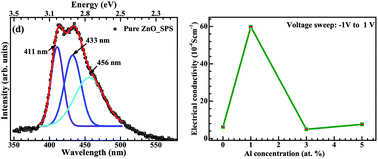
Aluminium doped zinc oxide is prepared using spark plasma sintering. The process leads to a tailored optical band gap extending into the visible region with increasing aluminium concentration. Microstructural, optical, and electrical characterization were carried out to investigate the effect of the sintering process and aluminium concentration on the grain size, band gap, and electrical conductivity. The delocalization of impurity energy states created during sintering, causes band gap narrowing and leads to an improved conductivity. The impurity states are primarily oxygen vacancies and zinc interstitials. Spark plasma sintering offers a promising approach to synthesize doped conductive metal oxides with control over the band gap and can be extended to a variety of other systems.


Introduction

There is an increased use of electronic devices and a concomitant rise in power consumption. In order to meet the expectations of the next generation devices, the search for alternative energy sources has increased around the world. Solar cells are easily manufactured, efficient devices for harnessing energy.1 They operate on the principle of an active absorber, which converts the incident energy into charge carriers. These carriers are then separated and extracted to the external circuit using suitable electrodes. There are a wide variety of absorbers, but common to all solar cells is the requirement of optically transparent and electrically conductive electrodes, especially in the direction of light absorption. Indium doped tin oxide (ITO) has been the material of choice,2–4 but the high cost of indium has forced the search for alternates. Zinc oxide (ZnO) is one such candidate for a transparent conducting electrode replacing ITO. Pure ZnO has a wide direct band gap of 3.3 eV, which lies in the UV region.5 It is an n-type, non-degenerate semiconductor, but has a higher electrical resistivity than ITO.6 For transparent conducting applications, the resistivity has to be lowered, and this is achieved by doping with suitable elements.2 Doping causes shift in the optical band gap, which is defined as the energy corresponding to the sharp increase in light absorption.6 The processing route also determines the band gap of the material, with defects states affecting both conductivity and transparency.5,7,8

Pure ZnO has a wurtzite type hexagonal structure possessing anisotropic properties along the c-axis.6 It has many applications, ranging from photovoltaic electrodes, piezoelectric transducers, flat panel displays, solar cell windows, UV light emitters, and bulk acoustic wave devices.1,2,6,9 It is possible to modify the physical, chemical, electrical, and optical properties of ZnO by doping with suitable elements.10 Recently, we showed that Mn doping in ZnO shifts the optical band gap closer to the red end of the spectrum. We attributed this shift to the formation of defect states due to Mn substitution in the Zn sites and the variable valency exhibited by Mn.11 Electrical properties are also influenced if doping is carried out using a higher valence atom at the Zn site.12 The difference in valency can lead to an increase in charge carriers, which can cause an increase in conductivity. Doping in ZnO has been achieved using wet chemical methods, such as sol gel and co-precipitation methods,7 and physical synthesis methods, such as pulsed laser deposition, thermal evaporation, sputtering, and solid state synthesis.13–15 It is also possible to increase carrier concentration in pure ZnO, by processing under reducing conditions (high vacuum or hydrogen atmosphere).16,17 Among the large number of dopant materials available, Al doped ZnO (AZO) is a prime candidate for transparent conductor applications.9

In this paper, we used spark plasma sintering (SPS), which is a solid state synthesis technique, for preparing AZO. SPS is an electric current assisted sintering process, where a localized plasma is created between the particles by application of a direct current pulse.18 The advantages of SPS include fast heating and cooling rates, short holding time, and the possibility of applying loads during sintering. The short holding time limits phase segregation and helps in obtaining a highly dense material.19,20 The process is carried out in a high vacuum chamber, which can generate defect structures, with modified optical and electrical properties. In AZO, the amount of Al doping possible can be determined using the phase diagram, which describes the maximum solubility of Al in ZnO.21 The phase diagram shows a room temperature solid solubility of Al in ZnO up to 2 at% and formation of a two phase region beyond 2 at%. In this work, AZO samples with formula AlxZn1−xO, with x from 0 to 0.05, were synthesized using SPS. The phases obtained were characterized by X-ray diffraction (XRD), scanning electron microscopy (SEM) with energy dispersive spectroscopy (EDS), Raman spectroscopy, and X-ray photoelectron spectroscopy (XPS). Optical properties were measured using diffuse reflectance spectroscopy (DRS), and the optical band gap was extracted from the data. We show that the shift in optical band gap towards the visible region depends on the generation of oxygen vacancies and zinc interstitials during the SPS process. Doping also plays a role in this shift, as seen by comparing pure ZnO and AZO subject to SPS under the same conditions. Electrical conductivity data shows an increase with respect to pure ZnO, up to a certain dopant concentration, followed by a decrease. The increase was attributed to the introduction of an extra electron for each Zn atom replaced by Al (due to the change in valency from +2 to +3), while the increased scattering due to higher defect concentration and formation of a secondary phase is responsible for the lowering of the conductivity with increased doping.

Experimental details

High purity zinc oxide and alumina powders were sourced from Sigma-Aldrich. We prepared powders with composition AlxZn1−xO, (where, x = 0, 0.01, 0.03, 0.05) by mixing the powders in the appropriate molar ratio. Before SPS, ball milling was carried out using zirconia balls of diameter 3–8 mm, keeping the ball to powder ratio 20[thin space (1/6-em)]:[thin space (1/6-em)]1. The milling was carried out in toluene media for 12 h to reduce the particle size to the nanometre level. This increases the reactivity of the constituents and consequently lowers the SPS temperature. After ball milling, the powder was dried overnight at room temperature to remove excess toluene and the mixture was loaded into a graphite mould inside the vacuum chamber of the SPS system (DR. SINTER system from SPS Syntax Inc., Japan). Graphite die and punch of diameter 10 mm were used for holding the sample in the chamber. Powders were sintered in vacuum (<10−5 Pa) at 1100 °C while a 50 MPa load was applied. The holding time was fixed at 5 min and the sample heating rate was set to 100 °C min−1. The sintered pellets were approximately 10 mm in diameter and 4 mm in thickness.

After SPS, the pellets were characterized using a Bruker D8 X-ray diffractometer with Cu Kα (λ = 0.154 nm) radiation (20° ≤ 2θ ≤ 90°). SEM with EDS attachment was used for analysing the morphology and composition. The EDS data was obtained from Quanta 200, which uses a thermionic tungsten filament, while high resolution imaging was carried out in an FEI Inspect F SEM, which uses a field emission gun. Raman scattering experiments were performed using a WiTec spectrophotometer in the wave number range 10–1200 cm−1. A polarized light He–Ne laser, with wavelength of 532 nm, was used and the scattered light was detected by a charge coupled device based detector. Photoluminescence (PL) spectra was obtained from Horiba Jobin-Yvon PL spectrometer and DRS was recorded in an Ocean optics UV2000 UV-Vis spectrophotometer. Chemical binding states were characterized by XPS measurements on a K-alpha Thermos scientific. Electrical conductivity of the sintered pellets was measured using a Summit 11000M probe station from Cascade Micro Tech, in the four point probe configuration.

Results and discussion

Structural analysis and surface morphology study

XRD patterns of the SPS sintered samples, seen in Fig. 1(a), show sharp peaks indicating high crystallinity and long range structural order. These patterns can be matched with pure ZnO, ICSD file 98-002-8860. A portion of the XRD data, containing the three highest intensity peaks, is focused in Fig. 1(b). The peak positions for pure and doped (Al0.01Zn0.99O) pellets, both subjected to SPS under the same conditions, are shifted towards a lower angle with respect to the standard ICSD pattern. This shift can be attributed to the formation of defects during SPS, notably zinc interstitials (Zni), which cause an increase in the lattice parameter and hence a shift towards lower angles.3 In 1% and 3% AZO no secondary phase is observed in the XRD pattern. Thus, within the detection limits of XRD, we conclude the presence of a single phase, with the incorporation of the Al dopants into the lattice sites in the host ZnO. The ionic radius of Zn2+ (0.072 nm) is larger than that of Al3+ (0.054 nm)22 and therefore Al substitution should decrease the lattice parameter and shift the peaks towards larger Bragg angles. The opposite effect is seen for the 1% AZO case in Fig. 1(b). This is because the defects created during SPS are responsible for the peak shift, overwhelming the difference in ionic radii. However, on increasing the Al concentration, the peak shifts towards higher angles with respect to pure ZnO produced by SPS, as seen in Fig. 2. The figure also shows that with increasing Al concentration there is a secondary phase, indexed to ZnAl2O4, ICSD file 98-006-6200, for 5% doped AZO. This is consistent with the phase diagram, which predicts the formation of gahnite mineral, above 2 mol% of Al2O3 in ZnO.21
image file: c6ra20396e-f1.tif
Fig. 1 (a) X-ray diffraction patterns for pure ZnO and Al0.01Zn0.99O after spark plasma sintering at 1100 °C for 5 min. The patterns can be matched with pure ZnO, with no secondary phases formed. (b) Comparison of the three prominent ZnO peaks showing a peak shift towards lower angle with respect to the standard pattern. The shift is marked on the (011) peak by thin dotted lines. Both samples were processed and annealed under the same conditions.

image file: c6ra20396e-f2.tif
Fig. 2 (a) X-ray diffraction patterns for AlxZn1−xO; (0.01 ≤ x ≤ 0.05) after spark plasma sintering at 1100 °C for 5 min. A single phase is seen for 1% and 3% AZO, while 5% AZO shows the presence of a secondary phase, ZnAl2O4. (b) Comparison of the three prominent ZnO peaks of Al doped ZnO showing a peak shift towards right with respect to 1 at% Al doped ZnO. The shift confirms the substitution of the smaller Al ion at the Zn site.

Another reason for peak shift could be stresses in the material during processing. Ball milling introduces compressive stresses in the powder3,23 and the applied load in SPS is also compressive in nature. These stresses can lower the lattice spacing and shift the XRD peaks to higher angles. This is again opposite to the shift observed in Fig. 1 and 2, especially when comparing pure ZnO as received and after SPS. Hence, stresses can be ruled out as the cause for the peak shift. SPS processing can also cause anisotropic grain growth, especially for grains near the surface. The XRD plot in Fig. 1 shows higher intensity along (002) and (013) for the SPS samples compared to the standard powder pattern. One way to explain this discrepancy is by attributing the intensity difference to the presence of a second phase such as ZnAl2O4, or any unreacted Al2O3. But this secondary phase is not seen until we have 5% Al. Hence, we hypothesize that this intensity difference is due to anisotropic grain growth in the SPS process, primarily in grains within few microns depth from the surface. Similar anisotropic grain growth has been seen for other materials processed by SPS.24 To check our assertion, XRD was recorded for the SPS samples, both in the pellet form and after crushing it into powder. Since the penetration depth of X-rays is of the order of a few microns, in pellet form the layers closest to the surface are involved in diffraction, while in powder form the diffraction is from a mixed region. If the peaks were due to a secondary phase, then the relative intensities should be the same for both cases. But, comparing the XRD peaks shows that for the crushed powder the relative intensities are similar to the standard ICSD pattern. This implies that the increase in intensity is due to the anisotropy generated during SPS and not due to the formation of a secondary phase.24,25 These oriented grains are located closer to the surface than the bulk and are likely formed due to the fast cooling rate at the surface compared to the bulk. XRD patterns in Fig. 2 revealed that the peak positions continuously changed with increasing doping. Also, the peaks are symmetric and show decreased broadening when the pellets are crushed into powder form. The reason for broadening in SPS sample can be attributed to presence of fine grains at and near the surface with larger grains nearer to the centre.

The morphology, distribution, and elemental composition of the sintered materials were investigated using SEM and EDS. Fig. 3(a and b) shows SEM images of 5 at% AZO SPS pellets crushed into powder. These figures are representative images of the samples at two different magnifications. The typical particle size is less than 500 nm with a broad inhomogeneous distribution of sizes. This can be due to difference in size of the grains at the surface and the core of the pellet. Fig. 3(c and d) shows the grains present in a cross section of the pellet. Surface grains are fine with sizes of the order of 50 nm but becomes larger with increasing depth (sizes of the order of 1 μm). This microstructural gradient likely results from the thermal gradient in the pellet. The low thermal conductivity of the material, fast heating and cooling times, and short holding times prevent temperature equilibration causing this size distribution.26 Fig. 4 compares the grain size for pure ZnO and 1 at% AZO. Al incorporation gives finer grains because the added alumina suppresses grain boundary mobility and reduces the grain growth.20 EDS data is used to estimate the amount of Al in AlxZn1−xO samples. This data is collected from the crushed pellets and tabulated in Table 1. The average concentration of Al is qualitatively comparable to the doped value, with possible local variations in individual grains.


image file: c6ra20396e-f3.tif
Fig. 3 (a and b) shows scanning electron micrographs of 5 at% AZO SPS powder sample. These figures are representative images at increasing magnifications. Typical particle size is less than 500 nm. (c and d) shows the fine grains present at and below the surface of sintered pure ZnO sample.

image file: c6ra20396e-f4.tif
Fig. 4 Image quality map obtained from SEM for (a) pure ZnO (b) 1 at% AZO after SPS. The grain size is finer for doped ZnO because the presence of Al prevents grain growth.
Table 1 EDS data of AlxZn1−xO (0.01 ≤ x ≤ 0.05) shows the relative percentages of Zn and Al for the three different AZO samples. The values obtained from EDS agree qualitatively with the intended dopant concentration
Sample name Element At%
1% AZO Al 01.90
Zn 70.32
3% AZO Al 04.38
Zn 33.53
5% AZO Al 04.94
Zn 45.57


Defect formation in SPS processing

To understand the effect of milling and SPS on the creation of structural defects such as zinc interstitials (Zni) and oxygen vacancies (VO), micro-Raman spectroscopy was used. Since the formation of defects affects the optical and electrical properties, understanding their origin is crucial. ZnO belongs to the C6V symmetry group, which has two A1, two E1, two E2, and two B1 modes.27 Among these, A1 and E1 modes are polar and are further split into transverse optical (TO) and longitudinal optical (LO) phonons, all being Raman and infrared active. E2 modes are only Raman active and B1 modes are infrared and Raman inactive (silent modes). The A1 modes are related to intrinsic defects such as VO and Zni.16,28 Fig. 5(a) shows the Raman spectra for pure ZnO samples in three stages: as received, after ball milling, and after SPS. There is minimal change in the spectra after ball milling, but post-SPS, the peaks shift to lower wave numbers. The possible reasons for this shift could be point defects, lattice strain, and/or phonon confinement.16 Fig. 5(b), compares the Raman spectra for the three AZO samples. The spectra look similar to each other and also to the pure ZnO post-SPS, indicating that the defect creation is influenced by SPS rather than doping.
image file: c6ra20396e-f5.tif
Fig. 5 (a) Room temperature Raman spectra of pure ZnO as received, 12 h ball milled, and after SPS. The process gives rise to a peak shift to the left with respect to pure ZnO powder. (b) Comparison of the Raman spectra for the three doped AZO samples. The spectra are similar indicating that the SPS process is mainly responsible for defect creation.

Consider the A1 (LO) peak at 576.7 cm−1, marked in Fig. 5(a), associated with the intrinsic lattice defects. Since ball milling is carried out in a toluene medium, the oxygen vacancy concentration (VO) remains stable. However, when these samples were sintered at 1100 °C in the SPS, in an oxygen deficient environment, oxygen vacancies and interstitial zinc can form and this causes a shift towards a lower wave number (red shift). The peaks at 384 and 411 cm−1 are related to the A1 (TO) and E1 (TO) modes of ZnO, which reflect the strength of polar lattice bond. The A1 (TO) peak at 384 cm−1 is suppressed by SPS while the E2 (high) − E2 (low) and A1 (LO) are increased after SPS, compared to the as received and ball milled ZnO. This effect is generally attributed to an increase in plasmon–phonon coupling due to increased electron concentration. The polar character of the wurtzite structure is also reduced when defects are formed and when Al3+ ions are incorporated.29,30

The characteristic Raman peak for as received pure ZnO appears at 438 cm−1 (E2 (high)).27 In SPS synthesized ZnO sample, this peak becomes broader and is red shifted towards the lower wavenumber value of 425.9 cm−1. This indicates a change in the band structure of the lattice due to non-stoichiometry, stresses, local heating, and/or size effect of the material. It has been suggested that the mixing of two different cations via doping changes the charge distribution, affecting the local polarizability and can result in at least one vibrational mode being strongly reduced.31 It is observed in all AZO samples that the E2 (high) peak shifts to lower wavenumber and the amount of shift depends on the doping concentration. The E2 (high) peak positions are 425.9 cm−1 (x = 0, 0.01), 432 cm−1 (x = 0.03), and 435.7 cm−1 (x = 0.05) indicating a downward shift of approximately 13.9, 7.9, and 3.1 cm−1 respectively. The red shift in pure ZnO can be attributed to the SPS process because of large local heating and defects generated, resulting in phonon localization.25,29 The activation of second order silent Raman mode (2B1) at 514 cm−1 is attributed to interstitial Zn and O vacancies formed during SPS.32 These defects might be the reason for breakdown of the translational symmetry of the lattice. Al3+ substitution at Zn2+ site may cause decrease in bond length as Al3+ ion has smaller ionic radius thus causing compression and an increase in phonon frequency, which is clearly observed in Al doped ZnO, as shown in Fig. 5(b).33

Defect formation in SPS and influence on optical properties

The PL spectra of as received ZnO (purity > 99.8%), plotted in Fig. 6(a), shows spectrum with near band emission (NBE) at 385 nm and a broad defect region increasing above 600 nm. After ball milling for 12 h, there is no change in the PL spectrum though a small decrease in intensity is seen. This indicates local scattering due to defects created during milling. A similar behaviour was observed for cold compacted pellets of Al2O3–ZnO (before SPS). PL measurements on the SPS samples, Fig. 6(a) and (b), showed a marked difference from the as received and sintered samples. The near-band-edge (NBE) emission peak at 380 nm (3.26 eV) was suppressed in the pure and doped samples post SPS. All samples showed a strong and broad emission band in the violet (400 nm) and blue regions (500 nm), expanded in Fig. 6(c), corresponding to newly created defect centres. These defects, which become active in the visible region, arise due to SPS process parameters, primarily the high temperature and the oxygen-deficient nature of the process. Literature reports show high concentration of zinc interstitials and oxygen vacancies in vacuum treated samples.8,33 Theses defects together can form multiple defect-related levels in the band gap. The gap between the conduction band and the energy level corresponding to oxygen vacancies is considered to be 2.28 eV and that from the interstitial zinc level to the valence band is 2.9 eV.28 To understand the evolution of the broad emission band, it was deconvoluted into three sharp Gaussian peaks with maxima centred at 411 nm (3.02 eV), 433 nm (2.86 eV), and 456 nm (2.7 eV), respectively as shown in Fig. 6(d). It has been reported that the peaks around 411 and 433 nm are related to the direct excitation of the impurities/defect-related levels in the pure and doped samples.34 The violet luminescence at 411 nm has been attributed to the surface zinc vacancy,16 while the blue emission band centred at 433 nm is caused by the transition of excited electrons from the energy level of Zni to the valence band28 or it may originate from the relaxation of electrons excited via the 3d-sp interband transition of interstitial Zn atoms.35 The green-yellow emission centred at 456 nm (2.7 eV) originates from deep level defect emission associated with oxygen vacancies in the lattice. It can also be due to the transition between the shallow donor levels of Zni to the top of the valence band or the transition between shallow acceptor levels of oxygen vacancies and shallow donor levels of the zinc vacancy.12,16,36,37 It has also been reported that the peak at 2.7 eV can be due to the relaxation of electrons in sp–sp interband transition of interstitial Zn metal atom.35 Since these peaks are seen in both pure ZnO and AZO, doping does not play a role in these defect states. Rather it is the nature of the SPS process which creates these defects and modifies the emission properties.
image file: c6ra20396e-f6.tif
Fig. 6 (a) Photoluminescence spectra of pure ZnO as received, 12 h ball milled, and SPS sample. The near band edge emission peak disappeared completely after SPS, while a new defect related emission can be seen. (b) Comparison spectra for the doped samples show that it is same as that of the pure ZnO sample. (c) The defects states for the three doped samples are shown. (d) Fitted spectra of pure ZnO pellet shows that the broad peak can be deconvoluted into three peaks fitting in the range from 380–520 nm.

As received ZnO powder is white in color due to scattering of light from the individual particles. After ball milling for 12 hours, the color changed to pale yellow indicating a red shift in the absorption edge. Post-SPS, the absorption edge is shifted further towards longer wavelengths as shown in Fig. 7(a). The optical band gap values for SPS processed ZnO and AZO were calculated from the reflectance spectra using the standard Kubelka-Munk function5 and listed in Table 2. There is not much variation between the AZO samples and this provides a strong indication that the Zn ions are only partly substituted by the Al ions and with increasing Al concentration a secondary phase is formed rather than doping into the matrix. This is also consistent with the phase diagram which shows limited solid solubility.


image file: c6ra20396e-f7.tif
Fig. 7 (a) Plots of the Kubelka-Munk function vs. photon energy for pure ZnO as received, 12 h ball milled, and after SPS. A red shift is observed because of ball milling and sintering. (b) The doped ZnO spectra are red-shifted with respect to the pure samples. The x-intercept of the slope was used to calculate the band gap and the values are listed in Table 2.
Table 2 Optical band gap values calculated from plots of Kubelka-Munk function vs. photon energy, shown in Fig. 7. The band gaps are obtained by taking the x-intercept of the straight line fit to the slope. For pure ZnO, ball milled, and SPS samples band gap decreases compared to the as received sample. AZO shows further band gap narrowing and it is relatively independent of the doping concentration
AlxZn1−xO, values of x Band gap (eV)
0 Pure ZnO 3.19 ± 0.89
Pure ZnO ball milled 3.07 ± 0.86
ZnO post SPS 2.82 ± 0.43
0.01 1% AZO 2.62 ± 0.26
0.03 3% AZO 2.73 ± 0.29
0.05 5% AZO 2.78 ± 0.31


The lowering of the optical band gap can be explained by the formation of defects during SPS. Oxygen vacancies are generated during the processing in the vacuum environment. The higher ionic radius of oxygen (O2− = 126 nm) compared to the zinc ion (Zn2+ = 88 nm) means that there is a low possibility of the oxygen atom going into the interstitial position.19 When alumina is added oxygen vacancies decrease on incorporation of Al into ZnO, as predicted in eqn (1).38,39

 
image file: c6ra20396e-t1.tif(1)

The incorporation of Al in the ZnO lattice causes the oxygen to occupy interstitial position. The Zn atom that is displaced from its lattice site forms an interstitial. When the concentration of Zn interstitials increase there is a possibility for impurity states to become delocalized and overlap with the conduction band edge, effectively lowering the optical band gap of the material. In case of AZO, along with the defects, doping also introduces shallow-donor impurities40 and these impurities create energy levels in the band gap near the conduction band edge. With increase in the amount of doping, the density of states of these dopants increase and this forms an impurity band overlapping with the ZnO energy bands and effectively reducing the band gap. This explains the further drop in optical band gap for AZO compared to pure ZnO subjected to SPS.

Chemical bonding state and component analysis

X-ray photoelectron spectroscopy is a useful tool to analyse the valence states of the constituents in a material. Fig. 8 shows a XPS scan of pure ZnO after SPS. The binding energy of C 1s, at 284.6 eV, was used as an internal reference to calibrate the peaks. Slow scans were also performed around the O 1s, Zn 2p, and Zn LMM peaks to obtain further information on the chemical state of the elements.9 The oxygen 1s spectrum is shown in Fig. 9(a) and can be fitted with two peaks, one at 530.42 ± 0.01 eV and the other at 531.74 ± 0.03 eV. The first peak corresponds to the oxygen atoms in a fully-coordinated environment with the metal ions in the wurtzite structure of ZnO and the second peak to the oxide ion in oxygen-deficient regions. In the case of 3% AZO, the first peak was at 529.88 ± 0.03 eV and the second peak at 531.48 ± 0.01 eV as obtained from Gaussian fits to the data and shown in Fig. 9(b). The main difference between pure ZnO and AZO is the relative intensity of the two peaks, with the higher energy peak dominating in AZO. Since this peak represents oxygen in a defect environment we can conclude that the Al doping leads to the preferential generation of certain types of defects in AZO.25
image file: c6ra20396e-f8.tif
Fig. 8 Full scan XPS spectrum of pure ZnO sample using SPS. Zn, O, and C peaks are seen. The C 1s peak was used as an internal standard to calibrate the peak positions.

image file: c6ra20396e-f9.tif
Fig. 9 XPS spectra O 1s of the ZnO SPS samples sintered at 1100 °C. (a) Pure ZnO, (b) Al0.03Zn0.97O. The 1s spectra can be fitted by two Gaussian peaks. The first one corresponds to the oxygen peak in its lattice site while the second one corresponds to O in a defect site.

The Zn 2p spectrum shows a doublet whose binding energies are 1023.03 eV and 1045.58 eV which can be assigned to Zn 2p3/2 and Zn 2p1/2 lines, respectively. The binding energy difference between the two lines is 23.10 eV, which corresponds well with the standard reference value for ZnO.41 The binding energy and the binding energy difference value calculated from our XPS spectrum show that Zn atoms are in +2 oxidation state. The Zn 2p3/2 peak shown in Fig. 10(a), is asymmetric and can be deconvoluted into two components, a peak at 1021.58 ± 0.02 eV assigned to metallic zinc with zero valency (this corresponds to Zn interstitial defects in the matrix) and a peak at 1023.38 ± 0.12 eV assigned to Zn–O bond in the crystal.5,35 To further confirm the presence of zinc interstitials we looked at the Zn LMM Auger peak, plotted in Fig. 10(c) and (d). This peak can also be deconvoluted into two, centred at 496.93 ± 0.16 eV and 499.42 ± 0.12 eV. These can be assigned to interstitial zinc (Zni) and Zn–O bonds respectively.42 The relative intensities are same in both ZnO and AZO.


image file: c6ra20396e-f10.tif
Fig. 10 Zn 2p3/2 XPS spectra for (a) pure ZnO and (b) 3% Al doped sample synthesized by SPS. The peaks can be deconvoluted into two Gaussian, which correspond to Zn interstitial and Zn lattice site. The Zn-LMM spectra for (c) pure ZnO and (d) 3% AZO.

An attempt to detect Al in Al-doped ZnO sample and thereby predict its chemical state was not successful using XPS. The reason can be attributed to the low concentration of Al in the ZnO matrix, low values of the ionization cross-section of Al, and presence of satellite peaks of Zn 3p. The Al 2p peaks have binding energy of 73 eV and the sensitivity of the XPS detector is poor in this energy range. XPS results are in accordance with Raman and PL results confirming the presence of oxygen vacancies and metallic interstitial zinc. XPS results from our previous study on Mn doped ZnO, produced by standard solid state sintering, did not show any interstitial zinc and the element was primarily present in the oxide form.11 Hence, the formation of interstitial zinc, in a zero valence state, can be attributed to SPS. It is possible that the high local temperature in SPS causes dissociation of the ZnO at the interface forming the interstitials. Defect formation disturbs the wurtzite crystal structure of ZnO and could be responsible for activation of the inactive modes seen in Fig. 5. The presence of these defects in the material will also affect the electrical conductivity.

Electrical conduction in SPS samples

Electrical resistivity of the pure and doped ZnO samples was measured by a standard four-point probe technique. The formation of defects during SPS, while shifting the optical absorption towards the visible region can also increase the electrical conductivity by increasing carrier concentration. At the same time, defects have a tendency to decrease the mobility of the charge carriers and hence reduce the conductivity. Both these effects have to be taken into account while explaining the conductivity behaviour as a function of aluminium doping. In the four-point probe set-up, conductivity is calculated from the slope of the IV plot by using the formula,
 
image file: c6ra20396e-t2.tif(2)
where σ, s, I, and V are the conductivity, probe spacing, current, and voltage respectively. The numerical exponent at the beginning is a size correction factor due to the cylindrical shape of the pellets.43 The conductivity plotted in Fig. 11 shows first an increase and then a decrease with doping concentration. Typically, bulk ZnO shows conductivity values of the order of 10−4 to 10−5 S cm−1, depending upon the processing route.44 The SPS synthesized pure ZnO has nearly two orders of magnitude higher conductivity than those produced by other standard processing techniques. Upon doping, the conductivity increases nearly five times for 1% Al doping, but then again reduces at higher dopant concentrations.

image file: c6ra20396e-f11.tif
Fig. 11 Electrical conductivity versus dopant concentration for pure ZnO and AZO samples after SPS. The resistance was obtained from the slope of the IV plot and used to calculate the conductivity. The maximum conductivity is for 1 at% Al doped ZnO and then the value decreases with increasing Al doping.

The mechanism behind this increased conductivity can be understood by considering the SPS process. Heating is performed in vacuum and this can cause localized dissociation of ZnO and the formation of neutral zinc interstitials, as seen in the XPS data in Fig. 10. The oxygen is also removed in gaseous form and leaves behind two electrons. Since O is removed as an electrically neutral substance, with one O atom associated with each excess Zn ion in the crystal, this leads to non-stoichiometry in the solid. Zni acts as a shallow donor by donating electrons to the conduction band forming a charged state. As a result, intrinsic ZnO forms an n-type semiconductor.29,33 When a foreign impurity of higher valence, in this case Al3+, is introduced at the Zn2+ site the substitution can further increase the conductivity. The substitution of Zn by Al, along with the removal of neutral oxygen, is shown by Kröger-Vink notation in eqn (3).

 
image file: c6ra20396e-t3.tif(3)

The substitution of Zn2+ by Al3+ ion carries one extra positive charge in the ZnO matrix. This extra positive charge is balanced by electrons left behind by oxygen at its site. Thus, the increase in conductivity in AZO samples can be attributed to the substitutional doping in the sample. It is also possible that the weak texture at the surface can cause an increase in the conductivity. This would be especially true for pure ZnO, since there is no substitution doping. This preferred orientation can increase the carrier path length leading to reduction in the scattering and eventually increases the apparent carrier mobility.33 With increasing dopant concentration, the conductivity increases to a maximum value at 1% AZO and then decreases. This decrease could be attributed to the decreased mobility in the samples, especially with formation of a second phase and increased defect concentration by aluminium substitution. Agglomeration of defects and pairing between the dopant AlZn and intrinsic defects VZn can cause increased impurity scattering.45–47 The formation of a secondary phase for 5% AZO can also influence conductivity.48 Grain sizes are finer for the AZO samples, as compared to pure ZnO. Finer grain sizes lead to more scattering and hence a reduced mobility. For the case of 1% AZO this effect is compensated by the increase in carrier concentration due to dopant substitution.

AZO is being actively explored for applications involving transparent thin film electrodes in opto-electronic devices.49 For choosing a suitable material for transparent conductors, both electrical and optical properties are critical. A common tool used to assess this is known as the figure of merit (ΦTC) and represented by the formula.50

 
image file: c6ra20396e-t4.tif(4)
where T is the transmittance at 550 nm, chosen because it is in the middle of the visible spectrum, and R is the sheet resistance. Pellets produced by SPS process have higher conductivity than bulk pure ZnO. This lowers the resistance but the presence of defects, with energy bands extending to the visible region, also lowers the transmittance. There is a further reduction in both resistance and transmittance by Al doping. The figure of merit, ΦTC, is calculated for all samples, and tabulated in Table 3. For calculations at 550 nm, the maximum value is obtained for pure ZnO but the value for 1% AZO is comparable and the value decreased with increased doping in the AZO samples. At 450 nm, 1% AZO is nearly three times better than pure ZnO but for the higher doping concentrations, ΦTC is lower. Generally, increased carrier concentration tunes the band gap to visible region by increasing absorption, while mobility only affects the resistance and has a smaller influence on ΦTC.50 The figure of merit can be improved by increasing the transparency and decreasing the resistivity. Transparency can be improved by reducing thickness of the film and resistivity by increasing either carrier concentration or mobility. We can also improve mobility by decreasing the thickness and increasing texture in the material.

Table 3 Transmission values at 450 nm and 550 nm and sheet resistance values for pure and doped ZnO samples, are tabulated and used to measure figure of merit for the various samples using eqn (4). The transmission value was obtained from the reflectance data, which was recorded on the pellets
AlxZn1−xO, values of x T@450 nm T@550 nm 1/R (10−4 Ω−1) ΦTC (10−9 Ω−1) ΦTC (10−6 Ω−1)
@450 nm @550 nm
0 0.29 0.55 4.31 2.41 1.13
0.01 0.26 0.43 41.90 6.10 0.98
0.03 0.29 0.46 3.44 1.87 0.15
0.05 0.21 0.34 5.29 0.08 0.01


Conclusions

Pure and Al doped ZnO pellets were successfully synthesized by SPS process. X-ray diffraction studies show a feeble texture with secondary phase formation beyond 3 at% aluminium doping. Raman spectroscopy confirms the presence of lattice defects in the SPS samples. Both XRD and Raman spectroscopy confirm the incorporation of Al in ZnO. Photoluminescence study shows Zn interstitials are the major defects generated due to vacuum annealing and diffuse reflectance spectroscopy confirms the red shift of the absorption spectrum due to SPS and doping. This red shift can be interpreted in terms of increasing concentration of shallow defects, which reduce the optical band gap. Pure and Al doped ZnO exhibit good electrical conductivity and absorption in the visible region and the figure of merit is highest for 1% AZO nearer to the violet end of the spectrum. Future work would focus on techniques to deposit thin films from the SPS processed samples for application as transparent conductor electrodes in electronic devices. SPS has been shown to be a viable technique for processing electrically conductive doped metal oxides and can be extended to investigate other functionally useful systems.

Acknowledgements

Research was supported by New Faculty Seed Grant, IIT Madras. XRD and SEM were carried out in facilities available in the Department of Metallurgical and Materials Engineering, IIT Madras while Raman spectroscopy, PL and DRS measurements were done in the facilities available in the Department of Physics, IIT Madras. Electrical conductivity was measured using the facility available in the Department of Electrical Engineering, IIT Madras. XPS measurements were done in SASTRA University.

References

  1. B. Szyszka, W. Dewald, S. K. Gurram, A. Pflug, C. Schulz, M. Siemers, V. Sittinger and S. Ulrich, Curr. Appl. Phys., 2012, 12, S2 CrossRef.
  2. J. Clatot, G. Campet, A. Zeinert, C. Labrugere, M. Nistor and A. Rougier, Sol. Energy Mater. Sol. Cells, 2011, 95, 2357 CrossRef CAS.
  3. A. Janotti and C. G. Van de Walle, Rep. Prog. Phys., 2009, 72, 126501 CrossRef.
  4. S. O. E. Hamali, W. M. Cranton, N. Kalfagiannis, X. Hou, R. Ranson and D. C. Koutsogeorgis, Optic. Laser. Eng., 2016, 80, 45 CrossRef.
  5. B. C. Mohanty, Y. H. Jo, D. H. Yeon, I. J. Choi and Y. S. Cho, Appl. Phys. Lett., 2009, 95, 062103 CrossRef.
  6. U. Özgür, Y. I. Alivov, C. Liu, A. Teke, M. A. Reshchikov, S. Doğan, V. Avrutin, S.-J. Cho and H. Morkoç, J. Appl. Phys., 2005, 98, 041301 CrossRef.
  7. Y. Zhao, B. Chen, A. Miner and S. Priya, RSC Adv., 2014, 4, 18370 RSC.
  8. M. Lalanne, J. M. Soon, A. Barnabe, L. Presmanes, I. Pasquet and P. Tailhades, J. Mater. Res., 2010, 25, 2407 CrossRef CAS.
  9. P. Banerjee, W. J. Lee, K. R. Bae, S. B. Lee and G. W. Rublof, J. Appl. Phys., 2010, 108, 043504 CrossRef.
  10. C. G. Granqvist, Sol. Energy Mater. Sol. Cells, 2007, 91, 1529 CrossRef CAS.
  11. S. Sharma, P. Ramesh and P. Swaminathan, J. Electron. Mater., 2015, 44, 12 Search PubMed.
  12. M. Çaglar, S. Ilican, Y. Caglar and F. Yakuphanoglu, J. Mater. Sci.: Mater. Electron., 2008, 19, 704 CrossRef.
  13. N. R. Yogamalar and A. C. Bose, Nanomater. Nanotechnol., 2013, 2, 1 Search PubMed.
  14. M. Willander, O. Nur, J. R. Sadaf, M. I. Qadir, S. Zaman, A. Zainelabdin, N. Bano and I. Hussain, Materials, 2010, 3, 2643 CrossRef CAS.
  15. A. V. Patil, C. G. Dighavkar and R. Y. Borse, Sens. Transducers J., 2010, 117, 62 CAS.
  16. D. Chen, Z. Wang, T. Ren, H. Ding, W. Yao, R. Zong and Y. Zhu, J. Phys. Chem. C, 2014, 118, 15300 CAS.
  17. F. Pan, C. Song, X. J. Liu, Y. C. Yang and F. Zeng, Mater. Sci. Eng., R, 2008, 62, 1 CrossRef.
  18. M. Nygren and Z. Shen, Solid State Sci., 2003, 5, 125 CrossRef CAS.
  19. Z. H. Zhang, Z. F. Liu, J. F. Lu, X. B. Shen, F. C. Wanga and Y. D. Wang, Scr. Mater., 2014, 81, 56 CrossRef CAS.
  20. N. Ma, J. F. Li, B. P. Zhang, Y. H. Lin, L. R. Ren and G. F. Chen, J. Phys. Chem. Solids, 2010, 71, 13440020 CrossRef.
  21. N. Bunting, Bur. Stand. J. Res., 1932, 8, 279 CrossRef.
  22. M. Chen, Z. L. Pei, C. Sun, L. S. Wen and X. Wang, J. Cryst. Growth, 2000, 220, 254 CrossRef CAS.
  23. P. K. Giri, S. Bhattacharyya, D. K. Singh, R. Kesavamoorthy, B. K. Panigrahi and K. G. M. Nair, J. Appl. Phys., 2007, 102, 093515 CrossRef.
  24. P. D. Chao, F. Giovannelli, O. Lebedev, D. Chateigner, L. Lutterotti, F. Delorme and E. Guilmeau, J. Eur. Ceram. Soc., 2014, 34, 4247 CrossRef.
  25. J. Das, S. K. Pradhan, D. R. Sahu, D. K. Mishra, S. N. Sarangi, B. B. Nayak, S. Verma and B. K. Roul, Phys. B, 2010, 405, 2492 CrossRef CAS.
  26. S. Grasso, Y. Sakka and G. Maizza, Mater. Trans., 2008, 49, 2899 CrossRef CAS.
  27. K. J. Chen, T. H. Fang, F. Y. Hung, L. W. Ji, S. J. Chang, S. J. Younga and Y. J. Hsiao, Appl. Surf. Sci., 2008, 254, 5791 CrossRef CAS.
  28. P. Kumara, J. P. Singh, Y. Kumar, A. Gaur, H. K. Malik and K. Asokan, Curr. Appl. Phys., 2012, 12, 1166 CrossRef.
  29. K. A. Alim, V. A. Fonoberov and A. A. Balandin, Appl. Phys. Lett., 2005, 86, 053103 CrossRef.
  30. A. E. Manounia, F. J. Manjon, M. Mollar, B. Mari, R. Gomez, M. C. Lopez and J. R. R. Barrado, Superlattices Microstruct., 2006, 39, 185 CrossRef.
  31. H. Li, Y. Huang, Q. Zhang, Y. Qiao, Y. Gu, J. Liu and Y. Zhang, Nanoscale, 2011, 3, 654 RSC.
  32. F. J. Manjona, B. Mari, J. Serrano and A. H. Romero, J. Appl. Phys., 2005, 97, 053516 CrossRef.
  33. A. Janotti and C. G. Van de Walle, Rep. Prog. Phys., 2009, 72, 126501 CrossRef.
  34. R. Sharma and H. S. Bhatti, Nanotechnology, 2007, 18, 465703 CrossRef PubMed.
  35. N. T. Mai, T. T. Thuy, D. M. Mott and S. Maenosono, CrystEngComm, 2013, 15, 6606 RSC.
  36. A. M. Pourrahimi, D. Liu, V. Ström, M. S. Hedenqvist, R. T. Olsson and U. W. Gedde, J. Mater. Chem. A, 2015, 3, 17190 CAS.
  37. M. Hashmi, K. Mahmood, A. Ali, M. Hasan, M. Raja, I. Hussain and M. Willander, ECS Trans., 2011, 35, 149 Search PubMed.
  38. A. C. S. Sabioni, M. J. F. Ramos and W. B. Ferraz, J. Mater. Res., 2003, 6, 173 CrossRef CAS.
  39. J. Wang, Z. Wang, B. Huang, Y. Ma, Y. Liu, X. Qin, X. Zhang and Y. Dai, ACS Appl. Mater. Interfaces, 2012, 4, 4024 CAS.
  40. T. M. K. Thandavan, S. M. A. Gani, C. S. Wong and R. M. Nor, PLoS One, 2015, 10, e0121756 Search PubMed.
  41. J. H. Lin, R. A. Patil, R. S. Devan, Z. A. Liu, Y. P. Wang, C. H. Ho, Y. Liou and Y. R. Ma, Sci. Rep., 2014, 4, 6967 CrossRef CAS PubMed.
  42. U. Ilyas, R. S. Rawat and G. Roshan, IAEA-TECDOC-CD-1713, International Atomic Energy Agency, 2013.
  43. E. J. Zimney, G. H. B. Dommett, R. S. Ruoff and D. A. Dikin, Meas. Sci. Technol., 2007, 18, 2067 CrossRef CAS.
  44. A. Y. Polyakov, N. B. Smirnov, A. V. Govorkov, E. A. Kozhukhova, S. J. Pearton, D. P. Norton, A. Osinsky and A. Abiran, J. Electron. Mater., 2006, 35, 4 CrossRef.
  45. M. Hofmann, Y. P. Hsieh, K. W. Chang, H. G. Tsai and T. T. Chen, Sci. Rep., 2015, 5, 17393 CrossRef CAS PubMed.
  46. J. Han, P. Q. Mantas and A. M. R. Senos, J. Eur. Ceram. Soc., 2002, 22, 49 CrossRef CAS.
  47. A. Mallick, A. Kole, T. Ghosha, P. Chaudhuri and D. Basak, Sol. Energy, 2014, 108, 80 CrossRef CAS.
  48. K. H. Kim, S. H. Shim and K. B. Shim, J. Am. Ceram. Soc., 2005, 88, 628 CrossRef CAS.
  49. D. Kim, H. Kim, K. Jang, S. Park, K. Pillai and J. Yi, J. Electrochem. Soc., 2011, 158, D191 CrossRef CAS.
  50. G. Haacke, J. Appl. Phys., 1976, 47, 9 CrossRef.

This journal is © The Royal Society of Chemistry 2016
Click here to see how this site uses Cookies. View our privacy policy here.