
 Open Access Article
 This Open Access Article is licensed under a
 Creative Commons Attribution 3.0 Unported Licence
Preparation and electrical properties of a copper-conductive polymer hybrid nanostructure†
Reda Hassaniena,
Mahdi M. Almakyb,
Andrew Houltonc and
Benjamin R. Horrocks*c
aDepartment of Chemistry, Faculty of Science, Assiut University, New Valley Branch, El-Kharja 72511, Egypt
bDepartment of Chemistry, Faculty of Science, Sebha University, P.O. Box: 625, Sebha, Libya
cChemical Nanoscience Laboratory, School of Chemistry, Newcastle University, Bedson Building, NE1 7RU, UK. E-mail: ben.horrocks@ncl.ac.uk
First published on 13th October 2016
Abstract
N-(3-Pyrrol-1-yl-propyl)-4,4′-bipyridinium hexafluorophosphate (NPPBH) has been synthesized and polymerized in the presence of DNA to produce DNA-templated polymer nanowires (polyNPPBH/DNA). The pyridine group serves as a ligand for Cu(II) and to direct the subsequent electroless deposition of Cu to form Cu/polyNPPBH/DNA nanowires. UV-vis absorption spectra of the hybrid materials show an absorption peak corresponding to the plasmon resonance of Cu0 particles at about 550 nm. AFM observations show that the Cu/polyNPPBH/DNA nanowires have a wide range of diameters, 10–30 nm, but individual nanowires exhibit a uniform and continuous morphology. The electrical properties of the wires were examined by scanned conductance microscopy and conductive AFM. The nanowire conductivity was estimated using the diameter and width of the as-prepared nanowires to calculate the cross-section area (assumed elliptical). We estimate 0.42 ± 0.019 S cm−1 for the Cu/polyNPPBH/DNA nanowire conductivity. This is substantially greater than the polyNPPBH/DNA conductivity (2.1 ± 0.26 × 10⁻² S cm−1) which indicates that the current pathway is via the copper metallization, however the value is much lower than bulk Cu. Although the AFM images show relatively regular metal coverage of the polymer/DNA wires, the presence of discontinuities or voids along the length of the nanostructure is likely. Such gaps in the metal structure may introduce significant tunneling barriers and a granular metal model is a more appropriate description of the Cu/polyNPPBH/DNA nanowires than a simple metallic nanowire.
1. Introduction
One dimensional conductive nanostructures, nanowires, have potential applications in advanced electronics and sensing applications.1–4 In many respects DNA has ideal properties (high aspect ratio, robustness, well-defined rules for self-assembly, controlled length) for creating such structures. However, DNA itself has a low electrical conductivity, therefore coating of DNA molecules by conducting materials (e.g., metals,5,6 binary inorganic semiconductors7 and conductive organic polymers8) is a logical procedure to prepare conducting wires. Single component systems of such DNA-templated nanowires are now quite common, but there are relatively few examples of metal-conducting polymer hybrid nanowires made from both inorganic and organic materials.9,10 Metals and conductive polymers have interesting electrical and optical properties that are appropriate for numerous applications.4Amongst metal nanowires, Cu nanowires are of particular interest because of the essential role of the metal in interconnects in electronics.11,12 The direct metallization of DNA with Cu has been reported11 and also via a two-step process with a preliminary seeding of the DNA by Ag or Pd.13 However, the beads-on-a-string morphology of such Cu nanostructures means they are not conductive.14 Electrically conducting DNA-templated Cu nanostructures have since been prepared via multiple seeding steps15 or by carrying out the templating with the DNA dissolved in bulk solution at low concentrations of Cu(II).16
One approach to improve the growth of metals at DNA-based structures is the introduction of a metal binding group into the monomer so that after templating the polymer on DNA, electroless reduction of a metal ion leads to a core–shell structure: metal/polymer/DNA. Alkynyl-functionalised thienylpyrrole (TP) monomers were shown to enhance the smoothness of Ag/polyalkynyl-TP/DNA nanowires compared to Ag/DNA.17 However, although the nanowires were shown to be conductive, no quantitative comparison of conductivity was obtained. More recently, we were able to compare the conductivities of the polymer/DNA and metal/polymer/DNA nanowires in the Pd/poly(imidazole)/DNA system, but the conduction pathway was found to be dominated by the polymer rather than the metal.10 Polypyrrole (PPy) and its derivatives have been extensively studied because their ease of synthesis allows experimenters to combine chemical functionality with electronic conductivity.18,19 In this report, we prepare an N-propylpyridine derivative of pyrrole (NPPBH) and show that upon metallization with Cu, Cu/polyNPPBH/DNA nanowires are indeed more conductive than polyNPPBH/DNA nanowires. The Cu/polyNPPBH/DNA nanowires are also not susceptible to the formation of the networks observed for directly templated Cu/DNA nanowires.
2. Experimental details
2.1 Materials
All general chemicals, unless otherwise stated, were purchased from Sigma-Aldrich (Dorset, UK) and used as received. Lambda DNA (Bacteriophage lambda, λ-DNA, 500 μg mL−1, 10 mM Tris–HCl, 1 mM EDTA, pH 8, Cat no. N3011S) was purchased from New England Biolabs (UK) Ltd. Calf thymus DNA (CT-DNA, highly polymerized, 6% sodium) was purchased from Sigma-Aldrich Company Ltd. Ascorbic acid (99+%) was purchased from Alfa Aesar. Pyrrole (99%, Alfa) was distilled under N2 prior to use. MgCl2·6H2O (99.0%), FeCl3 (>97%), acetone (≥99.8%), were purchased from Sigma-Aldrich (Dorset, UK). MeCN (99.6%) was purchased from Fisher Scientific (Loughborough, UK). All solutions were prepared in water from a Barnstead Nanopure™ purification train with a nominal resistivity of 18.2 MΩ cm. Si wafers were obtained from Compart Technology, Cambridge, UK as either n-Si(111) (for AFM) and n-Si(100)/SiO2 for scanned conductance microscopy (SCM) or p-Si (100) (for FTIR).2.2 Preparation methods
The synthesis and characterisation of the monomer, N-(3-pyrrol-1-yl-propyl)-4,4′-bipyridinium hexafluorophosphate (NPPBH), employed standard methods18 and our procedures are therefore given in the ESI.†![[thin space (1/6-em)]](https://www.rsc.org/images/entities/char_2009.gif) :1 mole ratio at room temperature. On stirring in a 10 mL glass vial, the colour changed to dark brown and a precipitate formed after 4–5 h. The polymer was isolated from the reaction mixture by filtration and washed with excess water to remove the iron containing species. The polymer was dried under vacuum at 40 °C for 5 h. PolyNPPBH was then characterized using transmission FTIR spectroscopy (using a KBr pellet technique).
:1 mole ratio at room temperature. On stirring in a 10 mL glass vial, the colour changed to dark brown and a precipitate formed after 4–5 h. The polymer was isolated from the reaction mixture by filtration and washed with excess water to remove the iron containing species. The polymer was dried under vacuum at 40 °C for 5 h. PolyNPPBH was then characterized using transmission FTIR spectroscopy (using a KBr pellet technique).2.3 Characterisation
:1, conc. acid: 30 vol peroxide) to produce an oxidized, hydrophilic Si/SiO2 surface (Caution! Piranha solution is corrosive, a strong oxidant and reacts violently with many organic materials). The prepared samples, CT-DNA, polyNPPBH/DNA or Cu/polyNPPBH/DNA solutions (7 μL) were deposited on a clean p-type Si(100) substrate and left to dry for 1 h prior to analysis. A clean Si(100) chip served as the background.The wafers were cut into small pieces (1.0 cm × 1.0 cm) with a diamond-tipped pen, then sequentially cleaned using a cotton bud soaked in acetone, propanol and finally water, and treated with “piranha” solution (4:1 H2SO4/H2O2) for 45 minutes (Caution! Piranha solution is corrosive, a strong oxidant and reacts violently with many organic materials). The chips were then rinsed with water and dried in an oven for 15 minutes at 50 °C, this produces clean, but highly hydrophilic surfaces.
In order to facilitate the alignment of individual nanowires on Si/SiO2 substrates, the hydrophobicity of the SiO2 was increased by treating the Si/SiO2 substrates with chlorotrimethylsilane (TMS) vapor. The silanization reduces the number of adhering nanowires and allows them to be ‘combed’ – that is aligned and extended by the surface forces produced as a droplet of nanowire solution is dragged across the surface by a pipette tip.20 Typically, 2–3 μL Cu/polyNPPBH/DNA solution was dropped onto the Si/SiO2 surface and combed; the remaining solution was removed with a micropipette and/or wicking with filter paper.
In order to obtain a hydrophobic surface the Si substrate was treated with a vapor of TMS by placing the surface (polished side facing up) on the top of a specimen bottle containing 100 μL of TMS for 2–10 min to achieve a static contact angle for water between 60° and 70°. Static contact angle measurements of the substrate before and after TMS-modification were carried out using a CAM100 system (KSV Instruments Ltd., Helsinki, Finland). Mean contact angle was determined by the included software (using a Young–Laplace method) via the mounted high resolution camera. The contact angle before TMS treatment was <5° using deionized water.
For scanned conductance microscopy (SCM) and conductive AFM (c-AFM) measurements, we used MESP probes (n type Si cantilevers, with a Co/Cr coating, Veeco Inc.). These probes are 200–250 μm long, with a resonant frequency of about 79 kHz, a quality factor (Q) between 200 and 260, and a spring constant between 1 and 5 N m−1. For c-AFM measurements, a constant bias was also applied between the tip and the sample (the tip was grounded). Electrical contact was made by applying a drop of In/Ga eutectic to one corner of the chip and to the metallic chuck. c-AFM imaging was performed in contact mode, with an applied bias of 0.5 V. The imaged area was about 1 mm away from the In/Ga contact. The closed loop system of the Dimension V instrument makes it possible to reproducibly position the tip at a point of interest identified in the image of the polymer–DNA nanowire and to record I–V measurements at that point. The resistance was estimated from the reciprocal of the slope of the I–V curve at zero bias.
3. Results and discussion
Throughout the text polyNPPBH denotes poly(N-(3-pyrrol-1-yl-propyl)-4,4′-bipyridinium)hexafluoro-phosphate prepared as a powder by chemical oxidation or as a film on a metal electrode. PolyNPPBH/DNA denotes poly(N-(3-pyrrol-1-yl-propyl)-4,4′-bipyridinium)hexafluorophosphate prepared in nanowire form on a DNA template by chemical oxidation of NPPBH in the presence of DNA molecules. Cu/polyNPPBH/DNA denotes a material which comprises copper deposited electrolessly on polyNPPBH/DNA nanowires. The pendant bipyridyl group of NPPBH serves as a metal-binding site. We prepared NPPBH by N-alkylation of pyrrole to form 1-(3-chloro-propyl)pyrrole followed by quaternization of the pyridyl group, of 4,4′-bipyridine (Scheme 1). The PF6− salt of NPPBH was precipitated as a brownish yellow powder in 33% overall yield. NPPBH monomer was characterized by 1H NMR, FTIR and mass spectroscopy (ESI†). | ||
| Scheme 1 PolyNPPPH/DNA was synthesized by oxidative polymerization of NPPBH monomer in presence of DNA molecules using FeCl3. | ||
NPPBH was polymerized by both electrochemical and chemical methods. Electrochemical polymerisation involves the electrodeposition of the polymer on the anode of a standard 3-electrode cell. The chemical polymerization of NPPBH involves mixing a strong oxidizing agent, in this work FeCl3, with the monomer solution. The electrochemical behavior of NPPBH was studied using cyclic voltammetry (Fig. 1). DNA-templated NPPBH nanowires (polyNPPBH/DNA) were chemically prepared by methods analogous to those used for simple poly(pyrrole)/DNA nanowires.21 Cu0 nanoparticles were formed along the polyNPPBH/DNA nanowires by electroless reduction of Cu2+ with ascorbate.11 FTIR spectroscopy showed that the polyNPPBH/DNA nanowires consist of NPPBH intimately associated with the DNA; AFM of DNA-templated NPPBH showed relatively smooth and uniform nanowires and the optical spectroscopy of the Cu/polyNPPBH/DNA wires indicates the presence of metallic Cu via the plasmon absorption. Finally, the electronic conductivity of polyNPPBH/DNA and Cu/polyNPPBH/DNA were compared using scanned conductance (SCM) and conductive atomic force microscopy (cAFM).
 | ||
| Fig. 1 (a) Consecutive cyclic voltammograms for a platinum electrode in a solution containing 0.05 M of NPPBH and 50 mM LiClO4/MeCN as electrolyte. The arrows indicate change of current with cycle number. (b) A single cyclic voltammogram of the polyNPPBH film that displays the peaks clearly. In both (a) & (b) the scan rate was 100 mV s−1 and the reference electrode was an aqueous Ag/AgCl electrode separated from the MeCN by a frit. 1, 2 and 3 refer to redox processes discussed in the text. (c) A portion of the polymer structure showing the three different types of pyridine-based nitrogen atoms N1–N3. | ||
3.1 Electrochemical polymerization of NPPBH
N-Substitution has a major influence on the electropolymerization of pyrroles; the polymer yield and rate of polymerization decrease as the size of the alkyl group increases.19 The electrode potential for the substituted monomers is usually higher than that of pyrrole which results in a lower polymerization rate.22,23 The oxidation potential of the polymer is also increased: PPy oxidizes at −0.2 V vs. aqueous SCE in MeCN, but N-alkyl substituted PPy films oxidize in the region +0.45 to +0.64 V.24NPPBH was electrochemically polymerized at a Pt electrode in 50 mM LiClO4/MeCN electrolyte. The potential was scanned between −1.8 and +1.8 V vs. an aqueous Ag/AgCl electrode. Fig. 1a shows a typical CV for polyNPPBH. A chemically-irreversible oxidation peak attributed to oxidation of the pyrrole group in NPPBH appears at about +1.4 V. The amplitude of this peak decreased in consecutive scans because of consumption of monomer. Other peaks at potentials <−0.5 V were observed to increase in amplitude; these are associated with the growing polymer film.25,26 Fig. 1b shows clearly the oxidation/reduction peaks of the polyNPPBH. The three different types of pyridine-based nitrogen atoms (N1–N3) are indicated on a portion of the polymer structure shown in Fig. 1c; these correspond to different redox processes, labelled 1–3 on Fig. 1b. The peaks labelled 2 correspond to the redox processes of the quaternized nitrogens (N2 in the inset to Fig. 1b) of the alkylated pyridinium groups. The peaks, 3, correspond to the localized redox processes of pyridine units that have not been quaternized and are available to bind metal ions (N3).25 Finally, the peaks labelled 1 are attributed to bipyridine groups (N1) that have reacted with the pyrrole units in the manner previously reported.25 This intramolecular reaction disrupts the conjugation and strongly reduces the conductivity of polyNPPBH compared to poly(pyrrole), however this is a useful side-effect in our work because lower polymer conductivity allows us to detect conduction through the subsequent metallization more easily.
3.2 DNA-templated polymer nanowires (polyNPPBH/DNA and Cu/polyNPPBH/DNA)
Polymer nanowires (polyNPPBH/DNA) were prepared by DNA-templating of polyNPPBH through chemical oxidation of NPPBH with FeCl3 in an aqueous solution. FTIR spectroscopic studies confirm that the resulting material is not a simple mixture and that the two types of polymer interact. This is indicated by shifts in bands associated with both the phosphodiester backbone and the nucleobases (ESI†). Optical studies revealed an interaction between NPPBH and CT-DNA. Cu/polyNPPBH/DNA nanowires also showed an absorption maximum at 550 nm corresponding to a surface plasmon resonance of Cu0. XPS studies further confirm the presence of DNA and polyNPPBH, as well as dopant Cl− ions.3.3 Fourier transformed infrared spectroscopy
FTIR spectra were used to characterize the interaction of the NPPBH and CT-DNA by observing the shifts in band positions related to DNA after coating with polyNPPBH (Fig. 2). The CT-DNA spectrum (ESI†) demonstrates the characteristic vibrations of bare DNA. The relevant bands and their assignments are tabulated in Table S1 (ESI†). FTIR spectra of the polyNPPBH/DNA (Fig. 2a) and Cu/polyNPPBH/DNA (Fig. 2b) samples show the same general features with some shifts compared with the spectrum of free CT-DNA.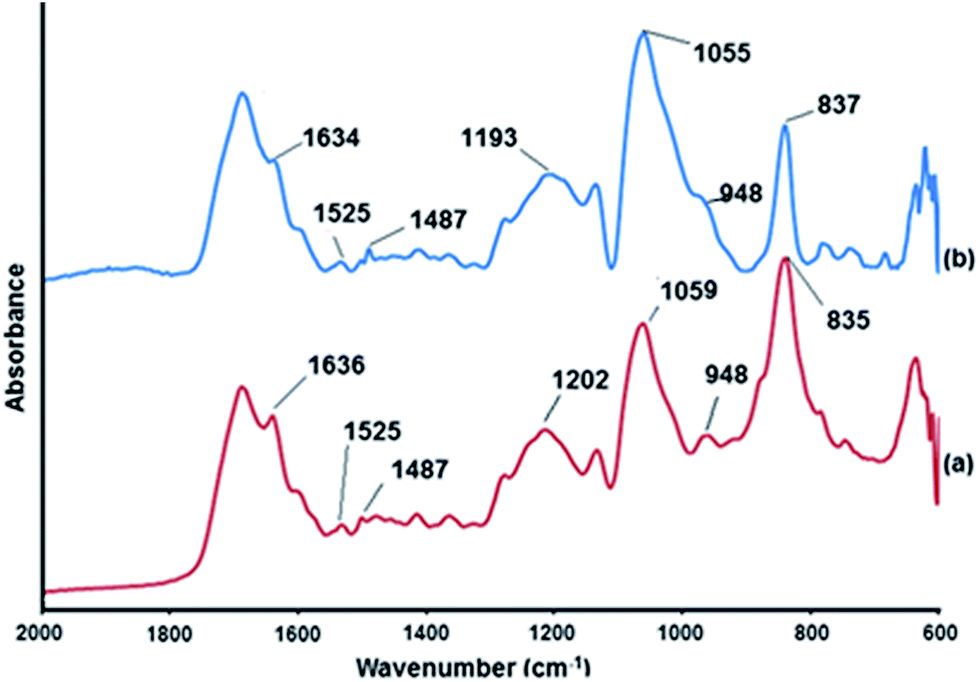 | ||
| Fig. 2 FTIR spectra of (a) polyNPPBH/DNA and (b) Cu/polyNPPBH/DNA hybrid structures in the 2000–600 cm−1 region. The spectra are offset on the y-axis for clarity. | ||
Bands observed in the 600–2000 cm−1 region of the spectrum confirm the presence of DNA in the hybrid material. These features can be assigned to nucleobase vibrations as well as stretches associated with the phosphate backbone. Changes in band positions and intensities are apparent for the nucleobase vibrations in the 1400–1800 cm−1 region of the spectra. Additionally, the CT-DNA spectrum shows a broad feature at 1096 cm−1 from PO2− symmetric stretches whereas a narrower band for this mode is observed at 1059 cm−1 for polyNPPBH/DNA which is shifted to lower frequency at 1055 cm−1 in Cu/polyNPPBH/DNA respectively. In general, the majority of the shifts in FTIR band positions observed are between bare DNA and polyNPPBH/DNA and that the differences in band positions/shapes between polyNPPBH/DNA and Cu/polyNPPBH/DNA are small (ESI, Table S1†). This suggests that the interaction of Cu with the underlying DNA is negligible and occurs dominantly with the polyNPPBH as expected. Further support for this interpretation comes from analysis of the AFM data below which shows that the polymer coating is thick and uniform on the template under the reaction conditions employed.
The presence of absorption bands located in the 600 to 650 cm−1 region in the FTIR spectrum of pure CT-DNA makes it difficult to assign if any peak corresponding to Cu(I)–O vibrations in the Cu/polyNPPBH/DNA sample spectrum, which is expected at ∼620 cm−1.27 However, the oxidation state of the Cu was determined to be mainly Cu(0) from the XPS data below. The intense infrared bands at 835 and 837 cm−1 for polyNPPBH/DNA and Cu/polyNPPBH/DNA samples respectively, are characteristic of the PF6− anion.28 No strong bands characteristic of NO3− (1460–1370 cm−1) were observed.
3.4 UV-vis absorption spectroscopy: formation of Cu/polyNPPBH/DNA
UV-vis absorption spectroscopy was employed to monitor the formation of Cu nanoparticles on polyNPPBH/DNA nanostructures. Ascorbic acid was chosen as the reducing agent following previous work.11 Electronic spectra of NPPBH, polyNPPBH, CT-DNA, polyNPPBH/DNA and Cu/polyNPPBH/DNA at room temperature in aqueous solution are shown in Fig. 3. In every case there is an absorption band in the UV region, but red-shifted compared to the characteristic absorption peak of CT-DNA at 260 nm (black curve, Fig. 3a).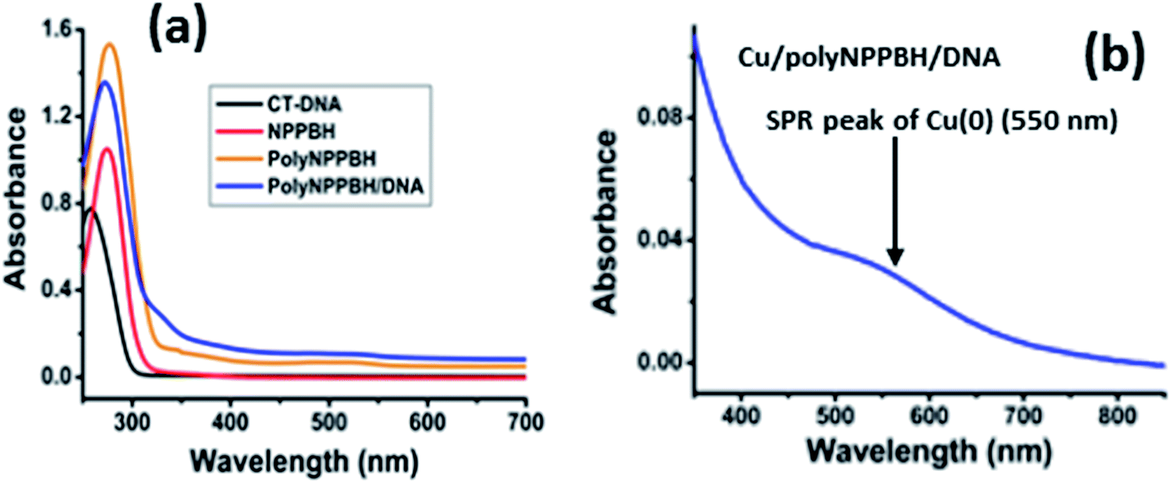 | ||
| Fig. 3 UV-vis absorption spectra of the Cu/polyNPPBH/DNA nanowires at different stages of the synthesis recorded at room temperature in aqueous solution. (a) UV-vis absorption spectra of CT-DNA (black curve), 5 mM NPPBH (red curve), polyNPPBH (orange curve) and polyNPPBH/DNA (curve blue). PolyNPPBH/DNA solution treated with Cu(NO3)2 and then reduced with ascorbic acid. Each curve is offset on the y-axis for clarity. (b) UV-vis absorption spectrum of Cu/polyNPPBH/DNA; the broad absorption band located around 550 nm is consistent with the surface plasmon resonance of metallic Cu. | ||
The UV absorption spectrum of NPPBH (red curve, Fig. 3a) shows a strong absorption band around 290 nm attributed to the n–π* transition. PolyNPPBH (orange curve, Fig. 3a) also displays an intense absorption at 290 nm; shoulders were observed in the range 360–380 nm in the polyNPPBH and polyNPPBH/DNA spectra which are assigned to π–π* transitions in the polymer backbone. The polyNPPBH and polyNPPBH/DNA spectra exhibit similar broad absorption bands around 480 nm assigned to the transitions from valence band to the polaron states in the gap. These features are not present in the monomer (red curve, Fig. 3a) but are characteristic of the polymer. PolyNPPBH/DNA solutions show a combination features due to DNA and polyNPPBH, but the peak positions are slightly shifted compared to the polyNPPBH spectrum indicating the sample is not a simple mixture of the two polymers.
Upon addition of ascorbic acid to a solution containing Cu2+ and polyNPPBH/DNA, the broad absorption for d–d transitions of Cu2+ in the range 700–900 nm disappears and a band at 550 nm is observed. The 550 nm band is consistent with the surface plasmon resonance of Cu nanostructures and provides evidence for the chemical reduction of Cu2+ to Cu0 in Cu/polyNPPBH/DNA.29,30
3.5 X-ray photoelectron spectroscopy
The C 1s, N 1s, Cu 2p1/2 and 2p3/2, O 1s, Cl 2p, and P 2p core-level photoemission spectra of Cu/polyNPPBH/DNA were recorded. The overall survey spectra obtained are shown in ESI.† The band in the P 2p spectrum at a binding energy of 132.1 eV corresponds to the phosphate group and indicates the presence of DNA molecules in the nanowires. The Cl 2p peak in the survey spectrum reveals the presence of the Cl− in the sample; this suggests that the anionic charge of the DNA is not sufficient to compensate the cationic charge of the bound polyNPPBH, and that Cl− anions are also present as dopants in the material. The survey scan shows a lack of Fe, and indicates that the oxidant FeCl3 is not incorporated to any significant extent, except as the source of Cl− present in the samples.The main features observed in the C 1s spectrum for Cu/polyNPPBH/DNA were at 284.6, 286.3, 288.2, and 289.1 eV (ESI†). Fitting of XPS Cu 2p spectrum reveals that two peaks located at 932.9 and 952.7 eV are respectively assigned to the binding energy of Cu 2p3/2 and Cu 2p1/2 (Fig. 4) in a good agreement with data observed for Cu0 nanowires.14 These two peaks are located with a separation of 19.8 eV which is in a good agreement with the established values for the Cu 2p1/2 and 2p3/2 splitting in metallic Cu0.31,32
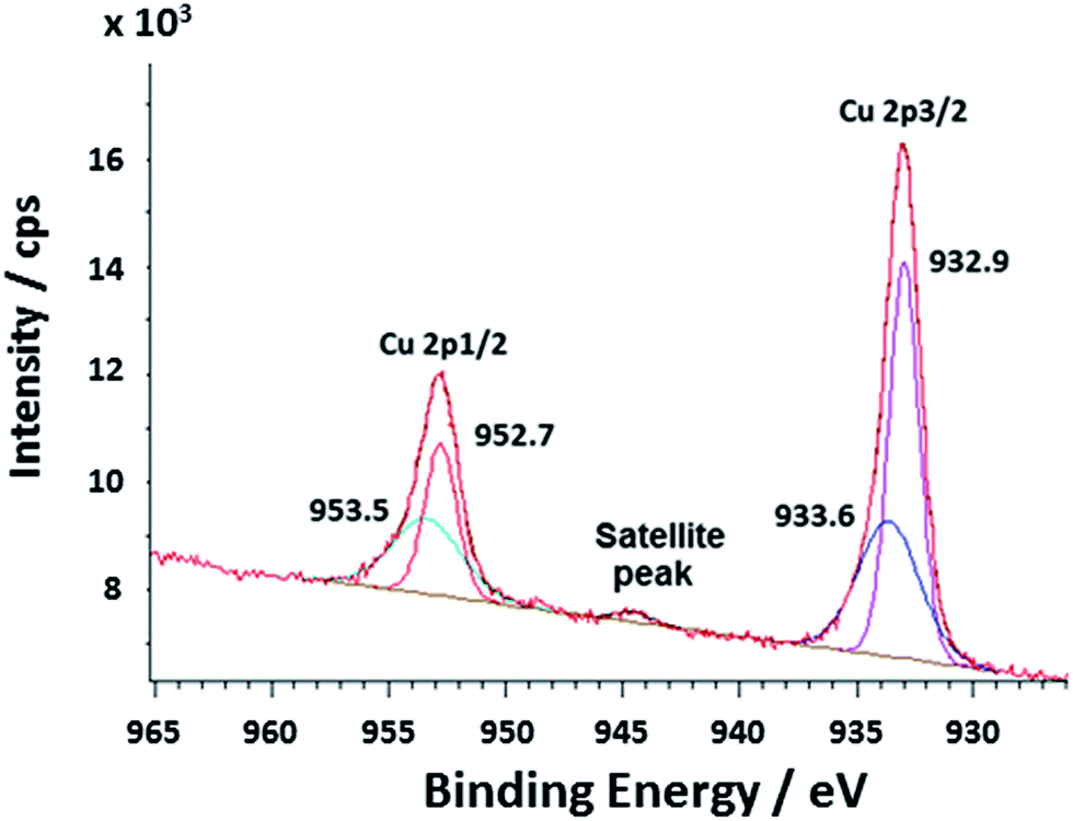 | ||
| Fig. 4 X-ray photoelectron spectra (Cu 2p region) of the Cu/polyNPPBH/DNA nanowires. Components due to Cu(0) and Cu(II) were observed in the deconvolution: the Cu 2p3/2 and Cu 2p1/2 peaks at 932.9 and 952.7 eV are attributed to Cu0. Two peaks detected at 933.6 and 953.5 eV are attributed to Cu2+. A weak satellite feature at about 944 eV is also assigned to Cu(II). The binding energies are reported after calibration of the energy scale so that the lowest DNA C 1s binding energy is 284.6 eV.33 | ||
Other peaks detected at 933.6 and 953.5 for Cu 2p3/2 and Cu 2p1/2 respectively are in agreement with previous reports on cupric oxide (CuO) and Cu(II) in general. The Cu 2p3/2–Cu 2p1/2 peak separation of 19.9 eV is typical of the CuO. In addition, the main peaks are relatively broad (3.4 eV) and accompanied with a satellite peak at about 9 eV higher binding energies which is absent in the case of Cu(I) samples, e.g., Cu2O.32 In Cu/polyNPPBH/DNA such a weak satellite feature was observed around 944 eV and is assigned to traces of unreacted Cu(II).
3.6 Atomic force microscopy of polyNPPBH/DNA and Cu/polyNPPBH/DNA
Structural characterisation of polymer/DNA nanowires is difficult by many conventional microscopy techniques, however AFM is effective because the nanowires can be combed on flat substrates to present the molecules in an aligned, uncoiled state.20 Such combing facilitates study of the nanowire diameters. Fig. 5 shows tapping mode AFM height images of the DNA-templated nanowires aligned on Si substrates after various reaction times. 2 hours after preparation (Fig. 5a) the polyNPPBH/DNA sample shows a mixture of very thin, bare DNA strands and thicker, but still smooth polyNPPBH/DNA strands. The polyNPPBH/DNA strands may comprise more than one DNA molecule (“ropes”) as can be seen on the left hand side of Fig. 5a, where there are clear branches in the structures.21 The polyNPPBH/DNA nanowires are continuous and, apart from the branch points, are uniform and have the same range of diameters (4–18 nm) along their length. Fig. 5b (after 24 h reaction time) shows thicker polyNPPBH/DNA nanowires, but also with uniform polymer coverage. In both Fig. 5a and b the substrate surface was mainly clear of untemplated polymer deposits. This data is consistent with our previous findings that conductive polymers produce regular and smooth nanowires when templated on λ-DNA by oxidative chemical polymerization.21,34,35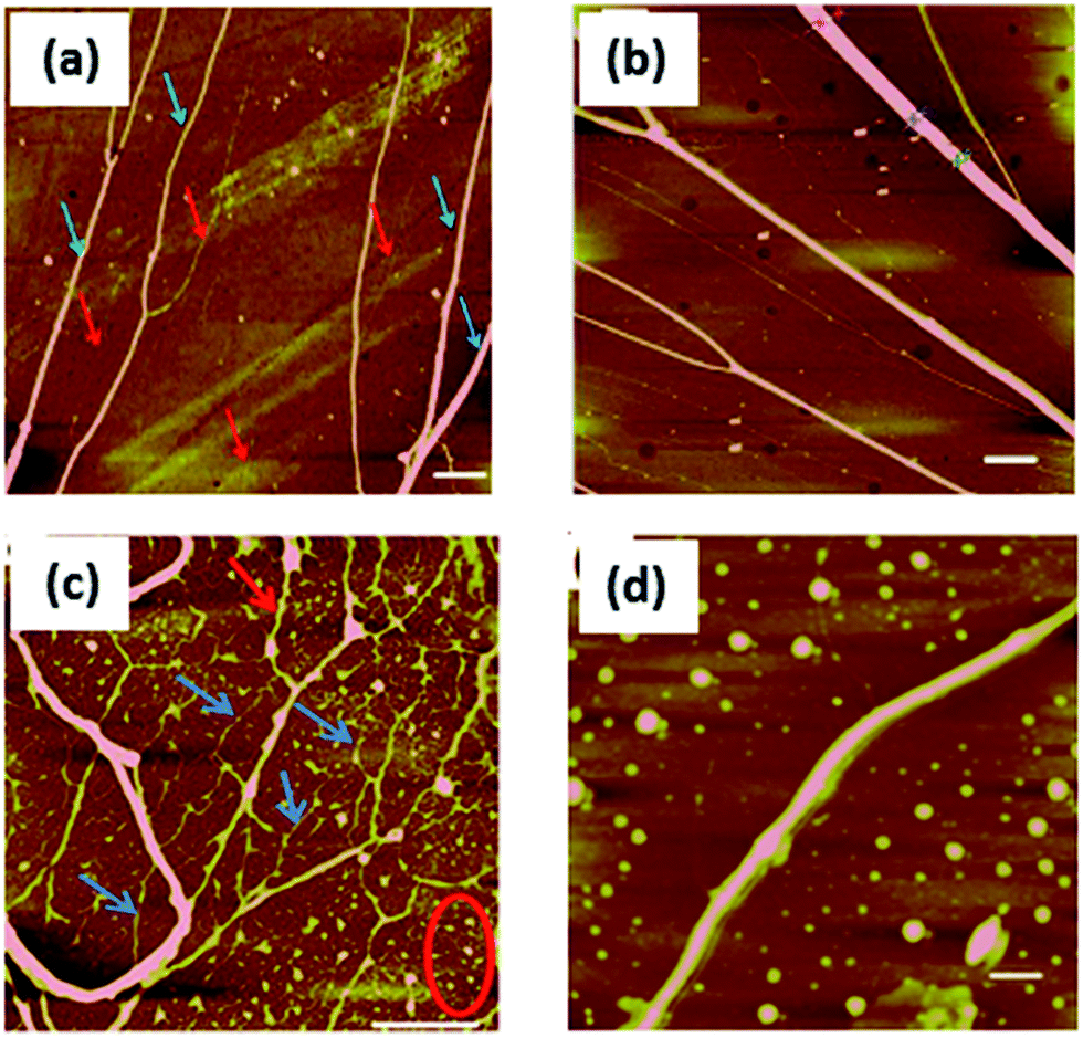 | ||
| Fig. 5 Tapping mode AFM images of polyNPPBH/DNA & Cu/polyNPPBH/DNA nanowires deposited on Si/SiO2 substrate after different incubation times (a) AFM height image of polyNPPBH/DNA nanowires after 2 h, the red arrows indicate the bare DNA molecules, where the blue arrows indicate the polymer/DNA nanowires. The gray scale corresponds to a height range of 10 nm; the scale bar is 1.0 μm. (b) Tapping mode AFM image of polyNPPBH/DNA nanorope after 24 h. The gray scale is 20 nm, and the scale bar is 1.0 μm. (c) Tapping mode AFM image of Cu/polyNPPBH/DNA nanowires after 24 h; scale bar is 1 μm, gray scale corresponds to 20 nm in height. (d) Tapping mode AFM image of Cu/polyNPPBH/DNA nanowires after 48 h, scale bar is 200 nm and the gray scale corresponds to 20 nm in height. | ||
Fig. 5c shows a Cu/polyNPPBH/DNA sample after addition of Cu2+ to polyNPPBH/DNA and reduction by ascorbate. Some segments appear thin or show breaks (examples indicated by blue arrows); this suggests incomplete coverage by Cu. Other strands (example indicated by red arrow) are relatively thicker, but with particles attached. Finally, there are many deposits on the substrate itself, not associated with a DNA template, examples are indicated by the red ellipse. These are likely to be Cu based on a comparison of Fig. 5c with 5a and b. Fig. 5d shows a Cu/polyNPPBH/DNA sample 24 h after addition of Cu2+ and ascorbate, i.e., after a total reaction time of 48 h. A more continuous metallization was achieved and resulted in relatively smooth metal-coated nanowires of 10–30 nm in diameter. However substantial deposition of Cu off-template was still observed and the metallized nanowires (Cu/polyNPPBH/DNA) are always rough compared with the case before metallization (polyNPPBH/DNA). Taken together these data suggest that the Cu deposits upon the polyNPPBH rather than the DNA.
Fig. 6 shows a histogram of heights of polyNPPBH/DNA nanowires 2 h after preparation. The mean diameter of the polyNPPBH/DNA (7.0 nm) was larger than that of bare DNA strands which was 2.6 nm including bundles of DNA and 1.5 nm including only single DNA molecules (ESI†). Based on these measurements, the thickness of the polymer coating (2.2–2.8 nm on average) is clearly greater than the radius of the DNA template and the polyNPPBH is the major component of the hybrid nanowires. However, we do also find that some bare DNA is present in the samples as indicated by the large number of structures with heights <3 nm. Larger heights, up to 18 nm, are also observed and some of these are likely to comprise multiple nanowires in a rope-like structure as observed for polypyrrole/DNA.21 Overall, there is a very broad range of heights, but this reflects variations between nanowires rather than variations of height along individual structures which are quite uniform (Fig. 5a and b). Finally, it is worth noting that the nanowires are generally longer than our maximum scan size which is expected if the integrity of the templated is not destroyed during the templating (λ-DNA is about 17 μm long). It is difficult to image or characterise the DNA itself after coating with polymer, however we have previously studied the effect of the oxidant FeCl3 on DNA molecules at millimolar concentrations and found no evidence of strand scission.35
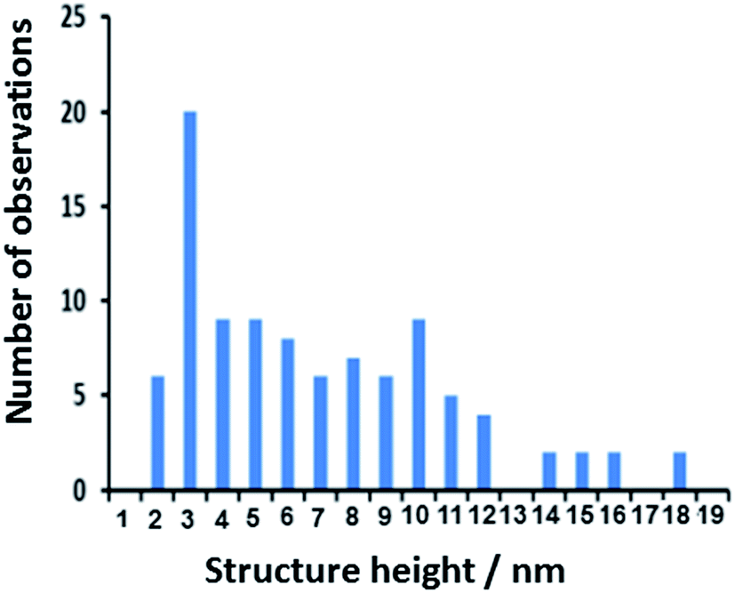 | ||
| Fig. 6 Height distribution of 100 polyNPPBH/DNA nanowires. The heights were determined from tapping mode AFM height images 2 h after preparation. It is also apparent from inspection of the histogram that not all the DNA in the reaction is involved in templating. This is evident from the peak observed at 2.0–3.0 nm, which mainly represents bare DNA that is present after the reaction. | ||
3.7 Electrical characterization of polyNPPBH/DNA and Cu/polyNPPBH/DNA using scanned conductance microscopy
SCM is a convenient method to make qualitative observations of the conductivity of nanoscale structures.36–38 It provides a simple, contactless technique to demonstrate the conductance of polymer/DNA nanowires. SCM is a dual-scan technique with a dc bias applied between a conductive tip and the substrate covered with a dielectric film (here SiO2) on which the nanowires lie. The sample topography is acquired in tapping mode during the first scan, the tip is then lifted at a defined height (tens of nm typ.) above the sample in the second scan and the phase shift between the mechanical drive and the cantilever oscillation is recorded. The phase-shift depends on the change in the effective spring constant, which is proportional to the second derivative of tip/substrate capacitance with respect to height. Topographical and electrical properties of the sample are therefore acquired in a single experiment. An easy distinction can be made between a bare DNA molecule (apparent height ∼ 1.5 nm, positive phase-shift in the SCM image) and that of a DNA molecule covered by conductive polymer or metal (diameter ≫ 1 nm, negative phase-shift in the SCM image). Insulating materials, whatever their polarisability, display a positive phase shift.36An SCM image of polyNPPBH/DNA nanowires (applied bias = +6 V and lift height 60 nm) is shown in Fig. 7a. The nanowires appear as dark lines (negative phase shift) compared to the insulating SiO2 surface, indicating that they are conductive. Bare DNA molecules (faint white lines show a positive phase shift indicating the absence of significant conductivity).
 | ||
| Fig. 7 (a) SCM phase image of polyNPPBH/DNA nanowires at a tip/sample bias of +6 V and lift height of 60 nm. The red arrow indicates non-covered parts of nanowires with positive phase shift. Scale bar = 500 nm. (a inset) The corresponding profile of the phase shift along a cross section of the nanowire at a diameter of 20 nm. (b) AFM image of a Cu/polyNPPBH/DNA nanowire after 24 h. (c) The corresponding SCM phase image at a tip/sample bias of +6 V and lift height of 60 nm. Scale bar of both images = 500 nm. (b inset) The height cross section of the nanowire, AFM image in (b), a diameter of ∼16 nm, (c inset) shows the corresponding profile of the phase shift along a cross section of the nanowire at a diameter of 16 nm. | ||
Parts of one nanowire shown in Fig. 7a (red arrow) appear incomplete, which is indicated by the lighter colour and a small positive phase shift. The profile of the phase shift along the cross-sections of the main nanowires, Fig. 7a inset, exhibits a W-shape, which is often observed for conducting polymers.8,21,37 Fig. 7b and c show topography and phase images of a thick Cu/polyNPPBH/DNA nanowire; as in Fig. 7a, the negative phase shift indicates a conductive structure and the W-shape of the phase profile across the nanowire is typical for conductive polymers. A few bare DNA strands with positive phase shift are also observed; this further confirms the role of the polyNPPBH in the sample conductivity. The untemplated material (blue circle, Fig. 7c) does not give a negative phase shift because objects of size comparable to the tip do not allow charge to flow away from the tip/sample region and do not have the same effect on the tip/sample capacitance as extended structures. The magnitude of the phase shift exhibits the expected parabolic dependence upon the sample bias – Fig. 8. This indicates that the data observed are mainly due to the conductance effect and the effect of the trapped charges, which generate a linear phase shift–bias relationship, may be ignored.
 | ||
| Fig. 8 (a) The phase shift of polyNPPBH/DNA nanowires as a function of applied tip bias voltage for different nanowires with different diameters. (b) The phase shift as a function of applied voltage for the Cu/polyNPPBH/DNA nanowire in Fig. 7b and c. | ||
3.8 Electrical characterization of polyNPPBH/DNA and Cu/polyNPPBH/DNA using conductive atomic force microscopy
Conductive AFM measurements of nanowires were made using the procedure previously described.8 In brief, a droplet of nanowires was allowed to dry on the substrate and individual nanowires are extended from the periphery of the dried material by surface forces. The tip makes contact to a single nanowire and the second (In/Ga) contact to complete the circuit is conveniently made to the mass of nanowires at the center of the dried droplet. The imaged area was about 1.0 mm away from the In/Ga eutectic contact. The mean diameter of the polyNPPBH/DNA nanowire in Fig. 9a was 15 nm. The closed loop system of the AFM instrument makes it possible to reproducibly position the cantilever at a point of interest on the nanowire and to record the current–voltage characteristic. The bias was swept from −5 to +5 V, while the deflection setpoint was maintained at 0.5 V. The zero-bias resistance was extracted from each of these linear characteristics and is plotted in Fig. 9 against the distance between the point at which the tip contacted the single nanowire and the edge of the main mass of nanowires. The same technique was applied to Cu/polyNPPBH/DNA nanowires. | ||
| Fig. 9 (a) PolyNPPBH/DNA nanowire resistance as a function of tip-contact relative distance in c-AFM measurements; sample bias = 7.0 V at 0.5 deflection set point. (b) Cu/polyNPPBH/DNA nanowire resistance at zero bias as a function of tip-contact relative distance at 0.5 V deflection set point. | ||
The variation of resistance against relative distance, d, of a polyNPPBH/DNA and a Cu/polyNPPBH/DNA nanowire is shown in Fig. 9. The resistance increases with d because the current must flow through a longer portion of the nanowire. The contact resistance at either the In/Ga contact or at the tip/nanowire contact is roughly independent of this distance, as evidenced by the linear plots. The resistivity of the nanowires can then be obtained directly from the slope of the plots of Fig. 9 after multiplying by the area of cross-section of each wire obtained from the height and width in the AFM image. We obtain values of conductivity of 0.42 ± 0.019 S cm−1 for the Cu/polyNPPBH/DNA nanowire and 2.1 ± 0.26 × 10⁻² S cm−1 for the polyNPPBH/DNA nanowire.
The conductivities of the nanowires illustrate several aspects of the conduction mechanism in these structures. First, there is a substantial (20-fold) increase upon metallization of polyNPPBH/DNA to make Cu/polyNPPBH/DNA. This stands in contrast to the case of Pd on polyimidazole/DNA structures where metallization had no significant effect on the conductivity of the polymer/DNA nanowire.10 The conduction pathway in Cu/polyNPPBH/DNA must therefore involve the Cu metallization. Second, the conductivity of Cu/polyNPPBH/DNA is less than of polypyrrole/DNA nanowires;21,39 this might be expected on the basis of the known bulk polyNPPBH conductivity, but it is worth noting that the conduction via the Cu metallization would not be detectable on a polypyrrole/DNA nanowire and in this respect the deleterious effect of the pyridine group on the polymer conductivity is advantageous in the present case. Finally, all these conductivity values are much lower than that of bulk Cu (∼6.0 × 10⁵ S cm−1 at 293 K).40 The nature of the conduction is therefore very different than in bulk metal and we suggest that a granular metal model41 is more appropriate for this kind of metal/polymer nanostructure.
4. Conclusion
Supramolecular polyNPPBH nanowires were fabricated using DNA as a template and electrically characterized. These nanowires were also used themselves as templates on which to form metallic Cu coatings by electroless deposition (Cu(NO3)2/ascorbate). The expected interaction between the anionic phosphate group of DNA and cationic polymer was indicated by FTIR which revealed changes in the vibration frequencies of the P–O stretching bands. The formation of metallic Cu was indicated by the surface plasmon resonance (SPR) peak near 550 nm in the visible spectrum and by the Cu 2p photoelectron spectra. Both polyNPPBH/DNA and Cu/polyNPPBH/DNA nanowires were found to be conductive. Using c-AFM, the conductivity of Cu/polyNPPBH/DNA nanowires was estimated at 0.42 ± 0.019 S cm−1, which is higher polyNPPBH/DNA nanowires (2.1 ± 0.26 × 10⁻² S cm−1). These results indicate some of the current flows through the Cu metallization in contrast to the case of palladium metallization on polyimidazole/DNA nanowires, i.e., Pd/polyimidazole/DNA.10Acknowledgements
Sebha University, Higher Education, Libya for sponsorship (MMA).References
- A. M. Morales and C. M. Lieber, Science, 1998, 279, 208–211 CrossRef CAS PubMed.
- C. Thelander, P. Agarwal, S. Brongersma, J. Eymery, L. F. Feiner, A. Forchel, M. Scheffler, W. Riess, B. J. Ohlsson, U. Gösele and L. Samuelson, Mater. Today, 2006, 9(10), 28–35 CrossRef CAS.
- S. Rahong, T. Yasui, N. Kaji and Y. Baba, Lab Chip, 2016, 16, 1126–1138 RSC.
- A. Houlton and S. M. D. Watson, Annu. Rep. Prog. Chem., Sect. A: Phys. Inorg. Chem., 2012, 107, 21–42 RSC.
- E. Braun, Y. Eichen, U. Sivan and G. Ben-Yoseph, Nature, 1998, 391(6669), 775–778 CrossRef CAS PubMed.
- Q. Huang, C. M. Lilley, M. Bode and R. Divan, J. Appl. Phys., 2008, 104(2), 023709 CrossRef.
- L. Dong, T. Hollis, B. A. Connolly, N. G. Wright, B. R. Horrocks and A. Houlton, Adv. Mater., 2007, 19(13), 1748–1751 CrossRef CAS.
- R. Hassanien, M. Al-Hinai, S. A. F. Al-Said, R. Little, L. Šiller, N. G. Wright, A. Houlton and B. R. Horrocks, ACS Nano, 2010, 4(4), 2149–2159 CrossRef CAS PubMed.
- R. Mas-Ballesté, O. Castillo, P. J. Sanz Miguel, D. Olea, J. Gómez-Herrero and F. Zamora, Eur. J. Inorg. Chem., 2009, 2009(20), 2885–2896 CrossRef.
- M. Al-Hinai, R. Hassanien, S. M. D. Watson, N. G. Wright, A. Houlton and B. R. Horrocks, Nanotechnology, 2016, 27(9), 095704 CrossRef PubMed.
- C. F. Monson and A. T. Woolley, Nano Lett., 2003, 3(3), 359–363 CrossRef CAS.
- J. Zhang, J. Sun, W. Liu, S. Shi, H. Sun and J. Guo, Nanotechnology, 2005, 16(10), 2030–2032 CrossRef CAS PubMed.
- H. Kudo and M. Fujihira, IEEE Trans. Nanotechnol., 2006, 5, 90–92 CrossRef.
- S. M. D. Watson, N. G. Wright, B. R. Horrocks and A. Houlton, Langmuir, 2010, 26(3), 2068–2075 CrossRef CAS PubMed.
- Y. Geng, A. C. Pearson, E. P. Gates, B. Uprety, R. C. Davis, J. N. Harb and A. T. Woolley, Langmuir, 2013, 29(10), 3482–3490 CrossRef CAS PubMed.
- J. Pate, F. Zamora, S. M. D. Watson, N. G. Wright, B. R. Horrocks and A. Houlton, J. Mater. Chem. C, 2014, 2(43), 9265–9273 RSC.
- S. A. F. Al-Said, R. Hassanien, J. Hannant, M. A. Galindo, S. Pruneanu, A. R. Pike, A. Houlton and B. R. Horrocks, Electrochem. Commun., 2009, 11(3), 550–553 CrossRef.
- B. R. Saunders, R. J. Fleming and K. S. Murray, Chem. Mater., 1995, 7(6), 1082–1094 CrossRef CAS.
- R. J. Waltman, A. F. Diaz and J. Bargon, J. Phys. Chem., 1984, 88(19), 4343–4346 CrossRef CAS.
- D. Bensimon, A. J. Simon, V. Croquette and A. Bensimon, Phys. Rev. Lett., 1995, 74, 4754–4757 CrossRef CAS PubMed.
- S. Pruneanu, S. A. F. Al-Said, L. Dong, T. A. Hollis, M. A. Galindo, N. G. Wright, A. Houlton and B. R. Horrocks, Adv. Funct. Mater., 2008, 18(16), 2444–2454 CrossRef CAS.
- S. Cosnier, A. Deronzier, J. C. Moutet and J. F. Roland, J. Electroanal. Chem., 1989, 271(1–2), 69–81 CrossRef CAS.
- J. Heinze, Synth. Met., 1991, 43(1–2), 2805–2823 CrossRef CAS.
- A. F. Diaz, J. Castillo, K. K. Kanazawa, J. A. Logan, M. Salmon and O. Fajardo, J. Electroanal. Chem., 1982, 133(2), 233–239 CrossRef CAS.
- K. Takada, Z. Naal and H. D. Abruña, Langmuir, 2003, 19(13), 5402–5406 CrossRef CAS.
- G. Han, G. Shi, J. Yuan and F. Chen, J. Mater. Sci., 2004, 39(14), 4451–4457 CrossRef CAS.
- B. Balamurugan and B. R. Mehta, Thin Solid Films, 2001, 396(1–2), 90–96 CrossRef CAS.
- P. W. Hansen and P. W. Jensen, Spectrochim. Acta, Part A, 1994, 50(1), 169–183 CrossRef.
- A. Henglein, J. Phys. Chem. B, 2000, 104, 1206–1211 CrossRef CAS.
- J. L. Duan, T. W. Cornelius, J. Liu, S. Karim, H. J. Yao, O. Picht, M. Rauber and S. Müller, J. Phys. Chem. C, 2009, 113(31), 13583–13587 CAS.
- C. D. Wagner, W. M. Riggs, L. E. Davis and J. F. Moulder, Handbook of X-Ray Photoelectron Spectroscopy, Perkin-Elmer, Ramsey, MN, 1979 Search PubMed.
- J. C. Fuggle, E. Kallne, L. M. Watson and D. J. Fabian, Phys. Rev. B: Condens. Matter Mater. Phys., 1977, 16, 750–761 CrossRef CAS.
- S. Ptasinska, A. Stypczynska, T. Nixon, N. J. Mason, D. V. Klyachko and L. Sanche, J. Chem. Phys., 2008, 129, 065102 CrossRef PubMed.
- S. M. D. Watson, M. A. Galindo, B. R. Horrocks and A. Houlton, J. Am. Chem. Soc., 2014, 36, 6649–6655 CrossRef PubMed.
- L. Dong, T. Hollis, S. Fishwick, B. A. Connolly, N. G. Wright, B. R. Horrocks and A. Houlton, Chem.–Eur. J., 2007, 13, 822–828 CrossRef CAS PubMed.
- C. Staii, A. T. Johnson and N. J. Pinto, Nano Lett., 2004, 4(5), 859–862 CrossRef CAS.
- T. S. Jespersen and J. Nygard, Nano Lett., 2005, 5(9), 1838–1841 CrossRef CAS PubMed.
- M. Bockrath, N. Markovic, A. Shepard, M. Tinkham, L. Gurevich, L. P. Kouwenhoven, M. W. Wu and L. L. Sohn, Nano Lett., 2002, 2, 187–190 CrossRef CAS.
- L. Dong, T. Hollis, S. Fishwick, B. A. Connolly, N. G. Wright, B. R. Horrocks and A. Houlton, Chem.–Eur. J., 2007, 13, 822–828 CrossRef CAS PubMed.
- R. Matula, J. Phys. Chem. Ref. Data, 1979, 8(4), 1147–1298 CrossRef CAS.
- P. Sheng, B. Abeles and Y. Arie, Phys. Rev. Lett., 1973, 31, 44–47 CrossRef CAS.
Footnote |
| † Electronic supplementary information (ESI) available: (i) Synthesis of the NPPBH monomer; (ii) FTIR data for NPPBH, polyNPPBH and polyNPPBH/DNA; (iii) UV-vis absorption spectra for NPPBH and polyNPPBH; (iv) additional photoelectron (XPS) spectra for Cu/polyNPPBH/DNA nanowires and (v) AFM height data for bare DNA molecules for comparison with nanowires. See DOI: 10.1039/c6ra20325f |
| This journal is © The Royal Society of Chemistry 2016 |