Well-defined quantum dots and broadening of optical phonon line from hydrothermal method

Deepika Jamwal a, Dolly Ranaa, Pardeep Singha, Dinesh Pathak*b, Susheel Kaliac, Pankaj Thakur*ad and Enza Torinod
aSchool of Chemistry, Faculty of Basic Sciences, Shoolini University, Solan, HP 173212, India. E-mail: chempank@gmail.com
bFaculty of Chemical Technology, University of Pardubice, Pardubice 53210, Czech Republic. E-mail: dineshpathak80@gmail.com
cDepartment of Chemistry, Army Cadet College Wing, Indian Military Academy Dehradun, UK 248007, India
dIstituto Italiano di Tecnologia (Center for Advanced Biomaterials for Healthcare), Naples 80125, Italy

Received 5th August 2016 , Accepted 24th September 2016

First published on 10th October 2016


Abstract

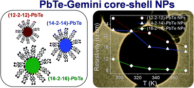
A versatile and facile methodology is presented for size-controlled, lead telluride nanoparticles in the presence of highly hydrophobic cationic gemini surfactants (12–2–12, 14–2–14 and 16–2–16) as capping/stabilizing agents. The optical and electrical properties were examined with attention focused on the cumulative diameter of lead telluride NPs for various stabilizing agents. To explore the influence of surfactants' hydrophobicity on the shape and size of lead telluride NPs, the microstructure of lead telluride NPs was investigated via transmission electron microscopy (TEM). Core–shell nanoparticles were characterized by using XRD, near-IR, PL and Raman techniques.


Semiconductor nanocrystals with various sizes and architectures may open new opportunities for exploring their physical and chemical properties, and great effort has been devoted to controlling the material's size, shape, and dimensions.1,2 In particular, inorganic semiconductor quantum dots are attractive candidates with their unique properties that may be useful for a variety of applications such as electrochromic displays,3,4 optical recording materials,5 optical filters,6 light-emitting diodes7 and protein assays.8 In recent years, several research efforts has been focused on semiconductor nanocrystals because of quantum confinement effects and related potential applications.9 The size tunable optical and electronic properties of semiconductor nanoparticles derive from synthesis of quantum dots with radii comparable to or smaller than the Bohr exciton radius. Binary IV–VI semiconducting compounds are particularly interesting because of potential applications. As a narrow-band-gap semiconductor (0.32 eV) and face-centred cubic (rock salt) structure, lead telluride (PbTe) has been extensively studied and explored for applications in infrared photovoltaics,10,11 optical switches,12 laser devices,13 photodetectors14 and thermoelectrics,15 Compared to other semiconductor materials, low-dimension PbTe semiconductors could more easily show obvious quantum size effects on larger scales because of the larger Bohr exciton radius (about 46 nm).16 At dimensions comparable with the Bohr exciton radius, quantum confinement makes the properties of lead telluride more exotic. Size- and shape-controlled morphologies are the common building blocks for nanodevices. The conventional surfactants such as cetyltrimethylammonium bromide (CTAB), polyvinylpyrrolidone (PVP), sodium dodecyl sulphate (SDS) and dodecyltrimethylammonium bromide (DTAB) have been used for designing different morphologies and controlling the size.17–19 Surfactant-assisted synthesis is environmentally friendly and reproducible and produces high yields. Surfactant structure—comprised of one hydrophilic and one hydrophobic chain each—kinetically controls growth rates of different crystallographic facets of nanoparticles through preferentially adsorbing and desorbing on these facets.20

Gemini surfactants are a relatively new class of surfactants that have two hydrophobic chains (m) and two polar head groups combined by a covalently bonded spacer group (s), which may be of variable length (m–s–m). They have attracted much attention due to features that conventional surfactants lack, such as low critical micelles concentration, good water solubility, low Kraft point and excellent surface activity in aqueous solution. The gemini variety has great potential as a new tool for nanoparticle shape and size control.21,22 In this work, we propose a simple one-step hydrothermal method for preparing shape- and size-controlled lead telluride quantum dots using diverse gemini surfactants. Based on our very recent experience with CuTe & PbTe NPs in the presence of a gemini surfactant—that is, 12–2–12—, we developed an array of gemini surfactant-covered PbTe nanoparticles20 to gain deeper understanding of the surfactant-controlled hydrothermal synthetic process. In brief, 10 mL of aqueous gemini surfactant solutions of a stipulated concentration containing 2.5% hydrazine was placed in a conical flask, followed by 15 mL of 1 mM lead acetate and then 1 M NaOH. Thereafter, 10 mL of 1 mM sodium telluride solution was added, and then the mixture was diluted to 40 mL under constant stirring for 10 min. The clear solution was transferred into a Teflon-lined autoclave with a volume capacity of 50 mL, up to 80% capacity of the autoclave's capacity. The sealed autoclave was put into a 150 °C furnace for 32 h. Subsequently, the container was cooled to room temperature. The grey powder was collected by centrifuging at 4500 rpm and washed several times with distilled water and ethanol to obtain the purified sample.

The powder X-ray diffraction (XRD) patterns for the lead telluride nanoparticles synthesized at 150 °C in the presence of an array of gemini surfactants are presented in Fig. 1(a). Peaks corresponding to (200), (221), (220), (222), (400), (420) and (422) demonstrate Bragg reflections at the cubic phase of lead telluride nanoparticles.23 For estimating the average nanoparticle size using X-ray diffraction measurements, Scherrer's equation is the most common method. Based on diverse theta values, the average particle size for lead telluride nanoparticles with gemini surfactants—that is, (12–2–12), (14–2–14) and (16–2–16)—was calculated about 29.53 nm, 32.17 nm and 39.12 nm, respectively.


image file: c6ra19818j-f1.tif
Fig. 1 (a) XRD pattern of PbTe nanoparticles capped with different gemini surfactants. (b)–(d) Show TEM images of PbTe NPs synthesized with different surfactants (12–2–12), (14–2–14) and (16–2–16), respectively.

Fig. 1(b)–(d) present transmission electron micrographs of lead telluride nanoparticles overlaid with different gemini surfactants obtained at 150 °C under hydrothermal conditions. TEM images show similar morphologies in the presence of different gemini surfactants, the smaller nanoparticles with average diameters of 50 ± 15.18 nm have been observed with smallest gemini surfactant i.e. (12–2–12) and the average diameter of lead telluride nanoparticles goes on increasing with increase in the length of gemini surfactants. The average diameter for (14–2–14) and (16–2–16) capped nanoparticles has been found to be 65 ± 18.70 nm and 85 ± 18.7 nm respectively. Histograms of the nanoparticles that correspond to the TEM images are shown in Fig. S1(a)–(c). The XRD pattern shows (200) peak with higher intensity as compared to other peaks for lead telluride nanoparticles capped with different geminis and this intensity is increased with increase in the tail length of the surfactants which suggest the texture of the material in (200) direction. Fourier transform infrared (FTIR) spectroscopic measurements were performed to demonstrate whether the lead telluride nanoparticles are undeniably capped by gemini surfactants. In FTIR measurements, lead telluride capped by gemini surfactants were compared with the corresponding pure surfactant's IRs (Fig. S2).

The near-IR region absorption spectra of gemini surfactant-capped PbTe nanoparticles appears in Fig. 2(a). Absorption peaks for lead telluride nanoparticles were found in the 1200 nm–2800 nm range. From nucleation to growth and stabilization, the role of the capping agent seems crucial for nanoparticle synthesis. We observed an increase in particle size as the tail length of gemini surfactants was increased. The ability to control particle size is of fundamental importance in preparing high-quality lead telluride nanoparticles and particularly their optical properties. Capacity to modify size effects in such a system makes possible the tuning its exceptional properties to specific applications. Quantum confinement effects are clearly observed as shown by the blue shift of the respective peaks. The appearance of sharp peaks in absorption spectra demonstrates the high quality of the synthesized samples. The optical band gap energy of nanoparticles was calculated using the Tauc relation.24 The band gap energy of bulk PbTe is 0.32 eV. The blue shift of 0.42, 0.43 and 0.45 eV of (16–2–16), (14–2–14) and (12–2–12) capped nanoparticles, respectively, is the result of quantum confinement (Fig. 2(b)–(d)). As the size of quantum dots becomes smaller and approaches the exciton Bohr radius, quantum confinement effects occur and a blue shift in exciton energy can be observed.25 The blue shift progressively decreases with cumulative particle diameter and the optical band gap of semiconductor nanoparticles. The electrochemical band gap from the diverse anodic and cathodic peaks from Fig. S3 is calculated as 0.44, 0.41 and 0.35 eV for (12–2–12), (14–2–14) and (16–2–16) capped lead telluride nanoparticles, respectively, which is close to the values obtained spectroscopically.


image file: c6ra19818j-f2.tif
Fig. 2 (a) Shows near-IR spectrum. (b)–(d) Show Tauc plots for lead telluride NPs; dotted lines represent extrapolation for band gap.

Measurement of photoluminescence (PL) spectra was performed at room temperature. Fig. 3(a) shows the PL spectra of prepared lead telluride nanoparticles. Photoluminescence is a two-step process consisting of absorption of incoming photons by electrons and emission of outgoing photons by thermalized electrons. As a result of thermalization, the outgoing photon is not coherent with the incoming photon. Typically two emissions can be perceived from semiconductor nanomaterials: one is the acute excitonic emission located near the absorption band edge and another is the broad emission due to surface states or defects.26,27 Lead telluride nanoparticles exhibit a strong peak around 813 nm and a broad emission peak around 649 nm. The hydrothermal treatment of lead telluride nanoparticles in the presence of (12–2–12), (14–2–14) and (16–2–16) gemini surfactants results in the narrowing of the PL band, making them better for selective colour emission and increased intensity by an order of magnitude. It is worthwhile noting that increase in tail length of gemini surfactants also resulted in increased PL intensity. The broadening of PL emission peaks was observed as nanoparticle diameter decreased for (16–2–16), (14–2–14) and (12–2–12) capped NPs, respectively. This broadening of the PL peak can be attributed to strain in nanoparticles caused by size-induced quantization effects. The defects or strain/stress are imported in the NPs due to quantum confinement effects at the nanoscale.23 Both absorption and photoluminescence properties suggest that these nanoparticles may be used for third-generation quantum dot solar cells and other devices.


image file: c6ra19818j-f3.tif
Fig. 3 (a) Photoluminescence. (b) Raman spectra of lead telluride nanoparticles capped with (12–2–12), (14–2–14) and (16–2–16) gemini surfactants.

PbTe nanoparticles prepared were further characterized by Raman spectroscopy; the Raman spectra obtained are presented in Fig. 3(b). Spectra exhibited by the bands at 73 and 182 cm−1 for (12–2–12), and at 73 and 103 cm−1 for both (14–2–14) and (16–2–16) capped NPs may be due to the phonon modes of lead telluride used at different critical points of the Brillouin zone.28 Meanwhile, the peak at around 725 cm−1 for (12–2–12) and at 692 cm−1 in the cases of (14–2–14), (16–2–16) capped PbTe NPs were attributed to ground state energy of the polaron.29,30 In the current system, the shift of some bands towards lower as well as higher wavelength sides may be associated with the shape of dispersion of the lattice phonon with a maximum wavelength at the zone centre, which decreases as the phonon vector moves towards the zone edges. The confinement of phonons, optical as well as acoustic, evidently influences the phonon spectra when grain size falls to the nanometer range. Quantum confinement of the optical phonon causes asymmetry in the line shape and a shift towards the low frequency side compared to that for bulk lead telluride.31 Therefore, it is proposed that the optical phonon line will also get broadened with the decrease in size. This broadening may also arise from the disorder present in lead telluride nanoparticles due to quantum confinement effects.32

Recent works on electrical properties of semiconductor nanoparticles focused considerable attention on the conduction mechanism. Electrical conductivity of lead telluride NPs occurred in the range of 293–373 K. Electrical conductivity can be altered by adjusting the size of electricity-conducting material as the particle size plays an significant role in conductivity. Increased confinement may cause reduced overall available density of states leading to a drop in electrical conductivity.33,34 The synthesized lead telluride nanoparticles exhibit a linear current–voltage (IV) curve that is symmetric about the origin (Fig. 4(a)–(c)). The current increases linearly with voltage, which implies that conduction is ohmic. The resistance of lead telluride samples at different temperatures was calculated from the slope of the IV curve. Fig. 4 illustrates temperature dependence of electrical resistivity for (12–2–12), (14–2–14) and (16–2–16) capped lead telluride nanoparticles, which varies for different lead telluride nanoparticle as (25.89–16.34 Ω cm), (22.05–14.55 Ω cm) and (12.01–8.06 Ω cm), respectively, at different temperatures (293–373 K). On account of resistance and size, including length, width and thickness of samples, the electrical conductivities of lead telluride NPs were measured at 0.04–0.06 S cm−1, 0.05–0.07 S cm−1 and 0.08–0.12 S cm−1 for (12–2–12), (14–2–14) and (16–2–16) capped NPs, respectively. The lead telluride nanoparticles have good conductivity with increasing temperature, which displays semiconductor conductance.35,36 The curve obtained for electrical conductivity in NPs is in excellent agreement with available experimental data.37,38 In our experiments, observed values of conductivity at different temperatures for lead telluride core–shell nanoparticles were found to be greater than in previous reported results.36,39 Strong dependence of electrical conductivity on the size and shape parameters of NPs creates an opportunity for re-engineering of optical, electronic and thermal properties of this nanostructure through modification.


image file: c6ra19818j-f4.tif
Fig. 4 (a)–(c) IV characteristics at different temperatures and (d) variation of resistivity with temperature for (12–2–12), (14–2–14) and (16–2–16) stabilized lead telluride NPs.

In this study, we employed gemini surfactants (12–2–12, 14–2–14 and 16–2–16) with a short spacer length, that is, s = 2; the two heads with smaller spacer length were constantly drawn close and accordingly the adsorbed molecules are packed more tightly in comparison to conventional molecules. On the basis of critical micelle concentration range, 16–2–16 was found to be more hydrophobic in contrast to 14–2–14 and 12–2–12 surfactants, resulting in excellent capping ability and stronger liquid–solid interfacial adsorption. Increased hydrophobicity of surfactants from (12–2–12) to (16–2–16) therefore led to increased size of lead telluride nanoparticles.40–43 Size-controlled synthesis of lead telluride nanoparticles was successfully realized via a simple hydrothermal route employing an array of gemini surfactants. Hydrophobicity is recognized as the main size-governing factor as evidenced by TEM images. The average diameter of lead telluride nanoparticles is 50 ± 15.18, 65 ± 18.70 and 85 ± 18.7 nm for (12–2–12), (14–2–14) and (16–2–16), respectively. Raman spectra of nanoparticles confirmed the presence of PbTe phases. The near-IR studies revealed that the optical band gap increases as the size of the nanoparticles decreases, which shows blue shift due to quantum confinement at the nanoscale. The optical band gap is found to be 0.42, 0.43 and 0.45 eV for 50 ± 15.18, 65 ± 18.70 and 85 ± 18.7 nm lead telluride nanoparticles, respectively, and exhibits a strong photoluminescence peak around 813 nm and a broad emission peak around 649 nm. Electrical conductivities of lead telluride NPs have been measured to be 0.04–0.06 S cm−1, 0.05–0.07 S cm−1 and 0.08–0.12 S cm−1 for (12–2–12), (14–2–14) and (16–2–16) capped NPs, respectively. Lead telluride nanoparticles have good conductivity with increasing temperature, which displays semiconductor conductance.

Acknowledgements

The authors are indebted to the Vice Chancellor, Shoolini University of Biotechnology & Management Sciences, Solan, India for providing basic laboratory amenities. D. J. and D. R. equally share first authorship.

Notes and references

  1. S. G. Kwon and T. Hyeon, Acc. Chem. Res., 2008, 41, 1696–1709 CrossRef CAS PubMed.
  2. V. I. Klimov, A. A. Mikhailovsky, S. Xu, A. Malko, J. A. Hollingsworth, C. A. Leatherdale, H. J. Eisler and M. G. Bawendi, Science, 2000, 290, 314–317 CrossRef CAS PubMed.
  3. S. Coe, W. K. Woo, M. Bawendi and V. Bulovic, Nature, 2002, 420, 800–803 CrossRef CAS PubMed.
  4. M. Ji, S. Park, S. T. Connor, T. Mokari, Y. Cui and K. J. Gaffney, Nano Lett., 2009, 9, 1217–1222 CrossRef CAS PubMed.
  5. M. Wang, G. Fang, L. Yuan, H. Huang, Z. Sun, N. Liu, S. Xia and X. Zhao, Nanotechnology, 2009, 20, 185304 CrossRef PubMed.
  6. M. S. Bakshi, P. Thakur, G. Kaur, H. Kaur, T. S. Banipal, F. Possmayer and N. O. Petersen, Adv. Funct. Mater., 2009, 19, 1451–1458 CrossRef CAS.
  7. M. S. Bakshi, P. Thakur, S. Sachar and T. S. Banipal, Mater. Lett., 2007, 16, 3762–3773 CrossRef.
  8. T. C. Harman, P. J. Taylor, M. P. Walsh and B. E. LaForge, Science, 2002, 297, 2229–2232 CrossRef CAS PubMed.
  9. M. Fardy, A. I. Hochbaum, J. Goldberger, M. M. Zhang and P. Yang, Adv. Mater., 2007, 19, 3047–3051 CrossRef CAS.
  10. E. H. Sargent, Adv. Mater., 2005, 17, 515–522 CrossRef CAS.
  11. P. Singh, P. Raizada, S. Kumari, A. Kumar, D. Pathania and P. Thakur, Appl. Catal., A, 2014, 476, 9–18 CrossRef CAS.
  12. A. S. Barros, E. Abramof and P. H. O. Rappl, J. Appl. Phys., 2006, 99, 024904 CrossRef.
  13. F. W. Wise, Acc. Chem. Res., 2000, 33, 773–780 CrossRef CAS PubMed.
  14. Z. Feit, D. Kostyk, R. J. Woods and P. Mak, Appl. Phys. Lett., 1991, 58, 343–345 CrossRef CAS.
  15. F. M. Hochbaum, A. I. Goldberger, J. Zhang and P. Yang, Adv. Mater., 2007, 19, 3047–3051 CrossRef.
  16. B. Poudel, W. Z. Wang, D. Z. Wang, J. Y. Huang and Z. F. Ren, J. Nanosci. Nanotechnol., 2006, 6, 1050–1053 CrossRef CAS PubMed.
  17. S. M. Yong, P. Muralidharan, D. S. Kim and D. K. Kim, Rev. Adv. Mater. Sci., 2011, 28, 13–16 CAS.
  18. E. Torino, R. Aruta, T. Sibillano, C. Giannini and P. A. Netti, Sci. Rep., 2016, 6, 1–12 Search PubMed.
  19. G. Bai, J. Wang, H. Yan, Z. Li and R. K. Thomas, J. Phys. Chem. B, 2001, 105, 3105–3108 CrossRef CAS.
  20. T. Jain, A. R. Tehrani-Bagha, H. Shekhar, R. Crawford, E. Johnson, K. Norgaard, K. Holmberg, P. Erhartc and K. Moth-Poulsen, J. Mater. Chem. C, 2014, 2, 994–1003 RSC.
  21. Z. Quan, C. Li, X. Zhang, J. Yang, P. Yang, C. Zhang and J. Lin, Cryst. Growth Des., 2008, 8, 2384–2392 CAS.
  22. M. S. Bakshi, F. Possmayer and N. O. Petersen, Chem. Mater., 2007, 19, 1257–1266 CrossRef CAS.
  23. D. Jamwal, G. Kaur, P. Raizada, P. Singh, D. Pathak and P. Thakur, J. Phys. Chem. C, 2015, 119, 5062–5073 CAS.
  24. J. Tauc, R. Grigorovici and A. Vancu, Phys. Status Solidi B, 1996, 15, 627–637 CrossRef.
  25. L. E. Brus, J. Chem. Phys., 1984, 80, 4403–4409 CrossRef CAS.
  26. R. Kripal, A. K. Gupta, S. K. Mishra, R. K. Srivastava, A. C. Pandey and S. G. Prakash, Spectrochim. Acta, Part A, 2010, 76, 523–530 CrossRef PubMed.
  27. M. A. Zwijnenburg, Nanoscale, 2012, 4, 3711–3717 RSC.
  28. S. P. Zimina, E. S. Gorlacheva, A. V. Baranovc, S. A. Cherevkovc, E. Abramofd and P. H. O. Rappld, Opt. Spectrosc., 2014, 117, 748–752 CrossRef.
  29. R. Romano-Trujillo, E. Rosendo, M. Ortega, A. Morales-Sanchez, J. M. Gracia, T. Diaz, G. Nieto, G. Garcia, J. A. Luna-Lopez and M. Pacio, Nanotechnology, 2012, 23, 185602 CrossRef CAS PubMed.
  30. T. Huang and L. Qi, Nanotechnology, 2009, 20, 025606 CrossRef PubMed.
  31. R. R. Prabhu and M. A. Khadar, Bull. Mater. Sci., 2008, 31, 511–515 CrossRef CAS.
  32. V. M. Fomin, E. P. Pokatilov, J. T. Devreese, S. N. Klimin, V. N. Gladilin and S. N. Balaban, Solid-State Electron., 1998, 42, 1297–1309 CrossRef.
  33. Y. Son, M. Park, Y. Son, J. S. Lee, J. H. Jang, Y. Kim and J. Cho, Nano Lett., 2014, 14, 1005–1010 CrossRef CAS PubMed.
  34. M. S. Dresselhaus, G. Chen, M. Y. Tang, R. Yang, H. Lee, D. Wang, Z. Ren, J. P. Fleurial and P. Gogna, Adv. Mater., 2007, 19, 1043–1053 CrossRef CAS.
  35. V. F. Kharlamov, D. A. Korostelev, I. G. Bogoraz, O. A. Milovidova and V. O. Sergeyev, Semiconductors, 2013, 47, 494–500 CrossRef CAS.
  36. L. Kungumadevi and R. Sathyamoorthy, Adv. Powder Technol., 2013, 24, 218–223 CrossRef CAS.
  37. W. Wana, C. Hu, B. Feng, Y. Xi and X. He, Mater. Sci. Eng., B, 2009, 163, 57–61 CrossRef.
  38. G. Tai, W. Guo and Z. Zhang, Cryst. Growth Des., 2008, 8, 2906–2911 CAS.
  39. Y. Y. Wang, K. F. Cai and X. Yao, J. Solid State Chem., 2009, 182, 3383–3386 CrossRef CAS.
  40. W. Chang, Y. Shen, A. Xie, H. Zhang, J. Wanga and W. Lu, J. Colloid Interface Sci., 2009, 335, 257–263 CrossRef CAS PubMed.
  41. M. S. Bakshi, K. Singh, G. Kaur, T. Yoshimura and K. Esumi, Colloids Surf., A, 2006, 278, 129–139 CrossRef CAS.
  42. P. Sharma, S. Sachar, G. Kaur, P. Thakur, M. S. Bakshi and T. S. Banipal, J. Surf. Sci. Technol., 2007, 23, 131–147 CAS.
  43. P. Singh, P. Raizada, D. Pathania, A. Kumar and P. Thakur, Int. J. Photoenergy, 2013, 2013, 726250 CrossRef.

Footnotes

Electronic supplementary information (ESI) available. Fig. S1 FTIR spectra of (a) pure gemini surfactants and (b) PbTe NPs synthesized with (12-2-12), (14-2-14) and (16-2-16) gemini surfactants. Fig. S2 cyclic voltammetric studies for lead telluride nanoparticles. See DOI: 10.1039/c6ra19818j
D.J. and D.R. equally share first authorship.

This journal is © The Royal Society of Chemistry 2016