
A flexible sandwich graphene/silver nanowires/graphene thin film for high-performance electromagnetic interference shielding
Pradip Kumar*ab,
Faisal Shahzadac,
Soon Man Hongac and
Chong Min Koo*ac
aCenter for Materials Architecturing, Korea Institute of Science and Technology, Seongbuk-gu, Seoul 136791, Republic of Korea. E-mail: koo@kist.re.kr
bChemistry Division, Bhabha Atomic Research Centre, Trombay, 400085, Mumbai, India. E-mail: pradipk@barc.gov.in
cNanomaterials Science and Engineering, University of Science and Technology, Yuseong-gu, Daejeon 305350, Republic of Korea
First published on 13th October 2016
Abstract
We report the preparation and characterization of flexible graphene/silver nanowires (AgNWs)/graphene sandwich thin films for high-performance electromagnetic interference shielding. AgNWs were sandwiched between reduced graphene oxide (rGO) films through a simple filtration process followed by reduction with hydriodic acid. The rGO/AgNWs/rGO thin films exhibited not only an excellent electrical conductivity of 64![[thin space (1/6-em)]](https://www.rsc.org/images/entities/char_2009.gif) 500 S m−1 but also a larger EMI shielding value of ∼38 dB at 35 wt% AgNW content. This enhancement in electrical conductivity and EMI shielding is mainly attributed to the tight adhesion of the top and bottom graphene layers with the middle AgNW layer. In the sandwich hybrid films, the graphene layers not only provide extra pathways for electron transfer, but also block the contact between the AgNWs and oxygen, leading to a better resistance to oxidation, good electrical conductivity, and excellent mechanical flexibility.
500 S m−1 but also a larger EMI shielding value of ∼38 dB at 35 wt% AgNW content. This enhancement in electrical conductivity and EMI shielding is mainly attributed to the tight adhesion of the top and bottom graphene layers with the middle AgNW layer. In the sandwich hybrid films, the graphene layers not only provide extra pathways for electron transfer, but also block the contact between the AgNWs and oxygen, leading to a better resistance to oxidation, good electrical conductivity, and excellent mechanical flexibility.
1. Introduction
In recent years, the growth of telecommunication devices, including mobile phones and other portable electronics with high integrity, has been accelerated. Electronic devices/components produce undesirable electromagnetic energy that compromises their performance and lifetime and interferes with the function of nearby electronic components and devices. Moreover, the rapid growth in information technology and fast-growing market of Wi-Fi portable devices make space overcrowded with EM waves, which can create chaos among different communication channels. Therefore, electromagnetic interference (EMI) shielding for these devices is becoming a crucial issue.1–5 Traditionally, metal-based materials have been used as EMI shielding materials.6 However, their heavy weight, high cost, insufficient resistance against corrosion, and low mechanical flexibility make them infeasible for modern devices.Highly conductive and flexible thin films have attracted much interest as shielding materials for fast-growing next generation flexible portable electronic devices.7–9 Graphene-based thin films/papers have the potential to be used as an effective EMI shielding material due to their remarkable properties, including high electrical conductivity and excellent mechanical stiffness.7,10–15 Shen and co-workers reported the fabrication of a graphene thin film with an EMI shielding efficiency (SE) value of ∼20 dB fabricated through thermal annealing and a super-high temperature graphitization of graphene oxide paper at 2000 °C.7 In our recent work, we reported that a low temperature chemically reduced graphene thin film using large area graphene sheets can also have an EMI SE value of ∼20 dB.15 However, further improvement is required for effective shielding of EM radiation.
Silver nanowires are being used for the fabrication of highly conducting composite materials including thin films, sandwich structures, foams, and fibers due their high conductivity.16–19 These highly conducting composite materials have shown good EMI shielding performances. Recently, Lee et al. reported silver nanowire/cellulose papers as effective EMI shielding materials with ∼48.6 dB EMI SE with 0.53 vol% AgNWs.17 Ma and co-workers reported silver nanowire hybrid polyimide composite foams for high-performance EMI shielding. They reported a specific EMI SE of 1210 dB g−1 cm−3 at 200 MHz.18 Furthermore, Hu et al. reported that a AgNW-based flexible sandwich polymer composite film can be used as an EMI shielding material.19 In this work, we report a facile fabrication approach for flexible rGO/AgNWs/rGO sandwich thin films for high-performance electromagnetic interference shielding applications. The AgNWs were sandwiched between graphene oxide (GO) films through a simple filtration process followed by GO reduction into reduced GO (rGO) using hydriodic acid. The rGO/AgNWs/rGO thin films exhibited not only an excellent electrical conductivity of 64500 S m−1 but also a larger EMI shielding value of ∼38 dB at 35 wt% AgNW content.
2. Experimental procedure
A silver nanowire (diameter ∼ 15–35 nm, length ∼ 15–25 μm) dispersion was purchased from Ditto technology, Republic of Korea. Graphite flakes, potassium permanganate (KMnO4), and hydriodic acid (HI, 57%) were purchased from Sigma Aldrich. Sulfuric acid (H2SO4), hydrogen peroxide (H2O2), and hydrochloric acid (HCl) were purchased from Daejung Chemicals, Republic of Korea.An aqueous GO dispersion was prepared using the modified Hummer’s method from the oxidation of natural graphite flakes.20 Large-area GO (LGO) sheets presented in our previous works15,21 were used in this study. These sheets were prepared through centrifuging the diluted GO dispersion (0.2 mg mL−1) at a rotation speed of 1000 rpm for 30 min. Large- and small-area GO sheets were phase separated as the bottom and top parts in the centrifuge tube. The top part was carefully discarded and the bottom part was again diluted and centrifuged in the same conditions. This process was repeated 3 times and finally the LGO sample was collected from the bottom part of the centrifuge tube. SEM micrographs of the as-prepared GO and as-received AgNWs are shown in Fig. 1a and b, respectively.
 | ||
| Fig. 1 SEM micrographs of (a) GO and (b) AgNWs. Inset shows the high resolution image of the AgNWs. | ||
For determination of the surface area of the GO sheets, an extremely diluted GO dispersion was spin-coated at a rotation speed of 2000 rpm on a Si/SiO2 substrate. The dried samples were then kept for scanning electron microscopy examination (SEM, Hitachi, Japan). The fractured surfaces of the samples were also examined with the SEM technique to observe the structural morphology. X-ray photoelectron spectroscopy (XPS) with a Sigma Probe spectrometer equipped with a monochromatic X-ray source (XPS, K-Alpha, Thermo Scientific) was used to examine the elemental composition and reduction of GO to rGO from simple HI treatment. The Raman spectra of the composite films were recorded on Renishaw with a 532 nm Nd:YAG laser after fixing the sample on a glass slide. The DC electrical conductivity was determined using a four-pin probe (MCP-TP06P PSP) with a Loresta GP meter (MCP-T610 model, Mitsubishi Chemical, Japan). The EMI SE was measured at room temperature in the X-band frequency range of 8.2–12 GHz with an Agilent Network Analyzer (ENA5071C) using a rectangular waveguide holder with an opening dimension (22.84 × 10.14 mm2). The films were cut into pieces of 20 × 25 mm2 and placed on the holder.
3. Results and discussion
The rGO/AgNWs/rGO hybrid thin films were made using a simple sequential filtration method. The scheme of the fabrication process is presented in Fig. 2a. Initially, the GO film was formed through filtration of the GO dispersion in water with membrane filters (Anodisc, 47 mm diameter, 0.2 μm pore size, supplied by Whatman). After that, the AgNW suspension in water was filtered followed by the top GO film with the same thickness as the bottom GO film. The prepared sandwich film was peeled off and dried in a vacuum oven overnight at 60 °C. The dried GO/AgNWs/GO films were reduced to rGO/AgNWs/rGO via immersion in hydriodic acid (HI, 57% Sigma Aldrich) in a sealed cuvette for 1–3 min.15,22,23 Then, the reduced hybrid films were washed several times with water to remove the excess HI and were dried for further examinations. The fabricated hybrid film was observed as a free-standing, uniform, and mechanically flexible sheet. It could resist large angle bending, as shown in Fig. 2b, whereas the pristine AgNW film was mechanically weak and broke by bending (Fig. 2c). | ||
| Fig. 2 (a) Scheme of the synthesis process for the rGO/AgNWs/rGO hybrid thin film, and photographs of (b) the as-prepared hybrid thin film and (c) the pristine AgNW thin film. | ||
The morphologies of the GO/AgNWs/GO hybrid films before and after reduction of the GO layers were examined with the SEM technique (Fig. 3a and b). The fracture edges of the film clearly exhibited a three-layered structure through the entire cross-section. The well-aligned layered structure of the GO sheets in the sandwich film could be retained even after reduction, but the thickness of the film decreased from 10 to 8 μm. This reduction in film thickness is due to the removal of oxygen-containing functional groups from the graphene oxide sheets.15 The AgNWs and rGO sheets were further examined under high magnification SEM, as shown in Fig. 3c and d. The middle AgNW network provides a percolating electrical network, being protected from the oxygen in air by the well-aligned rGO sheets in both the bottom and top layers. Graphene layers from the top and bottom are tightly attached on the middle silver nanowire layer and there is no space or gap between the graphene layers and silver nanowires, even after the samples are bent several times.
 | ||
| Fig. 3 Cross-sectional SEM micrographs of the GO/AgNWs/GO sandwich thin film before HI reduction (a) and rGO/AgNWs/rGO obtained after HI reduction (b). High magnification SEM micrographs of the middle AgNW layer (c) and the bottom rGO layer (d). | ||
Fig. 4a reveals the high resolution C1s XPS peaks of the sandwich thin film before and after HI reduction. Both peaks were deconvoluted into three peaks corresponding to the following functional groups: ∼284.4 eV (C![[double bond, length as m-dash]](https://www.rsc.org/images/entities/char_e001.gif) C/C–C), ∼286.5 eV (C–O–C/C–OH), and ∼288.3 eV (CO/O–CO). After reduction with HI, the majority of the oxygen-containing groups (hydroxyl and epoxy) was efficiently removed and C–C bonds became dominant, as shown by one single peak with a small tail in the higher binding energy region.15,23 Simultaneously, the C/O atomic ratio increased from 2.4 to 9 for the rGO/AgNWs/rGO thin film.
C/C–C), ∼286.5 eV (C–O–C/C–OH), and ∼288.3 eV (CO/O–CO). After reduction with HI, the majority of the oxygen-containing groups (hydroxyl and epoxy) was efficiently removed and C–C bonds became dominant, as shown by one single peak with a small tail in the higher binding energy region.15,23 Simultaneously, the C/O atomic ratio increased from 2.4 to 9 for the rGO/AgNWs/rGO thin film.
 | ||
| Fig. 4 (a) Deconvoluted C1s XPS spectra and (b) Raman spectra of the GO/AgNWs/GO hybrid film before and after reduction. | ||
Furthermore, the structural characterization of the sandwich films was examined using the Raman spectroscopy analytical method. The Raman spectra (Fig. 4b) exhibit two remarkable peaks approximately at 1352 and 1590 cm−1, corresponding to the D and G bands, respectively. The Raman G band relates to the E2g vibration mode of sp2-hybridized carbon-based materials, whereas the D band is assigned to the structural defects/disorder of sp2 domains.19 Thus, the ID/IG peak intensity ratio is often used to determine defects in the structure. The Raman spectra display ID/IG peak intensity ratios of 0.90 and 1.40, corresponding to the GO/AgNWs/GO and rGO/AgNWs/rGO films, respectively. After reduction, the ID/IG ratio for the rGO/AgNWs/rGO film exhibited a significant increase compared to non-reduced GO/AgNWs/GO thin film. This increase in the intensity ratio might be due to a greater number of defects arising from smaller graphene-like sp2 domains upon reduction.15,24
A series of sandwich films containing different amounts of AgNWs and GO were fabricated. The electrical conductivities of the rGO/AgNWs/rGO films with a small AgNW content increased and reached up to 6.5 × 10⁴ S m−1 (250% increase in comparison to the pristine rGO film) at 35 wt% AgNW content, as shown in Fig. 5. This enhancement in electrical conductivity and EMI shielding is mainly attributed to the tight contact of the top and bottom graphene layers with the middle AgNW layer. In addition, both the top and bottom graphene layers also prevent the access of the AgNWs to oxygen, leading to resistance against oxidation and the presentation of excellent electrical conductivity and mechanical flexibility.
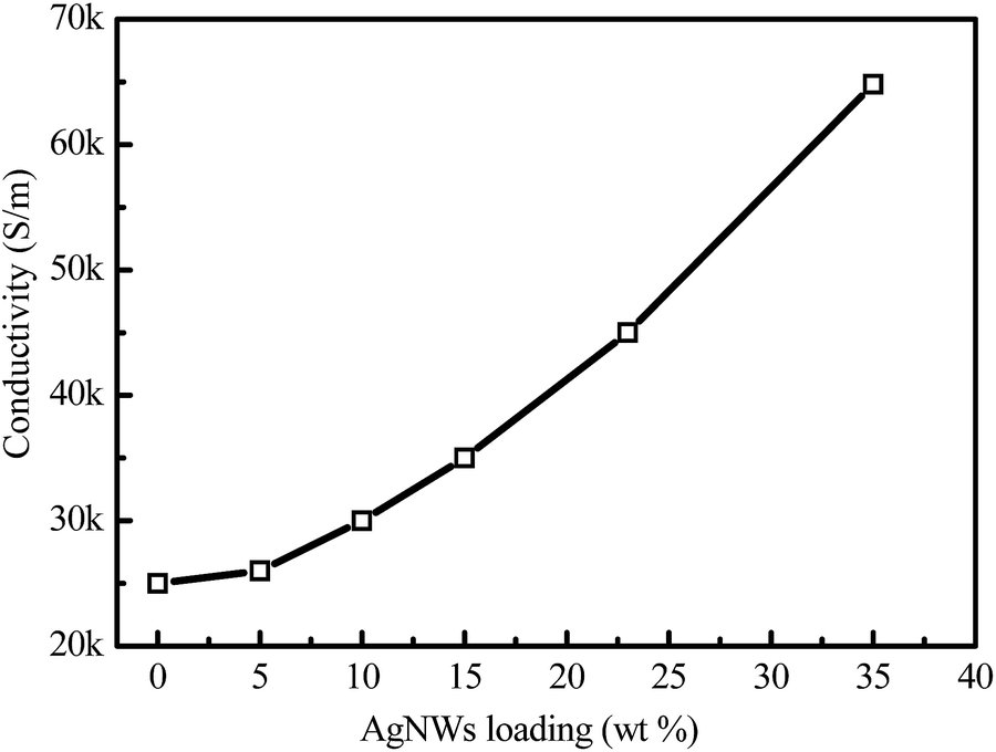 | ||
| Fig. 5 Electrical conductivity of rGO/AgNWs/rGO hybrid thin film. | ||
Finally, we examined the EMI shielding performance of materials using a rectangular holder measurement setup (Vector network analyzer, Agilent E5701C). The EMI shielding effectiveness is defined as the logarithmic ratio of the incident (Pi) to transmitted (Pt) strengths of electromagnetic radiation usually expressed in the decibel (dB) unit. A greater dB level of the EMI SE corresponds to smaller energy transmission through the shielding material. For example, a material with a 20 dB EMI SE value can block 99% of incident EM radiation. In EMI shielding theory, when an EM wave is incident on a shielding material, the incident power is divided into reflected, absorbed, and transmitted power and the corresponding power coefficients of absorbance (A), reflectance (R), and transmittance (T) are such that A + R + T = 1. In a vector network analyzer, we measured the scattering parameters S11 (or S22) and S21 (or S12) to calculate the reflectance and transmittance power coefficient such as R = |S11|2 and T = |S21|2, and the absorbance can be indirectly derived from A = 1 − R − T. The shielding effectiveness could be expressed by the equations:25–27
|
SER = −10log10(1 − R)
| (1) |
|
SEA = −10log10[T/(1 − R)]
| (2) |
| SET = SEA + SER | (3) |
Fig. 6a shows the variation of the total EMI SE for the rGO/AgNWs/rGO sandwich thin films at the X-band (8.4 to 12 GHz) frequency range. At 10 wt% AgNW content, the film shows an efficient enhancement of 24 dB for the shielding efficiency in comparison with the pristine rGO film (∼17 dB) at the same thickness. The shielding effectiveness increases with an increase in the AgNW loading; the total EMI SET value reaches up to ∼38 dB at 35 wt% AgNW loading. We know that EMI shielding mainly depends on the electrical conductivity of the sample. Thus, the enhanced EMI shielding with the AgNW content is attributed to the increased electrical conductivity of the composite film. Furthermore, to clarify the shielding mechanism, the absorption (SEA) and reflection (SER) shielding effectiveness along with the total EMI SE are plotted in Fig. 6b at a frequency of 9 GHz with the AgNW concentration. It is worth noting that the contribution of absorption to the total EMI SE is much greater than that of reflection for all concentrations of the AgNWs. These results suggest that the rGO/AgNWs/rGO hybrid thin films have both reflective and absorptive characters to electromagnetic radiation with absorption as the dominant shielding efficiency.
 | ||
| Fig. 6 (a) Total EMI shielding effectiveness of the hybrid thin film, and (b) SETotal, SEA and SER shielding effectiveness at 9 GHz as a function of the AgNW concentration. | ||
4. Conclusions
In summary, we fabricated a mechanically flexible conductive film composed of graphene and silver nanowires with an improved electrical conductivity presenting an excellent performance of EMI shielding. Graphene sheets were restacked tightly to the silver nanowires, leading to a high electrical conductivity comparable to that of pristine rGO paper. The hybrid sandwich films revealed an excellent EMI SE value of ∼38 dB at a AgNWs content of 35 wt%. We believe that such a simple and effective fabrication procedure will provide a new synthesis pathway for various multifunctional graphene hybrid composite thin films.Acknowledgements
This work was supported by Fundamental R&D Program for Core Technology of Materials, and Industrial Strategic Technology Development Program funded by the Ministry of Trade, Industry and Energy, Republic of Korea, and partially supported by Nano Materials Technology Development Program through the National Research Foundation of Korea (NRF) funded by the Ministry of Science, ICT and Future Planning, Republic of Korea, and by the Korea Institute of Science and Technology. PK also acknowledges the financial support from Department of Science and Technology, India under DST INSPIRE Faculty Award.References
- N. Li, Y. Huang, F. Du, X. He, X. Lin, H. Gao, Y. Ma, F. Li, Y. Chen and P. C. Eklund, Nano Lett., 2006, 6, 1141–1145 CrossRef CAS PubMed.
- D. D. L. Chung, Carbon, 2001, 39, 279–285 CrossRef CAS.
- Z. Chen, C. Xu, C. Ma, W. Ren and H.-M. Cheng, Adv. Mater., 2013, 25, 1296–1300 CrossRef CAS PubMed.
- F. Shahzad, P. Kumar, S. Yu, S. Lee, Y.-H. Kim, S. M. Hong and C. M. Koo, J. Mater. Chem. C, 2015, 3, 9802–9810 RSC.
- F. Shahzad, S. Yu, P. Kumar, J.-W. Lee, Y.-H. Kim, S. M. Hong and C. M. Koo, Compos. Struct., 2015, 133, 1267–1275 CrossRef.
- R. C. Hansen and W. T. Pawlewicz, IEEE Trans. Microwave Theory Tech., 1982, 30, 2064–2066 CrossRef.
- B. Shen, W. Zhai and W. Zheng, Adv. Funct. Mater., 2014, 24, 4542–4548 CrossRef CAS.
- B. Wen, M. Cao, M. Lu, W. Cao, H. Shi, J. Liu, X. Wang, H. Jin, X. Fang, W. Wang and J. Yuan, Adv. Mater., 2014, 26, 3484–3489 CrossRef CAS PubMed.
- K. Batrakov, P. Kuzhir, S. Maksimenko, A. Paddubskaya, S. Voronovich, P. Lambin, T. Kaplas and Y. Svirko, Sci. Rep., 2014, 4, 7191 CrossRef CAS PubMed.
- C. Lee, X. Wei, J. W. Kysar and J. Hone, Science, 2008, 321, 385–388 CrossRef CAS PubMed.
- Y. Zhu, S. Murali, W. Cai, X. Li, J. W. Suk, J. R. Potts and R. S. Ruoff, Adv. Mater., 2010, 22, 3906–3924 CrossRef CAS PubMed.
- F. Shahzad, P. Kumar, Y.-H. Kim, S. M. Hong and C. M. Koo, ACS Appl. Mater. Interfaces, 2016, 8, 9361–9369 CAS.
- W.-L. Song, L.-Z. Fan, M.-S. Cao, M.-M. Lu, C.-Y. Wang, J. Wang, T.-T. Chen, Y. Li, Z.-L. Hou, J. Liu and Y.-P. Sun, J. Mater. Chem. C, 2014, 2, 5057–5064 RSC.
- L. Zhang, N. T. Alvarez, M. Zhang, M. Haase, R. Malik, D. Mast and V. Shanov, Carbon, 2015, 82, 353–359 CrossRef CAS.
- P. Kumar, F. Shahzad, S. Yu, S. M. Hong, Y.-H. Kim and C. M. Koo, Carbon, 2015, 94, 494–500 CrossRef CAS.
- W.-L. Song, M.-S. Cao, M.-M. Lu, S. Bi, C.-Y. Wang, J. Liu, J. Yuan and L.-Z. Fan, Carbon, 2014, 66, 67–76 CrossRef CAS.
- T.-W. Lee, S.-E. Lee and Y. G. Jeong, ACS Appl. Mater. Interfaces, 2016, 8, 13123–13132 CAS.
- J. Ma, M. Zhan and K. Wang, ACS Appl. Mater. Interfaces, 2015, 7, 563–576 CAS.
- M. Hu, J. Gao, Y. Dong, K. Li, G. Shan, S. Yang and R. K.-Y. Li, Langmuir, 2012, 28, 7101–7106 CrossRef CAS PubMed.
- P. Kumar, U. N. Maiti, K. E. Lee and S. O. Kim, Carbon, 2014, 80, 453–461 CrossRef CAS.
- P. Kumar, S. Yu, F. Shahzad, S. M. Hong, Y.-H. Kim and C. M. Koo, Carbon, 2016, 101, 120–128 CrossRef CAS.
- S. Pei, J. Zhao, J. Du, W. Ren and H.-M. Cheng, Carbon, 2010, 48, 4466–4474 CrossRef CAS.
- M. A. Pimenta, G. Dresselhaus, M. S. Dresselhaus, L. G. Cancado, A. Jorio and R. Saito, Phys. Chem. Chem. Phys., 2007, 9, 1276–1290 RSC.
- D. R. Dreyer, S. Park, C. W. Bielawski and R. S. Ruoff, Chem. Soc. Rev., 2010, 39, 228–240 RSC.
- Z. Chen, C. Xu, C. Ma, W. Ren and H.-M. Cheng, Adv. Mater., 2013, 25, 1296–1300 CrossRef CAS PubMed.
- H.-B. Zhang, Q. Yan, W.-G. Zheng, Z. He and Z.-Z. Yu, ACS Appl. Mater. Interfaces, 2011, 3, 918–924 CAS.
- V. Eswaraiah, V. Sankaranarayanan and S. Ramaprabhu, Macromol. Mater. Eng., 2011, 296, 894–898 CrossRef CAS.
| This journal is © The Royal Society of Chemistry 2016 |