
Identification of marcasite in pyrite FeS2 thin films and the films' carrier transport characteristics†
Juran Kima,
Gee Yeong Kima,
Hankyoul Moona,
Seokhyun Yoona,
Il Wan Seob,
Yunsang Leeb,
Dong Gwon Mooncd,
SeJin Ahnc and
William Jo*a
aDepartment of Physics, Ewha Womans University, Seoul, 03760, Korea. E-mail: wmjo@ewha.ac.kr; Fax: +82 2 3277 2372; Tel: +82 2 3277 4066
bDepartment of Physics, Soongsil University, Seoul, 06978, Korea
cPhotovoltaic Laboratory, Korea Institute of Energy Research, Daejeon, 34129, Korea
dDepartment of Materials Science and Engineering, Yonsei University, Seoul 03722, Korea
First published on 22nd August 2016
Abstract
In this study, we characterized FeS2 thin films grown by the non-vacuum spin-coating method. We annealed the samples under a sulfur atmosphere at different sulfurization temperatures. The phase transformation from marcasite-containing pyrite to pure pyrite occurs between 350 and 400 °C. The structural phase formation on the films depends on the sulfurization temperature. It is known that pure pyrite thin films are more suitable for solar cells. FeS2 thin films with and without the marcasite phase were investigated in terms of their local electrical properties and carrier transport by conductive atomic force microscopy and Kelvin probe force microscopy. Interestingly, the pure pyrite thin film shows less conducting behavior than the mixed phase sample because the mixed phase thin film has other residues on the surface. Pure pyrite shows two major work functions at 4.64 and 4.70 eV, and the mixed phase sample has multiple surface potential peaks below 4.63 eV, which is the main pyrite FeS2 work function. Pure-phase pyrite thin films are promising for earth-abundant solar cell applications.
Introduction
Iron pyrite (cubic FeS2) is attracting renewed interest as a promising photovoltaic material because of the suitability of its band gap of ∼0.95 eV for earth-abundant materials and its high light absorption coefficient.1 The optical-absorption coefficient in the visible light region is approximately 105 cm−1,1,2 although it has an indirect band gap. Moreover, manufacture of iron pyrite is easy because of its flexibility and small thickness.3,4 Several kinds of solar cells using iron pyrite have been indeed tried and investigated, such as quantum-dot-sensitized solar cells5 and dye-sensitized solar cells.6 However, research in the mid-1980s and 1990s found a low open-circuit voltage (VOC) of around 0.2 V. Compared with cost-competitive thin-film solar cells like Cu2ZnSnS4 (CZTS) with VOC = ∼0.5 V,7 the VOC of iron pyrite is too low for solar cells. Ennaoui et al. considered this to be the main cause of the low conversion efficiency (∼2%).1 Therefore, it is important to understand the limitations of the open-circuit voltage and determine how to can be improved.Bronold et al. and Guanzhou et al. suggested that intrinsic surface states result in band gap states, pinning the Fermi level.8–10 In addition, defects such as sulfur vacancies,1,11–17 extrinsic point defects,18 and trap states19 deteriorate the performance of iron pyrite solar cells. The low efficiency is also considered to be caused by the phase impurities.20 FeS2 thin films are known to contain the marcasite phase as well as the pyrite phase. The mixed phase of FeS2 can deteriorate its photovoltaic performance. Although several researchers have deposited FeS2 thin films using a sputtering method in high vacuum,21 simple deposition techniques are required for competitive costs and application to wide areas. Many groups have attempted to control phase formation while fabricating FeS2 thin films. Dong et al.22 and other researchers have controlled the reaction temperature,17,23–28 sulfurization time,17,29 and growth time30 for pyrite formation. Moon et al.31 suggested that the phase transformation depends on the sulfurization temperature. Wan et al.15,32 and Thomas et al.20 controlled the sulfur pressure,33 and Wadia et al.34 controlled the solution pH during deposition. The electrical properties of FeS2 have been extensively explored under various growth conditions.22,32,33,35–38 A single pyrite phase is studied because of its low resistivity and carrier concentration.
Here, we used conductive atomic force microscopy (C-AFM) and Kelvin probe force microscopy (KPFM) measurements to investigate the electrical properties, namely, the surface current and potential, of FeS2 layers. We also investigated the phase transformation and morphologic alteration by Raman scattering spectroscopy and scanning electron microscopy (SEM).
Experimental
We prepared iron acetate, monoethanolamine, and ethanol for the precursor solution, and sulfur powder was used for sulfurization. The precursor solution was spin-coated on an indium tin oxide (ITO) substrate or Mo-coated soda-lime glass at 2200 rpm for 20 s. We completed sulfurization in a heat-treatment chamber. We controlled the temperature and pressure in the chamber. We controlled the pressure with the injection of N2 gas. We applied sulfurization temperatures of 350 and 400 °C.31We used a commercial atomic force microscope (AFM) (Nanofocus Inc., n-Tracer, Korea) to characterize the electrical properties of the FeS2 surfaces, using a Pt/Ir-coated tip for C-AFM and KPFM (Nanosensor, PPP-EFM). For the C-AFM measurement, we applied an external bias of 0–1.5 V to the precursor surfaces. At the same time, we obtained morphologic images in contact mode. Using KPFM measurements, we obtained the surface potential in non-contact mode. The natural frequency of the tip was 73 kHz and the scan rate was less than 0.5 Hz. The measurements were performed in N2 atmosphere at room temperature in a glove box, where the oxygen level and humidity were <10 ppm and around 20%, respectively. To investigate the surface and cross-sectional morphology and nanostructure, we performed scanning electron microscopy (SEM, XL30SFEG Phillips Co., The Netherlands, at 10 kV). Temperature-dependent Raman spectra were measured using a closed cycle cryostat and a McPherson 207 spectrometer equipped with a nitrogen-cooled charge-coupled device array detector. The samples were excited with a 488 nm diode laser, which was focused to ∼1 μm diameter spot using a long-working distance microscope objective (×100). To investigate the electronic structures of the FeS2 films, we performed reflectivity and transmission measurements of the films grown on ITO substrates in the spectral range 0.5–6.5 eV. We directly calculated the optical constants, refractive index (n), and extinction coefficient (k) from the measured reflectivity and transmission spectra using the Fresnel equation.
Results and discussion
Fig. S1† shows surface and cross-sectional SEM images of FeS2 sulfurized at 350 and 400 °C. The thickness of the spin-coated FeS2 thin film on the glass is 476 nm. Grains can be observed in the thin films. In the surface SEM image of mixed-phase thin film (Fig. S1(a)†), it is not easy to discern the grains compared to that of pure pyrite thin film (Fig. S1(b)†). Seen in the cross-sectional SEM images (Fig. S1(c) and (d)†), the two samples have similar grain sizes. However, the sample annealed at 400 °C shows well-formed spherical grains and grain boundaries (GBs). Formation of the marcasite phase in the sample sulfurized at 350 °C was caused by the low S reaction level owing to the relatively low sulfurization temperature. In contrast, the 400 °C-sulfurized FeS2 underwent a phase transformation to yield the single pyrite phase.39Fig. 1(a) and (b) show optical microscopic images of the 350 and 400 °C sulfurized samples, respectively. The Y-shaped patterns are chapped area formed during the spin-coating method. In the optical images, there are no significant morphological differences between the two samples. However, the phases of the two samples are different. Although the signal is low, it is possible to see existence of the marcasite phase in the sample sulfurized at 350 °C. We performed micro-Raman scattering measurements changing the temperature from −150 to 300 °C (Fig. 1(c) and (d)). For the sample sulfurized at 350 °C, there is a peak associated with the marcasite phase at every measurement temperature, and the spectra obtained at 50 °C are enlarged in Fig. 1(e). As the temperature increased, no phase transformation was observed (i.e., appearance of a new phonon mode or disappearance of an existing mode) during the measurement, although a red shift of the pyrite (Ag) mode occurred owing to temperature-induced softening. According to Meng et al.,17 when the sulfurization temperature is low (e.g., 200 °C, which is the minimum temperature showing crystalline phases as a result of sulfurization), the amount of S is too small to detect. As the sulfurization temperature increases, the reaction between sulfur and iron increases, and a phase transformation occurs. Moon et al.31 also observed the phase transformation. With increasing sulfurization temperature from 250 to 500 °C, iron oxide starts to change to marcasite FeS2, and then completely transforms to pyrite. However, sulfurization temperatures above 500 °C result in decomposition of pyrite, which is converted to pyrrhotite and S vapor. This can be considered to be more sulfur vacancies being created in the lattice.33 In agreement with previous studies, the Raman scattering spectra in this study also substantiate the effect of changing the sulfurization temperature on formation of different phase of FeS2.
 | ||
| Fig. 1 (a) and (b) Optical images of FeS2 thin film grown at 350 °C and 400 °C, respectively. (c) and (d) Temperature-dependent micro-Raman scattering spectra of FeS2 thin films grown at 350 °C and 400 °C measured over a wide temperature range from 83 to 573 K, respectively. (e) The two Raman spectra measured at 323 K showing the marcasite peak at around 320 cm−1 for the 350 °C sulfurized sample. | ||
Fig. S2† shows the complex optical constants of the marcasite-containing and pure pyrite FeS2 films. According to previous studies, the band gap of marcasite FeS2 is smaller than that of pyrite FeS2, which is in agreement with our finding that the band gap of the 350 °C sulfurized FeS2 thin film with a small fraction of the marcasite phase is slightly smaller than that of the pure pyrite FeS2 film.39
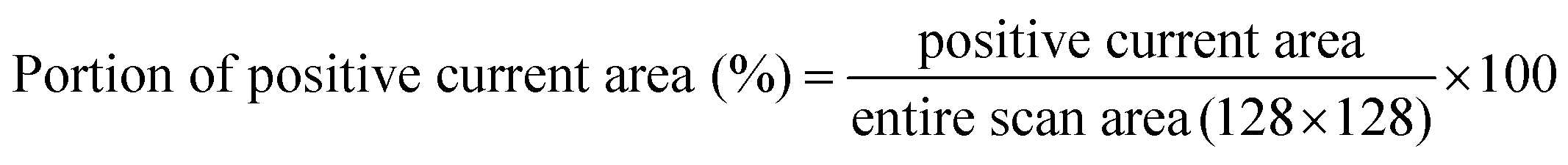
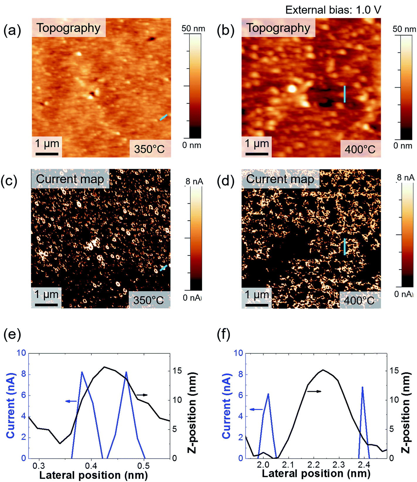
We measured the surface currents of the samples. Fig. 2(a) and (b) show the topologies of the two thin films, and the surface current maps of the samples are shown in Fig. 2(c) and (d). From the line profiles of the results (Fig. 2(e) and (f)), a surface current is formed along the GBs and the marcasite-containing sample has a higher current value. In addition to the current maps and line profiles, further analysis is required in terms of the current development between the two samples. Thus, we calculated the average current and the portion of the positive current area (Fig. 3(a) and (b)):
 | (1) |
 | ||
| Fig. 2 (a) and (b) Topographies of FeS2 thin films grown at 350 and 400 °C, respectively. (c) and (d) Current maps of FeS2 thin film grown at 350 and 400 °C, respectively. Both current maps were obtained under an external bias of 1 V. (e) Line profiles of the current and height of the FeS2 thin film grown at 350 °C and (f) line profiles of the current and height of the FeS2 thin film grown at 400 °C. | ||
 | ||
| Fig. 3 (a) Average current of the FeS2 films. (b) Positive current area of the FeS2 films. (c) I–V curves of the FeS2 films. The I–V curves are the average values of more than five different spots. | ||
Azulay et al. reported that in the dark, positive current is generated near the GBs on light absorber layer surfaces.40 Based on this, we can calculate the portion of the positive current area of the surfaces. Although the average current of the iron pyrite film is lower, the portion of the positive current is much larger than that of the marcasite-containing FeS2 thin film. According to Meng et al.,33 a FeS2 thin film with low phase impurity has low resistivity and high carrier density. In contrast, FeS2 thin film annealed at lower temperatures have higher carrier concentrations because it contains FeS and marcasite phase.22 Because FeS is metal and marcasite has a lower band gap than pyrite, they can cause high current on the film surface. The potential barrier near the GBs decreases as the number of defects decreases.21,22,40 It is possible to understand the construction of structural defects in pyrite as an outcome of formation of marcasite.37 We consider that although it is more conductive, marcasite induces the formation of defects, so it lowers the carrier transportation area on the FeS2 thin film. From these results, we believe that when it is fabricated as a solar cell device, the pure phase FeS2 thin film will perform better than the marcasite-containing FeS2 thin film. Fig. 3(c) shows I–V curves of FeS2 with and without the marcasite phase. We obtained the curves by averaging the data from several points. As shown in Fig. S1,† the sample sulfurized at 350 °C shows relatively ambiguous GB formation. Thus, we suggest that the marcasite phase should be distributed on the surface. The shapes of the curves are similar to the Schottky curve. The Schottky barrier of the 400 °C sulfurized sample is slightly larger than that of the 350 °C sulfurized sample. This can aid in explaining the C-AFM measurements and carrier behavior on the FeS2 surfaces. Furthermore, the carrier barrier slightly differed depending on the location in both samples, so we can expect the existence of secondary phases. The surface current significantly differed depending on the position. The pattern is a chapped area during spin coating, but we can assume that the distribution of the secondary phases is slightly larger in those areas. Therefore, because marcasite is a lower band gap material, it seems to be more conducting.
We also performed KPFM measurements for both samples. The surface topographies are shown in Fig. 4(a) and (b), and the potential maps are shown in Fig. 4(c) and (d). We then calculated the work function of both samples (Fig. 4(e) and (f)):
 | (2) |
 | ||
| Fig. 4 (a) and (b) Topographies of FeS2 thin films grown at 350 and 400 °C, respectively. (c) and (d) Current maps of FeS2 thin films grown at 350 and 400 °C, respectively. (e) Work function of the FeS2 thin film grown at 350 °C, showing several surface potential peaks below 4.63 eV. (f) Work function of the current and height of the FeS2 thin film grown at 400 °C. | ||
We were able to determine that the surface potential differs depending on the location. A positively charged potential develops near the edge of the grains, which means we can apply GB theory to the FeS2 thin films. It is known that potential bending occurs at the GBs of chalcogen-based materials. The origin and bending characteristics are not universal, but they are likely to be because of the distorted lattice and unsaturated chalcogen-bonds near the GBs.21,40,41 A number of studies have investigated the phase and texture in solar cells, such as Cu2ZnSn(S,Se)4![[thin space (1/6-em)]](https://www.rsc.org/images/entities/char_2009.gif) 42–45 and Cu(In,Ga)Se2 solar cells.46–48 Because electron–hole pair recombination is important, development of downward band bending near GBs can be helpful for carrier transport. An electrostatic force is created when GBs act as a main current flow path that is dominated by minority carriers, where electron–hole pair recombination is hindered. Improvement of the phase transition and noticeable GBs formation is observed in Fig. S1.† Moreover, in Fig. 2(e) and (f), the surface current forms to avoid IGs. Thus, the role of the GBs could pertain to FeS2 thin films as a light-absorber in solar cells. Although recognizing GBs with AFM measurements is not easy because of their very small grains and small surface roughness, we were able to see topographical improvement (Fig. S1†) and an increase of the surface potential (Fig. 4).
42–45 and Cu(In,Ga)Se2 solar cells.46–48 Because electron–hole pair recombination is important, development of downward band bending near GBs can be helpful for carrier transport. An electrostatic force is created when GBs act as a main current flow path that is dominated by minority carriers, where electron–hole pair recombination is hindered. Improvement of the phase transition and noticeable GBs formation is observed in Fig. S1.† Moreover, in Fig. 2(e) and (f), the surface current forms to avoid IGs. Thus, the role of the GBs could pertain to FeS2 thin films as a light-absorber in solar cells. Although recognizing GBs with AFM measurements is not easy because of their very small grains and small surface roughness, we were able to see topographical improvement (Fig. S1†) and an increase of the surface potential (Fig. 4).
Conclusion
We identified the phases of FeS2 thin films grown at 350 and 400 °C. Sulfurization at the higher temperature improves thin film growth and the pure pyrite phase forms. FeS2 sulfurized at 350 °C shows the marcasite–pyrite mixed phase. The pyrite FeS2 thin film has well-formed grains and current develops along the GBs. However, the marcasite–pyrite mixed phase FeS2 thin film has vague GBs and grain formation is poor. Surface current and a positively charged potential develops near the GBs. Thus, we expect that the pyrite FeS2 thin film has a negligible effect on the GBs, like chalcogenide thin film solar cells. In particular, from statistics, the I–V curves, and optical investigation, we conclude that the existence of marcasite leads to higher conductivity. However, the pure pyrite sample has a larger current area. Furthermore, because the pyrite FeS2 thin film has a single work function peak (at around 4.63 eV), we verified uniform phase formation at the higher sulfurization temperature. Therefore, we expect that FeS2 with the pure pyrite phase will perform better as a light absorber in solar cells.Acknowledgements
JK, GYK and WJ at Ewha acknowledge the support by the New & Renewable Energy of the Korea Institute of Energy Technology Evaluation and Planning (KETEP) grant funded by the Korea government, Ministry of Trade, Industry, and Energy (No. 20123010010130). DGM and SJA at KIER acknowledge the support by the New & Renewable Energy Core Technology Program of the Korea Institute of Energy Technology Evaluation and Planning (KETEP) funded by the Ministry of Trade, Industry, Energy of Korea (No. 20143030011950). HM and SY at Ewha acknowledge the support by the National Research Foundation of Korea (NRF) with grants funded by the Korea government (MSIP) (2013 R1A1A2007951 and No. 2015001948).References
- A. Ennaoui, S. Fiechter, C. Pettenkofer, N. Alonso-Vante, K. Büker, M. Bronold, C. Höpfner and H. Tributsch, Sol. Energy Mater. Sol. Cells, 1993, 29, 289 CrossRef CAS.
- L. Yu, S. Lany, R. Kykyneshi, V. Jieratum, R. Ravichandran, B. Pelatt, E. Altschul, H. A. S. Platt, J. F. Wager, D. A. Keszler and A. Zunger, Adv. Energy Mater., 2011, 1, 748 CrossRef CAS.
- A. Ennaoui, S. Fiechter, H. Goslowsky and H. Trobutsch, J. Electrochem. Soc., 1985, 132, 1579 CrossRef CAS.
- H. Xian, J. Zhu, X. Liang and H. He, RSC Adv., 2016, 6, 31988 RSC.
- M. Wang, H. Qin, Y. Fang, J. Liu and L. Meng, RSC Adv., 2012, 5, 105324 RSC.
- J. Guo, S. Liang, Y. Shi, C. Hao, X. Wang and T. Ma, RSC Adv., 2015, 5, 72553 RSC.
- W. Wang, M. T. Winkler, O. Gunawan, T. Gokmen, T. K. Todorov, Y. Zhu and D. B. Mitzi, Adv. Energy Mater., 2014, 4, 1301465 CrossRef.
- M. Bronold, Y. Tomm and W. Jaegermann, Surf. Sci., 1994, 314, L931 CrossRef CAS.
- M. Bronold, K. Büker, S. Kubala, C. Pettenkofer and H. Tributsch, Phys. Status Solidi A, 1993, 135, 231 CrossRef CAS.
- Q. Guanzhou, X. Qi and H. Yuehua, Comput. Mater. Sci., 2004, 29, 89 CrossRef.
- I. J. Ferrer and C. Sánchez, J. Appl. Phys., 1991, 70, 2641 CrossRef CAS.
- M. Birkholz, S. Fiechter, A. Hartmann and H. Tributsch, Phys. Rev. B: Condens. Matter Mater. Phys., 1991, 43, 11926 CrossRef CAS.
- M. Bronold, C. Pettenkofer and W. Jaegermann, J. Appl. Phys., 1994, 76, 5800 CrossRef CAS.
- G. U. von Oertzen, W. M. Skinner and H. W. Nesbitt, Phys. Rev. B: Condens. Matter Mater. Phys., 2005, 72, 235427 CrossRef.
- D. Wan, Y. Wang, B. Wang, C. Ma, H. Sun and L. Wei, J. Cryst. Growth, 2003, 253, 230 CrossRef CAS.
- L. Meng, J. P. Tu and M. S. Liu, Mater. Lett., 1999, 38, 103 CrossRef CAS.
- L. Meng and M. S. Liu, Mater. Sci. Eng., B, 1999, 60, 168 CrossRef.
- A. M. Abd El Halim, S. Fiechter and H. Tributsch, Electrochim. Acta, 2002, 47, 2615 CrossRef CAS.
- B. Ouertani, J. Ouerfelli, M. Saadoun, B. Bessaïs, H. Ezzaouia and J. C. Bernède, Mater. Charact., 2005, 54, 431 CrossRef CAS.
- B. Thomas, T. Cibik, C. Höpfner, K. Diesner, G. Ehlers, S. Fiechter and K. Ellmer, J. Mater. Sci.: Mater. Electron., 1998, 9, 61 CrossRef CAS.
- D. Lichtenberger, K. Ellmer, R. Schieck and S. Fiechter, Appl. Surf. Sci., 1993, 70/71, 583 CrossRef.
- Y. Z. Dong, Y. F. Zheng, H. Duan, Y. F. Sun and Y. H. Chen, Mater. Lett., 2005, 59, 2398 CrossRef CAS.
- R. J. Soukup, P. Prabukanthan, N. J. Ianno, A. Sarkar, C. A. Kamler and D. G. Sekora, J. Vac. Sci. Technol., A, 2011, 29, 011001 Search PubMed.
- N. Berry, M. Cheng, C. L. Perkins, M. Limpinsel, J. C. Hemminger and M. Law, Adv. Energy Mater., 2012, 2, 1124 CrossRef CAS.
- D. M. Schleich and H. S. W. Chang, J. Cryst. Growth, 1991, 112, 737 CrossRef CAS.
- A. Kirkeminde, B. A. Ruzicka, R. Wang, S. Puna, H. Zhao and S. Ren, ACS Appl. Mater. Interfaces, 2012, 4, 1174 CAS.
- G. Willeke, R. Dasbach, B. Sailer and E. Bucher, Thin Solid Films, 1992, 213, 271 CrossRef CAS.
- T. R. Rana, D. B. Khadka and J. H. Kim, Mater. Sci. Semicond. Process., 2015, 40, 325 CrossRef CAS.
- J. Puthussery, S. Seefeld, N. Berry, M. Gibbs and M. Law, J. Am. Chem. Soc., 2011, 133, 716 CrossRef CAS PubMed.
- H. T. Kim, T. P. N. Nguyen, C. D. Kim and C. Park, Mater. Chem. Phys., 2014, 148, 1095 CrossRef CAS.
- D. G. Moon, A. Cho, J. H. Park, S. H. Ahn, H. S. Kwon, Y. S. Cho and S. J. Ahn, J. Mater. Chem. A, 2014, 2, 17779 CAS.
- D. Wan, B. Wang, Y. Wang, H. Sun, R. Zhang and L. Wei, J. Cryst. Growth, 2003, 257, 286 CrossRef CAS.
- L. Meng, Y. H. Liu and W. Huang, Mater. Sci. Eng., B, 2002, 90, 84 CrossRef.
- C. Wadia, Y. Wu, S. Gul, S. K. Volkman, J. Guo and A. P. Alivisatos, Chem. Mater., 2009, 21, 2568 CrossRef CAS.
- L. Meng, Y. H. Liu and L. Tian, Mater. Res. Bull., 2003, 38, 941 CrossRef CAS.
- A. Yamamoto, M. Nakamura, A. Seki, E. L. Li, A. Hashimoto and S. Nakamura, Sol. Energy Mater. Sol. Cells, 2003, 75, 451 CrossRef CAS.
- S. Seefeld, M. Limpinsel, Y. Liu, N. Farhi, A. Weber, Y. Zhang, N. Berry, Y. J. Kwon, C. L. Perkins, J. C. Hemminger, R. Wu and M. Law, J. Am. Chem. Soc., 2013, 135, 4412 CrossRef CAS PubMed.
- J. Y. W. Seto, J. Appl. Phys., 1975, 46, 5247 CrossRef CAS.
- I. Dódony, M. Pósfai and P. R. Buseck, Am. Mineral., 1996, 81, 119 Search PubMed.
- D. Azulay, O. Millo, I. Balberg, H. W. Schock, I. Visoly-Fisher and D. Cahen, Sol. Energy Mater. Sol. Cells, 2007, 91, 85 CrossRef CAS.
- J. Bruneaux, H. Cachet, M. Froment and A. Messad, Thin Solid Films, 1991, 197, 129 CrossRef CAS.
- A. R. Jeong, W. Jo, S. Jung, J. Gwak and J. H. Yun, Appl. Phys. Lett., 2011, 99, 082103 CrossRef.
- G. Y. Kim, A. R. Jeong, J. R. Kim, W. Jo, D.-H. Son, D.-H. Kim and J.-K. Kang, Sol. Energy Mater. Sol. Cells, 2014, 127, 129 CrossRef CAS.
- J. B. Li, V. Chawla and B. M. Clemens, Adv. Mater., 2012, 24, 720 CrossRef CAS PubMed.
- G. Y. Kim, J. R. Kim, W. Jo, D.-H. Son, D.-H. Kim and J.-K. Kang, Nanoscale Res. Lett., 2014, 9, 10 CrossRef PubMed.
- M. Rusu, Th. Glatzel, A. Neisser, C. A. Kaufmann, S. Sadewasser and M. C. Lux-Steiner, Appl. Phys. Lett., 2006, 88, 143510 CrossRef.
- D. Fuertes Marrón, A. Meeder, S. Sadewasser, R. Würz, C. A. Kaufmann, T. Glatzel, T. Schedel-Niedrig and M. C. Lux-Steiner, J. Appl. Phys., 2005, 97, 094915 CrossRef.
- S. Sadewasser, Phys. Status Solidi A, 2006, 203, 2571 CrossRef CAS.
Footnote |
| † Electronic supplementary information (ESI) available. See DOI: 10.1039/c6ra18581a |
| This journal is © The Royal Society of Chemistry 2016 |