DOI:
10.1039/C6RA18433B
(Paper)
RSC Adv., 2016,
6, 114566-114571
The large response current of a vacuum pressure sensor based on a vertically-aligned ZnO nanowires array
Received
20th July 2016
, Accepted 30th September 2016
First published on 14th November 2016
Abstract
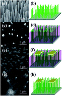
A vertically-aligned ZnO nanowires (VA-ZnO-NWs) array was prepared via chemical vapor deposition, which was used to fabricate a vacuum pressure sensor and its sensitive characteristics were measured using a semiconductor parameter tester. The response currents are larger than those of the previous sensors based on ZnO nanobelts (NBs) film, ZnO single NW and p-ZnO nanowires. There is a linear relationship in the resistance–vacuum pressure curve of the logarithmic coordinate system. The measurement of the vacuum pressure is in the range of 10−5 to 103 mbar and the power consumption is in the range of 102 to 103 μW, which is wider and much lower, respectively, compared with the traditional vacuum pressure sensors. The current–time curve of the vacuum pressure variation was used to study the response speed and repeatability. The sensitive mechanism is discussed using oxygen chemisorption and the unique NWs array structure to understand the large response current and high sensitivity of the VA-ZnO-NWs array sensor. The adsorbed oxygen on the large surface area of the ZnO NWs can form an electron depletion layer on the surface, and the unique NWs array structure with large surface-to-volume ratio provides abundant carrier channels for electronic transport.
1. Introduction
In recent years, one-dimensional nanostructured materials, such as nanowires (NWs), nanobelts (NBs) and nanotubes have been successfully synthesized and have attracted much attention for a wide range of potential applications, including applications in chemistry, physics, electronics, optics, materials science, biomedical science and nanodevices.1 Significant progress has been made in the application of ZnO nanostructures to fabricate various electronic, optoelectronic and sensor devices, and they include ultraviolet-light sensors,2 solar cells,3 nanogenerators,4,5 energy converters,6 and gas sensors.7 Effective applications in industry for vacuum pressure sensing schemes are found using surface-micromachining technology for a micro-hotplate thermal vacuum sensor8 and a self-heated microbridge for a Pirani pressure sensor;9 however, they are unsuitable for an integrated circuit due to their large size.10 It is very interesting and promising to employ field emission (FE) devices,11 micro-electro-mechanical systems (MEMS) and micro-opto-electro-mechanical systems (MOEMS) to minimize the size of vacuum pressure sensors.12,13 However, the manufacturing processes of vacuum pressure sensors are generally complex and the high cost of signal detecting/amplifying electronics needs to be considered before their practical applications. These drawbacks make MEMS, MOEMS and FE devices difficult to commercialize as practical vacuum pressure sensors.14 Generally, one-dimensional semiconductor nanomaterials have a large length-to-diameter aspect ratio and high surface-to-volume ratio in order to provide a large current/conductivity response in electronic, optoelectronic and sensor devices, such as the photoconductive semiconductor switch comprised of a ZnS-NBs film,15 a room temperature oxygen sensor comprised of ZnO NWs,16 a battery-less chemical detector based on an vertically-aligned ZnO nanowires (VA-ZnO-NWs) array5 and a room-temperature self-powered ethanol sensor based on an Pd/ZnO NWs array.17 The vacuum pressure sensors based on ZnO-NBs film, ZnO single NW and p-ZnO nanowires have been reported recently;14,18,19 however, their extremely weak current signals make them difficult to be applied in practical measurements. We naturally associate whether the response current of a vacuum pressure sensor can be improved by employing a VA-ZnO-NWs array that possesses more carrier channels in the limited space.
In this study, we designed a vacuum pressure sensor based on a VA-ZnO-NWs array in order to improve the sensing performance through increasing the response current and the current–voltage (I–V) characteristics were measured under the different vacuum pressures to establish the sensitivity–pressure (S–P), resistance–pressure (R–P) and power consumption–pressure (P–P) curves. The pressure sensitivity, measurement range and power consumption of the vacuum pressure sensor were compared with previous vacuum pressure sensors to identify its potential application field.8–10,14,18,19 The current–time (I–T) curves of the VA-ZnO-NWs array and ZnO-NBs film sensors were measured at two cycles of the vacuum pressure variation to investigate the sensor's repeatability. The sensitive mechanism is discussed from the oxygen chemisorption and surface-to-volume ratio to understand the large response current of the VA-ZnO-NWs array sensor. This research may provide useful guidelines for the practical application of one-dimensional array semiconductor materials in designing high performance gas sensors.
2. Experimental
2.1 Synthesis and characterization of the VA-ZnO-NWs array
The VA-ZnO-NWs array was grown on a 3 mm × 3 mm a-plane sapphire substrate using the CVD method and the growth temperature and time were 910 °C and 5 min, respectively.5 The surface morphologies of the as-synthesized nanomaterials were recorded by field emission scanning electron microscopy (FE-SEM, JEOL, JSM-6700F, Japan). Phase identification and crystalline orientation were investigated by XRD (XRD, Rigaku, D/Max 2400, Japan) with Cu-Kα radiation (λ = 0.15406 nm) in the range of 20–80° at room temperature.
2.2 Fabrication of the VA-ZnO-NWs array sensor
The fabrication process of the vacuum pressure sensor based on a VA-ZnO-NWs array was traced by FE-SEM images. The original VA-ZnO-NWs array is given in Fig. 1(a) and it is schematized as Fig. 1(b). The abovementioned observations show that the diameter and length of the NWs are in the ranges of 80–120 nm and 3–5 μm, respectively and the areal density is about 20 μm−2. Polymethylmethacrylate (PMMA) was filled in the VA-ZnO-NWs array and it was cured at room temperature for 24 h. An oxygen plasma etching process was employed to preferentially etch away the PMMA and expose the VA-ZnO-NWs array tips. This process was carried out using a reactive ion etching system with an operation power of 300 W, an oxygen flow rate of 90 sccm, and etching time of 3–5 min. As shown in Fig. 1(c) and (d), the tips of VA-ZnO-NWs array are on the top and PMMA is filled below the tips. In Fig. 1(e), using a mask cover on the array, two Au electrodes with the thickness of 200 nm were deposited on the exposed tip ends of the VA-ZnO-NWs array via e-beam evaporation, and the Au film was attached on the tips of the VA-ZnO-NWs array, as shown in Fig. 1(f). PMMA was removed by dipping into tetrachloroethane, and the VA-ZnO-NWs array was further dried in a vacuum oven at 100 °C. The Au electrode film remained at the top of the VA-ZnO-NWs array after removing PMMA, whereas the VA-ZnO-NWs array was exposed to air beside the Au film, as shown in Fig. 1(g). There is the presence of a thin underlying ZnO film on top of the sapphire substrate,5 and Fig. 1(h) shows that the vacuum pressure sensor based on the VA-ZnO-NWs array comprised of the Au electrodes, VA-ZnO-NWs array, ZnO film, and sapphire substrate.
 |
| Fig. 1 FE-SEM images and schematic diagrams for the VA-ZnO-NWs array (a) and (b), the VA-ZnO-NWs array after filling with PMMA and etching via oxygen plasma etching (c) and (d), the VA-ZnO-NWs array after depositing the Au electrode (e) and (f), and the VA-ZnO-NWs array sensor after removing PMMA (g) and (h). | |
2.3 Characterization using the VA-ZnO-NWs array sensor
The vacuum pressure sensor based on VA-ZnO-NWs array was placed in a vacuum chamber, and the pressure in the vacuum chamber was controlled using the display on the vacuum pressure gauge via the molecular pump (Varian, TV-2KG, USA). Two probes, which could be precisely moved through the probe controller as similar as a micrometer caliper, were connected to the Au electrodes considering the standard integrated circuit drive power,6 and the I–V curves were measured from 0 to 10 V under different vacuum pressures by combining with the semiconductor parameter tester (Agilent, 4156C, USA) and probe station (Lakeshore, TTP4, USA). The vacuum pressure in the vacuum chamber was at a standard atmospheric pressure, the same as the atmospheric environment, which can be adjusted to achieve a 50% relative humidity using a dehumidifier. After the pressure was lowered in the vacuum chamber via the molecular pump at room temperature (25 °C), the I–V characteristics were obtained to establish the S–P, R–P and P–P curves. By comparing with the previous reports, the I–T curves obtained for the vacuum pressure sensors based on the VA-ZnO-NWs array and ZnO NBs film were measured at 10 V using two cycles of the vacuum pressure variation in order to investigate the sensor's repeatability. The vacuum pressure sensors based on the ZnO NBs film were fabricated by assembling a ZnO nanobelt film on the interdigital electrodes.18 In a certain cycle of 540 s, after being kept at standard atmospheric pressure for 60 s, the molecular pump was turned on to decrease the vacuum pressure to 5 × 10⁻² mbar for 180 s and then turned off to maintain the stable vacuum pressure for 100 s. Then, the valve was opened for 200 s.
3. Results and discussion
3.1 XRD characterization
Fig. 2 shows the XRD pattern of the VA-ZnO-NWs array grown on the a-plane sapphire substrate. Herein, the ZnO phase was comprised of a hexagonal wurtzite structure with lattice constants a = 0.325 nm and c = 0.521 nm, which are consistent with the standard values (JCPDS no. 36-1451).20 The diffraction peak was indexed as (002) indicating that the as-grown ZnO NWs were preferentially oriented along the c-axis direction and exhibit a remarkable preferred orientation with high quality.21
 |
| Fig. 2 The XRD pattern of the VA-ZnO-NWs array. | |
3.2 I–V characteristics
As shown in Fig. 3, the I–V curves of the vacuum pressure sensor based on the VA-ZnO-NWs array were measured to investigate its conductivity. The response current increases linearly with the measurement voltage, which indicates that the contacts between the electrodes and nanomaterials are stable ohmic contacts.22 The response currents significantly increase with a decrease in the vacuum pressure at 10 V and they are 18.4, 41.5, 57.8, 107 and 259 μA under vacuum pressures of 1.0 × 10³, 1.1 × 10⁻¹, 2.0 × 10⁻², 8.0 × 10⁻⁴ and 5.0 × 10⁻⁵ mbar, respectively. The lower the vacuum pressure, the stronger the response current is. At the measurement voltage of 10 V, the response currents of the sensor based on the VA-ZnO-NWs array at a vacuum pressure of 10−5 to 103 mbar were about three orders of magnitude higher than those based on the ZnO-NBs film.18 The NWs array structure leads to a giant enhancement of the response current. Evidently, the response current of the vacuum pressure sensor based on the VA-ZnO-NWs array was much larger than that of the sensor based on ZnO nanobelts under the same vacuum pressure. The VA-ZnO-NWs array sensor was sensitive over the range of 10−5 to 103 mbar and it is at least one order of magnitude wider than that of the previous reported sensors, such as the micro-hotplate thermal vacuum sensor (10−2 to 103 mbar), Pirani pressure sensor (0.2 to 200 mbar), FE device (10−9 to 10−4 mbar), and MEMS (520 to 1040 mbar).8–12 The wide measurement range can provide convenient service for industrial or experimental measurements operated over a broad vacuum pressure variation range. Furthermore, NW array sensors and transistors are easy to implant into a sensing circuit,12 and they can be assembled to enable on-chip sensing and signal transistor amplification.23
 |
| Fig. 3 The I–V characteristics of the VA-ZnO-NWs array sensor under the different vacuum pressures. | |
3.3 S–P relationship of the VA-ZnO-NWs array sensor
Usually, the sensitivity S = (Iv − Ia)/Ia is introduced to estimate a sensor's sensibility,18 where Ia and Iv are the response currents under standard atmosphere pressure and vacuum pressure, respectively. From Fig. 3, the sensitivities S were calculated as 1.26, 2.19, 4.82 and 13.08 under the vacuum pressures of 1.1 × 10⁻¹, 2.0 × 10⁻², 8.0 × 10⁻⁴ and 5.0 × 10⁻⁵ mbar, respectively and the S–P relationship of the vacuum pressure sensor based on the VA-ZnO-NWs array was summarized in Fig. 4. The sensitivity of the VA-ZnO-NWs array sensor was 4.82 at 8.0 × 10⁻⁴ mbar and was higher than 4.29 at 8.2 × 10⁻⁴ mbar found for the ZnO-NBs film sensor.18 The high sensitivity shows that the response current changes significantly with the vacuum pressure and it indicates that the vacuum pressure sensor based on the VA-ZnO-NWs array has a potential use in developing a new class of vacuum pressure sensor.
 |
| Fig. 4 The S–P relationship of the vacuum pressure sensor based on the VA-ZnO-NWs array and ZnO-NBs film.18 | |
3.4 R–P relationship of VA-ZnO-NWs array sensor
Resistance R can be obtained using the ohmic law from Fig. 3, and the R–P curve in logarithmic coordinate system is extracted as shown in Fig. 5. The two types of vacuum pressure sensors based on the VA-ZnO-NWs array and ZnO-NBs film18 were compared in order to identify the effect of the nanostructure on the resistance. Herein, there are evident linear relationships between the resistance and vacuum pressure for both sensors. The resistances are in the range of several dozen to several hundred kΩ at 10−5 to 103 mbar for the former, and they are three orders of magnitude lower than those of the latter.
 |
| Fig. 5 The R–P curves obtained for the vacuum pressure sensors based on the VA-ZnO-NWs array and ZnO-NBs film.18 | |
Generally, the nanodevice resistance contains the inherent resistance affected by the oxygen chemisorption and the contact resistance due to the contact of the nanomaterials.24,25 For inherent resistance, the high density of the VA-ZnO-NWs array means a large quantity of conductive NWs connecting the two electrodes, while there are about several hundreds of ZnO NBs on the interdigital electrodes.18 Because the unique NWs array can provide abundant carrier channels for electronic transport,26 there is lower resistance in the VA-ZnO-NWs array than in other nanostructures. In addition, the electrical resistance of one-dimensional nanomaterials is given by27–29
|
 | (1) |
where
n0 is the original carrier concentration,
e is the electronic charge,
μ is the mobility of electrons,
L and
S are the length and cross-sectional area of NW, respectively. The length of the VA-ZnO-NWs array, namely the distance between Au electrode and sapphire substrate, was estimated to be 3–5 μm; however, the length of interdigital electrode separation is only regarded as 45 μm for the ZnO-NBs.
18 The low length can increase the conductance and decrease the inherent resistance, so that the inherent resistance of the VA-ZnO-NWs array should be much lower than that of the ZnO-NBs film. Unlike ZnO-NBs free dispersal on the interdigital electrodes,
18 the tips of the VA-ZnO-NWs array are completely wreathed by the Au electrodes deposited by e-beam evaporation, as shown in
Fig. 2(g), therefore the contact resistance of the VA-ZnO-NWs array should be much lower than that of the ZnO-NBs film. In other words, the total resistance of the VA-ZnO-NWs array under the different vacuum pressures was much lower than that of the ZnO-NBs film, as shown in
Fig. 5. The sensors based on the ZnO-NBs film,
18 single ZnO NW
13 and
p-ZnO
14 are not practical due to the nanoscale current output or giga-ohm electrical resistance, which is bottleneck for large-scale industrial applications. The response current of the VA-ZnO-NWs array sensor is enhanced by about three orders of magnitude compared with the ZnO-NBs film sensor, and the electrical resistance is in the range of several tens to several hundred kΩ, which makes its measurement very simple and easy. Evidently, the total resistance linearly increases with the logarithmical pressure for both sensors and it indicates that the vacuum pressure can be sensed through the
R–
P curve in the applications of thin film deposition, biomedical experiments or industrial process control.
3.5 P–P relationship of the VA-ZnO-NWs array sensor
The P–P curves in a logarithmic coordinate system were extracted from Fig. 3 and are given in Fig. 6. Herein, the power consumption at 10 V was in the range of 102 to 103 μW for the VA-ZnO-NWs array sensor at a pressure range of 10−5 to 103 mbar and it was about three orders of magnitude higher than that of the ZnO-NBs film sensor; however, it was much lower than those of the traditional vacuum pressure sensor, such as a micro-hotplate thermal vacuum sensor (9 mW), Pirani pressure sensor (11.1–91 mW) and FE device (0.22 W).8–11 The relatively low power consumption indicates that the VA-ZnO-NWs array sensor can bring lower energy loss, less heat and prolong the device's life.30
 |
| Fig. 6 The P–P curves obtained for the vacuum pressure sensors based on the VA-ZnO-NWs array and ZnO-NBs film.18 | |
3.6 I–T characteristics
The I–T curves were measured over two cycles of the vacuum pressure variation in order to investigate the repeatability, response and recovery speed, and the results are given in Fig. 7 for both the VA-ZnO-NWs array and ZnO-NBs film sensors. There are approximately two same current fluctuations and this indicates that the signal was repeatable. The response currents are steady at 18 μA and 8.7 nA for the sensors based on the VA-ZnO-NWs array and ZnO-NBs film after opening the valve and turning off the molecular pump within the range of 0–60 s for “1” state. The response currents synchronously increase with decreasing vacuum pressure from standard atmospheric pressure to 5 × 10⁻² mbar within the range of 60–240 s for “2” state after opening the valve and turning on the molecular pump because the current response was faster than the vacuum pressure variation measured using the vacuum gauge. When both the valve and molecular pump were turned off, the response currents were steady at 47.6 μA and 22 nA within the range of 240–340 s for “3” state. The response and recovery speed was defined as v = ΔI/Δt where Δt is the response time or the recovery time of the sensors. Therefore, the νres values for the two sensors were about 0.18 μA s−1 and 0.08 nA s−1, respectively. After opening the valve and turning off the molecular pump to fill air for 340 s, the vacuum pressure increases to the standard atmospheric pressure within 20 s. Moreover, the response currents recover to the steady values of 18 μA and 8.7 nA through 110 and 40 s for both sensors, with delay times of 90 s and 20 s. The response current of the former is three orders of magnitude larger than the latter; however, the delay time of the former was two–three times longer than that of the latter.
 |
| Fig. 7 The I–T curves obtained for the vacuum pressure sensors based on the VA-ZnO-NWs array and ZnO-NBs film.18 | |
3.7 Sensitive mechanism
The oxygen chemisorption mechanism plays an important role in regulating the conductance of sensitive nanoscale devices, such as the photoconductive semiconductor switch based on a ZnS-NBs film15 and the photosensitive sensors based on ZnO NWs and CdS nanoribbons.31,32 For the VA-ZnO-NWs array sensor, the sensitive mechanism can also be interpreted from oxygen chemisorption, and a schematic is given in Fig. 8. The oxygen concentration gradient will be formation near the NW surface when the air in the chamber is extracted by the molecular pump to a lower oxygen concentration. The oxygen concentration on the nanomaterials' surface was greater than that in the atmosphere of the chamber. Therefore, the dotted oxygen molecules (Fig. 8) will be desorbed on the nanomaterials' surface and diffuse into the chamber. The captured electrons marked by the dotted line are released from the negatively charged oxygen ions “O2−(ad)” and the electrons return the conduction band to increase the density of conductive carriers.16,30 The electric field is weakened to narrow the width of the depletion layer and this decreases the degree of band bending upwards, which is also found in the conduction and valence bands denoted by the dotted lines. With a decrease in the pressure of the chamber, more and more dotted oxygen molecules (Fig. 8) “O2(g)” are desorbed from nanomaterials' surface to lower the depletion layer width, and therefore the enhanced conductivity increases the response current, as shown in Fig. 3, and decreases the resistance, as shown in Fig. 5. The VA-ZnO-NWs array has a higher surface to volume ratio than that of the ZnO-NBs film. Therefore more oxygen molecules exist on the surface of the ZnO NWs to absorb the interior electrons and enlarge the depletion width under standard atmospheric pressure, and more adsorbed electrons are released back to the conduction band under vacuum pressures.33 Therefore, the high sensitivity is attributed to the high surface-to-volume ratio of the ZnO NWs array because the large surface area can absorb more oxygen species. When compared with the ZnO-NBs film sensor, the slower recovery speed may be attributed to the internal oxygen concentration of the VA-ZnO-NWs array sensor, which is hidden in a closed space and cannot keep up with the change rate of the external oxygen concentration; this causes the delay time of the VA-ZnO-NWs array sensor to be about three times longer than that of the ZnO-NBs film sensor. In other words, the large response current and high sensitivity were attributed to the abundant carrier channels and high surface-to-volume ratio, respectively, in the NWs array.
 |
| Fig. 8 A schematic of the vacuum pressure sensitive mechanism based on oxygen chemisorption. | |
4. Conclusions
In summary, we designed a VA-ZnO-NWs array vacuum pressure sensor to enhance the response current and it is was about three orders of magnitude higher than that of the previously reported sensors. The response currents significantly increase with a decrease in the vacuum pressure at a measurement voltage of 10 V and they were 18.4, 41.5, 57.8, 107 and 259 μA under vacuum pressures of 1.0 × 10³, 1.1 × 10⁻¹, 2.0 × 10⁻², 8.0 × 10⁻⁴ and 5.0 × 10⁻⁵ mbar, respectively. The sensitivities were 1.26, 2.19, 4.82 and 13.08 under vacuum pressures of 1.1 × 10⁻¹, 2.0 × 10⁻², 8.0 × 10⁻⁴ and 5.0 × 10⁻⁵ mbar, respectively. The resistance increases logarithmically with the chamber pressure range of 10−5 to 103 mbar and the power consumption is much lower than those of the traditional vacuum pressure sensors. The VA-ZnO-NWs array and ZnO-NBs film sensors show good repeatability and the delay times are 90 s for the former and 20 s for the latter. The adsorbed oxygen on the large surface area of the ZnO NWs can form an electron depletion layer at the surface, and the unique NWs array structure provides abundant carrier channels for electronic transport, which are responsible for the large response current and high sensitivity of the VA-ZnO-NWs array sensor.
Acknowledgements
This study was supported by Changjiang Scholar Incentive Program ([2009]17), PCSIRT (IRT_14R48), NNSF of China (51272158, 51402193, 51572173) and the State Key Laboratory of Heavy Oil Processing (SKLHOP201503). We would also like to thank Professor Yinming Wang for his discussions of the work.
Notes and references
- L. Q. Mai, X. C. Tian, X. Xu, L. Chang and L. Xu, Chem. Rev., 2014, 114, 11828 CrossRef CAS PubMed.
- Z. F. Shi, T. T. Xu, D. Wu, Y. T. Zhang, B. L. Zhang, Y. T. Tian, X. J. Li and G. T. Du, Nanoscale, 2016, 8, 9997 RSC.
- T. Kawawaki, H. Wang, T. Kubo, K. Saito, J. Nakazaki, H. Segawa and T. Tatsuma, ACS Nano, 2015, 9, 4165 CrossRef CAS PubMed.
- K. C. Pradel, W. Z. Wu, Y. S. Zhou, X. N. Wen, Y. Ding and Z. L. Wang, Nano Lett., 2013, 13, 2647 CrossRef CAS PubMed.
- X. Y. Wang, K. Kim, Y. M. Wang, M. Stadermann, A. Noy, A. V. Hamza, J. H. Yang and D. J. Sirbuly, Nano Lett., 2010, 10, 4901 CrossRef CAS PubMed.
- Q. H. Zhang, D. Wang, Y. Xu, P. P. Wang and X. Y. Wang, RSC Adv., 2015, 5, 83743 RSC.
- P. P. Wang, D. Wang, M. L. Zhang, Y. K. Zhu, Y. Xu, X. Z. Ma and X. Y. Wang, Sens. Actuators, B, 2016, 230, 477 CrossRef CAS.
- J. F. Li and Z. A. Tang, J. Semicond., 2010, 31, 075008 CrossRef.
- F. Mailly, N. Dumas, N. Pous, L. Latorre, O. Garel, E. Martincic, F. Verjus, C. Pellet, E. Dufour-Gergam and P. Nouet, Sens. Actuators, A, 2009, 156, 201 CrossRef CAS.
- L. M. Wu, F. F. Song, X. X. Fang, Z. X. Guo and S. Liang, Nanotechnology, 2010, 21, 475502 CrossRef PubMed.
- H. Liu, H. Nakahara, S. Uemura and Y. Saito, Vacuum, 2009, 84, 713 CrossRef CAS.
- F. He, Q. A. Huang and M. Qin, Sens. Actuators, A, 2007, 135, 507 CrossRef CAS.
- N. Pelletier, B. Beche, N. Tahani, J. Zyss, L. Camberlein and E. Gaviot, Sens. Actuators, A, 2007, 135, 179 CrossRef CAS.
- S. J. Chang, T. J. Hsueh, C. L. Hsu, Y. R. Lin, I. C. Chen and B. R. Huang, Nanotechnology, 2008, 19, 095505 CrossRef PubMed.
- X. J. Zheng, Y. Q. Chen, T. Zhang, B. Yang, C. B. Jiang, B. Yuan and Z. Zhu, Sens. Actuators, B, 2010, 147, 442 CrossRef CAS.
- S. M. Niu, Y. F. Hu, X. N. Wen, Y. S. Zhou, F. Zhang, L. Lin, S. H. Wang and Z. L. Wang, Adv. Mater., 2013, 25, 3701 CrossRef CAS PubMed.
- Y. J. Lin, P. Deng, Y. X. Nie, Y. F. Hu, L. L. Xing and Y. Zhang, Nanoscale, 2014, 6, 4604 RSC.
- X. J. Zheng, X. C. Cao, J. Sun, B. Yuan, Q. H. Li, Z. Zhu and Y. Zhang, Nanotechnology, 2011, 22, 435501 CrossRef CAS PubMed.
- V. B. Kapustianyk, M. R. Panasyuk, B. I. Turko, Y. G. Dubov and R. Y. Serkiz, Semiconductors, 2014, 48, 1395 CrossRef CAS.
- D. Yan, P. C. Xu, Q. Xiang, H. M. Mou, J. Q. Xu, W. J. Wen, X. X. Li and Y. Zhang, J. Mater. Chem. A, 2016, 4, 3487 CAS.
- F. Xu, Z. Y. Yuan, G. H. Du, T. Z. Ren, C. Bouvy, M. Halasa and B. L. Su, Nanotechnology, 2006, 17, 588 CrossRef CAS.
- G. D. Yuan, W. J. Zhang, J. S. Jie, X. Fan, J. A. Zapien, Y. H. Leung, L. B. Luo, P. F. Wang, C. S. Lee and S. T. Lee, Nano Lett., 2008, 8, 2591 CrossRef CAS PubMed.
- Y. Z. Long, M. Yu, B. Sun, C. Z. Gu and Z. Y. Fan, Chem. Soc. Rev., 2012, 41, 4560 RSC.
- J. Salfi, U. Philipose, C. F. D. Sousa, S. Aouba and H. E. Ruda, Appl. Phys. Lett., 2006, 89, 261112 CrossRef.
- E. Schlenker, A. Bakin, B. Postels, A. C. Mofor, H. H. Wehmann, T. Weimann, P. Hinze and A. Waag, Phys. Status Solidi B, 2007, 244, 1473 CrossRef CAS.
- I. Kim, S. E. Kim, S. Han, H. Kim, J. Lee, D. W. Jeong, J. J. Kim, Y. B. Lim and H. J. Choi, Nanoscale Res. Lett., 2013, 8, 502 CrossRef PubMed.
- J. B. K. Law and J. T. L. Thong, Nanotechnology, 2008, 19, 205502 CrossRef CAS PubMed.
- O. Lupan, V. V. Ursaki, G. Chai, L. Chow, G. A. Emelchenko, I. M. Tiginyanu, A. N. Gruzintsev and A. N. Redkin, Sens. Actuators, B, 2010, 144, 56 CrossRef CAS.
- A. A. Talin, L. L. Hunter, F. Léonard and B. Rokad, Appl. Phys. Lett., 2006, 89, 153102 CrossRef.
- J. P. M. She and J. T. W. Yeow, IEEE Sens. J., 2006, 6, 1331 CrossRef.
- Q. H. Li, T. Gao, Y. G. Wang and T. H. Wang, Appl. Phys. Lett., 2005, 86, 123117 CrossRef.
- J. S. Jie, W. J. Zhang, Y. Jiang, X. M. Meng, Y. Q. Li and S. T. Lee, Nano Lett., 2006, 6, 1887 CrossRef CAS PubMed.
- M. C. Jeong, B. Y. Oh, O. H. Nam, T. Kim and J. M. Myoung, Nanotechnology, 2006, 17, 526 CrossRef CAS.
|
This journal is © The Royal Society of Chemistry 2016 |
Click here to see how this site uses Cookies. View our privacy policy here.