
 Open Access Article
 This Open Access Article is licensed under a
 Creative Commons Attribution 3.0 Unported Licence
Grain boundary effects on Li-ion diffusion in a Li1.2Co0.13Ni0.13Mn0.54O2 thin film cathode studied by scanning probe microscopy techniques†
Shan
Yang
,
Binggong
Yan
,
Li
Lu
and
Kaiyang
Zeng
 *
*
Department of Mechanical Engineering, National University of Singapore, Engineering Drive 1, Singapore 117576. E-mail: mpezk@nus.edu.sg; Fax: +65 6779 1459; Tel: +65 6516 6627
First published on 27th September 2016
Abstract
This paper presents the results of in situ characterization of grain boundary effects on Li-ion diffusion in Li1.2Co0.13Ni0.13Mn0.54O2 thin film cathode by using various Scanning Probe Microscopy (SPM) techniques. In particular, conductive-AFM results show that grain boundaries are more conductive than those in the grain interior. With the increase of bias voltage, the high conductive regimes extend from grain boundaries to interiors. I–V curves show decreased current and increased voltage for current initiation when the tip is moved farther away from boundaries. Furthermore, positive and negative bias applied at grain boundary by biased-AFM can distinguish and manipulate the local Li-ion intercalation/de-intercalation processes at grain level in the cathode material without assembly of a full battery cell. Exfoliation and delamination, degradation and structural changes are observed when the Li-ions are move-out or move-into the layered structure of the cathode at the grain level. These results can provide important insights into understanding the Li-ion diffusion and aging mechanisms of cathode materials during charge/discharge processes.
Introduction
The widely-used lithium-ion batteries (LIBs) have many advantages, such as non-memory effects, limited self-discharging, long cycle life, and good portability of chemical energy due to their small volume and light weight, as well as high energy conversion efficiency. These features make them the most attractive power sources for portable electronic products, electric vehicles and energy storage systems.1–3 Up to now, most studies have focused on the understanding of the structure and properties of the LIBs at the device level by utilizing various structural characterization and electrochemical techniques. The knowledge from meso- to nano-scales has yet to be understood thoroughly.4 Scanning probe microscopy (SPM) based techniques are therefore ideal and powerful tools to investigate the detailed phenomenon associated with Li-ion diffusion in LIBs materials at the levels of nano- to micro-scales.5–7Conductive atomic force microscopy (c-AFM) is a current-based technique for characterizing the conductance or resistance variations by detecting the current passing through the tip and the sample. In the c-AFM module, the specially designed cantilever holder consists of a transimpedance amplifier. During the measurement, a constant voltage is applied between a conductive tip and an electrode at the back of the sample. The current at the tip contact position is enhanced by the amplifiers, enabling the detection of small current. The standard c-AFM module is capable of measuring currents from ∼0.5 pA to 10 nA, allowing the conductivity measurement in the materials with relatively high resistivity.8 In addition, c-AFM can simultaneously map the surface topography and current, therefore the relationship between the topography and conductance can be obtained. This technique has been utilized in ion-conductive materials such as LiCoO2, LiMn2O4, LiNi0.8Co0.2O2 and Li-ion conducting glass ceramics.9–14 Furthermore, by positioning the AFM tip at a point of interest and applying a voltage ramp, the local current–voltage (I–V) curve at that point can be obtained.
Biased-AFM is another technique and it is used to apply DC bias to the sample surface through a conductive tip that is directly contacted with the sample. This technique is similar to the poling processes using the commercial piezoresponse force microscope with the primary difference in the bias-strain coupling mechanisms. During the measurement, the biased AFM tip concentrates an electric field in a nanometer-scale volume of material, inducing interfacial electrochemical processes at the tip–surface junction and ionic current flow in the material. The intrinsic link between ionic concentration, electrochemical reaction of the ions and the molar volume of the materials results in the surface deformation which is detectable by AFM probe.15 This technique has been previously used to study the effects of the cycling processes in all-solid-state thin film battery.16,17 In this work, biased-AFM measurements are performed with the positive and negative biases applied in a sequence at a single point with bias time of 60 seconds. This time duration is long enough to cause the Li-ions diffusion in the materials. The biased point and surrounding area are then scanned using the tapping mode AFM to detect the surface topography variations induced by the applied bias. Therefore, the processes of Li-ions diffuse into or out of the layered structure in cathode material can be studied separately, and these processes cannot be unambiguously distinguished by applying the AC voltage to the specimens.
During cycling process, Li-ions diffusion can result in conductance changes and molar volume changes in the electrode materials.18,19 Poor electrical conductivity of the cathode material declines its electrochemical performance and restricts its practical application. In addition, the irreversible topography changes can result in capacity fading, power decay and impedance increase (battery aging).20,21 It is therefore important to understand the mechanisms of Li-ions diffusion in order to develop new generation battery materials as well as to increase the reliability of the LIBs. It was expected that Li-ion diffusion occurs primarily through the grain boundaries in the cathodes materials with higher percentage of the grains having (003) orientation.22,23 First principles calculations have also shown that Li-ions diffusion along the grain boundaries as they have showed lower activation energy than that across the boundary,24 and the energy barrier of the boundary area was lower than that of the grain interior.10 However, the critical role of the grain boundary in Li-ions diffusion has not been well visualized due to lack of suitable characterization techniques. In this study, the grain boundary effects on Li-ions diffusion, in terms of conductance and surface morphology changes, are studied by using bias-AFM to first apply the bias, and then using tapping-mode AFM to observe the topography changes, also by using c-AFM to measure the conductance changes. This work aims to provide the fundamental understanding for constructing and demystifying the knowledge of the structure–property–functionality relationships in the LIBs cathode materials.
Among all of the cathode materials, the layered-structure cathodes have been extensively studied due to their capability of delivering high energy density and low cost. In recent years, layered oxide material Li2MnO3–LiMO2 (M = Ni, Co, Mn) is proposed to be a promising cathode system, as it have the capability to deliver high energy density (280 mA h g−1) which is approximately twice of that of the commercial cathode materials.25–27 In this work, Li1.2Co0.13Ni0.13Mn0.54O2 thin film cathode (or written as 0.55Li2MnO3–0.45LiCo1/3Ni1/3Mn1/3O2 based on mass ratio), is studied by using above-mentioned SPM techniques. This thin film cathode was deposited on commercial Si/Pt by Pulsed Laser Deposition (PLD) technique. The macroscopic electrochemical properties have been studied by Yan and colleagues.28
Experimental
Sample preparation
To prepare the cathode film, the target material Li1.2Mn0.54Ni0.13Co0.13O2 was first made by using raw materials Li2CO3 (Sigma-Aldrich, 99.9%), MnO2 (Sigma-Aldrich, 99.9%), Co3O4 (Sigma-Aldrich, 99.9%), and NiO (Sigma-Aldrich, 99.9%) as the precursors. The molar ratio of Ni![[thin space (1/6-em)]](https://www.rsc.org/images/entities/char_2009.gif) :Co:Mn was set to be 0.13:0.13:0.54 with 10% excess Li source to compensate the Li loss at high sintering temperature. The starting precursors were wet ball-milled for 2 hours in a steel container. After drying in air at 80 °C for 12 hours, the resultant mixture was cold pressed into a pellet of 26 mm in diameter and 4 mm in thickness. The cold compact was then sintered at 900 °C for 24 hours to obtain a solid target for depositing film by using PLD method.
:Co:Mn was set to be 0.13:0.13:0.54 with 10% excess Li source to compensate the Li loss at high sintering temperature. The starting precursors were wet ball-milled for 2 hours in a steel container. After drying in air at 80 °C for 12 hours, the resultant mixture was cold pressed into a pellet of 26 mm in diameter and 4 mm in thickness. The cold compact was then sintered at 900 °C for 24 hours to obtain a solid target for depositing film by using PLD method.
During the PLD deposition of the film, a KrF excimer laser beam (248 nm, 180 mJ) (Lambda Physik, USA) was used at a repetition frequency of 10 Hz. Thin films were deposited on Si/Pt substrates at 650 °C with an oxygen partial pressure of 350 mTorr. The target–substrate distance was kept at 20 mm during the film deposition. The as-deposited thin films were post-annealed at 800 °C with oxygen flow for 40 min.
SPM measurements
A commercial Scanning Probe Microscopy (SPM) system (MFP-3D, Asylum Research, USA) was used as the primary characterization tool for imaging and analysis. In particular, conductive-AFM (c-AFM) measurement was performed using a commercial conductive module (ORCA™, Asylum Research, USA). All SPM studies in this work were conducted at room temperature (∼25 °C). Three types of atmosphere were used: ambient air (with average moisture of ∼60%), synthetic air (21% oxygen and 79% nitrogen, water content <5 ppm), and argon (Ar, with purity of 99.9999%, water content <0.02 ppm, and oxygen content <0.01 ppm). In the controlled synthetic air and Ar atmosphere, the samples were studied within a closed cell with continuous slow flow of the gas. The pressure of the synthetic air or Ar gas was kept at about 1.04 bar in order to minimize the cantilever oscillation as well as to maintain the steady gas flow. The SPM measurements were conducted at least two hours after the continuous gas flow. During the SPM experiments, a silicon tip coated with Ti/Pt layer (AC240TM, Olympus, Japan) was used. The cantilever has an average spring constant of 2 N m−1 and tip radius of 28 nm.Results and discussion
Experimental setup
As reported in the earlier study, the polycrystalline Li1.2Co0.13Ni0.13Mn0.54O2 thin film cathode deposited by PLD has a strongly preferred (003) orientation.29 In this material, the lithium and transitional metal (TM) layers are alternatively separated by oxygen layer, and all of the layers are parallel to the substrate.Fig. 1(a) and (b) schematically shows the set-ups for the biased-AFM and c-AFM measurements used in this study. During the c-AFM measurement, the bias is applied through the bottom electrode (Pt layer on the substrate) whereas the SPM tip is grounded. On the other hand, for biased-AFM measurement, the bottom electrode is grounded and the bias is applied through the SPM tip. During biased-AFM, highly concentrated electric field corresponding to the applied bias can be induced at the tip–junction area. After bias application, volume changes of the cathode film are detected through the SPM tip. In the ambient air condition, a water meniscus may form in the tip/cathode junction, as shown in Fig. 1(c). This water meniscus may serve as a lithium reservoir which is composed of LiOH resulting from lithium and H2O reaction and renders the tip–electrode system reversibly.30 The bias applied through the effective contact region can promote lithium intercalation between the cathode thin film and the LiOH layer.30,31 In order to confirm the these effects of the ambient air, i.e., the possible water meniscus as lithium reservoir, the biased-AFM experiments were also conducted under synthetic air (H2O < 5 ppm (V)) and Ar gas (H2O < 0.01 ppm (V) and O2 < 0.02 ppm (V)), respectively. Overall, during the total process, charge conservation laws should be maintained both locally and globally.
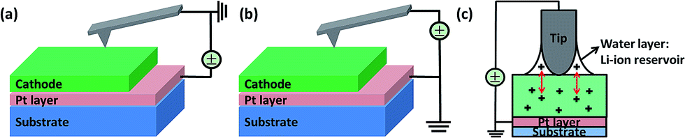 | ||
| Fig. 1 Schematic diagrams show the biased-AFM and c-AFM setups. (a) The c-AFM is conducted in contact mode and applies a dc voltage through the bottom electrode (Pt layer) and the tip was grounded. (b) The biased-AFM is operated in contact mode and a dc voltage is applied through the conductive tip whereas the bottom electrode (Pt layer) on substrate was grounded to ensure the circuit continuity. (c) Under ambient condition, there will be a formation of water layer at the tip–surface junction. This water meniscus can serve as Li-ion reservoir, and a nano-electrochemical cell can be formed at the tip–sample junction. In such a case, the Li-ions can move into or out-of the sample surface under the positive or negative bias (the positive signs represent positively charged Li-ions). | ||
Nanoscale mapping of conductance variations
Previous studies have reported that Li-ions movement and changes of the Li-ions concentration in cathode materials could cause the anomalous changes in electric conductance.9,10 High current indicates large amounts of Li-ions movement.15 Study on LiCoO2 has also shown that the electronic conductivity increased considerably upon Li-ion deintercalation process.32 It was known that LixCoO2 with x ≥ 0.94 was showed semi-conductive behavior while highly Li-deficient phase (0.35 ≤ x ≤ 0.75) exhibited metallic conductivity.33 For LiNi1/3Co1/3Mn1/3O2 material, the electrical conductivity was increased during first charge process and decreased during the discharge.19 Further study on the cathode material of Li1−xNi0.8Co0.15Al0.05O2 has also shown the electronic conductivity was increased with decreasing Li-content over the range of x = 0.0 to 0.6.34 These results suggested that high conductive region should correspond to the conductive Li-deficient locations (with fast Li-ions diffusion) under applied electrical field. Therefore, the mechanism of Li-ions diffusion may be demystified by studying the localized conductivity variations induced by electric field.In this work, the current maps have been obtained by c-AFM in the range of 0.5 V to 3 V with a step of 0.5 V over an area of 1.5 × 1.5 μm2. Further increasing the bias voltage, i.e., beyond 3.5 V, may cause deteriorated topography change in this material. This agrees well with the previous ESM (Electrochemical Strain Microscopy) study on the same cathode material, there was a significant change on topography between 3 and 4 V.29Fig. 2(a) shows the AFM topography image and Fig. 2(b) is the current image (under 3 V bias) overlaid on the topography image. There is a slight shift between the AFM and c-AFM images. Generally speaking, conductivity is defined as σ = (I/V)(l/A), where l is the distance between two points at which the voltage is measured and A is cross-sectional area perpendicular to the direction of the current. For a uniform material with a well-defined dimensions, the conductivity is proportional to the ratio of (I/V).10 In the c-AFM measurement of this study, the tip contact area and film thickness are generally fixed, also the external voltage is a constant through the measurement, hence the current variations can reflect the conductivity changes. The yellow-colored regions in current image correspond to locations with higher current (conductivity). Fig. 2(b) shows that the conductivity in most of the grain boundaries is much higher than that in the grain interiors. The current reduces further as the positions move away from grain boundaries. It is generally believed that the atoms located at grain boundaries are much more mobile than those inside the grains and hence the solute atoms can diffuse much faster along the grain boundary.35 The current differences between the grain interiors and boundaries are attributed to the differences in the Li-ions diffusion properties. As the grain boundaries can form a network within the material, therefore the electrochemical activity and diffusion of the Li-ions can be further enhanced at the grain boundaries. However, it is also noticed that not all the grain boundaries show higher current. For example, the current is lower at the boundaries of the five grains [marked by G1 to G5 in Fig. 2(a)]. This is probably because these grains are located at relatively higher position than other grains, as shown in the AFM topographic height images [Fig. 2(a)] where the bright regions correspond to the higher location. Therefore their grain boundaries may not be interconnected with other grains, hence, the conductivity of these grain boundaries are reduced.
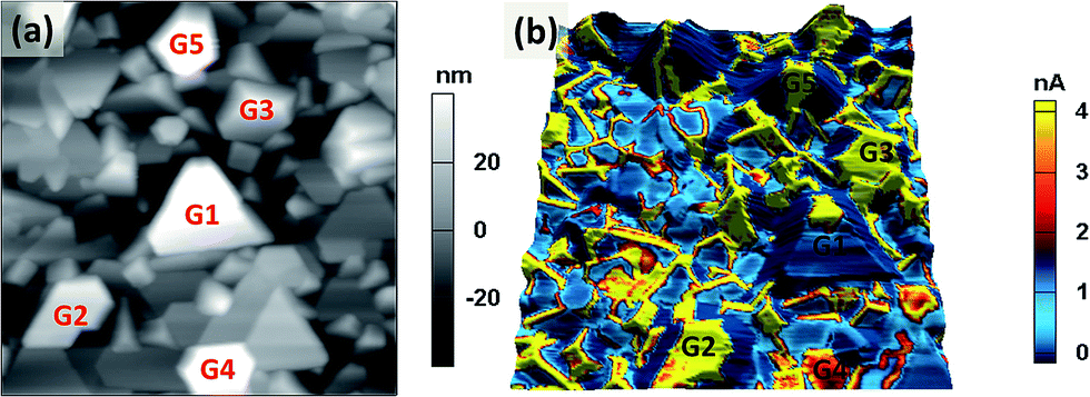 | ||
| Fig. 2 The corresponding height and current variations in the Li1.2Co0.13Ni0.13Mn0.54O2 cathode thin film over the scanning area of 1.5 × 1.5 μm2: (a) AFM height image; and (b) c-AFM current image (3 V) overlaid on the AFM topography image. The grains marked with G1 to G5 show higher location in the topography image and their boundaries show lower current. | ||
Fig. 3 shows the changes of the current images with increasing bias from 0.5 V to 3 V. Again, the bright regions in current images correspond to the more conductive location. Within the range of 0.5 V to 1 V [Fig. 3(a) and (b)], the current can only be detected in few grains and most of grains show lower current. Further increasing the bias to 1.5 V [Fig. 3(c)], the conductive regions increase with certain grain boundaries showing high current value. When the bias reaches to 2 V [Fig. 3(d)], the current level of the grain boundaries increases abruptly. With further increasing the bias to 3 V [Fig. 3(d) to (f)], the current within the whole scanning area increases significantly. More importantly, high current position extends from grain boundaries to the grain interiors. Fig. 3(g) shows the comparison of current line section profiles along the lines in the images (d) to (f), respectively. Current between the grain interiors and boundaries changes from ∼1 nA to ∼5 nA when the bias changes from 2 V to 3 V. The width of the high current peaks also increases [Fig. 3(g)], this further confirms the extension of conductive regime from the grain boundaries to interiors.
 | ||
| Fig. 3 The changes of the current in Li1.2Co0.13Ni0.13Mn0.54O2 cathode thin film under various electrical fields over the scanning area of 1.5 × 1.5 μm2. (a) to (f) are the current images scanned with the bias of 0.5 V, 1 V, 1.5 V, 2 V, 2.5 V and 3 V, respectively; and (g) is the current profile along the lines in the images (d) to (f), respectively. | ||
Local probing of conductance characteristics in an individual grain studied by I–V measurement
The local conductance characteristics at different locations within one grain are studied by measuring the I–V (current–voltage) curves using bipolar triangular voltage sweep. Fig. 4(a) shows the topography of one investigated grain, where the five measured points are also shown. Fig. 4(b) shows the waveform of the biases applied (two ±8 V triangular bias sweeps applied with a sweep frequency of 1 Hz). Fig. 4(c) shows the current as a function of time obtained from measurements at various locations during the voltage sweeps. All the locations show similar trends of conductance change. The current response in Fig. 4(c) is symmetric and consistent with the change of the voltage pulses. After initiating lithium ion redistribution by applying a sweep of the positive bias, the current response is reproducible with the sweep of the negative bias. Moreover, the probed current is repeatable over multiple cycles. This demonstrates that Li-ions can be redistributed reversibly within the grain, and the grain structure is stable. Furthermore, it can be clearly seen that when the tip is located further away from grain boundary, the current is further reduced; and this indicates less amounts of Li-ions can be induced far away from the grain boundary. Fig. 4(d) shows the corresponding I–V curve at different locations. The voltage that initiates the current increases with the distance from the grain boundary, and hence, this voltage may reflect the energy barrier for Li-ions diffusion at that location. Therefore, this result indicates the energy barrier for Li-ions diffusion increases with the distance from the grain boundaries.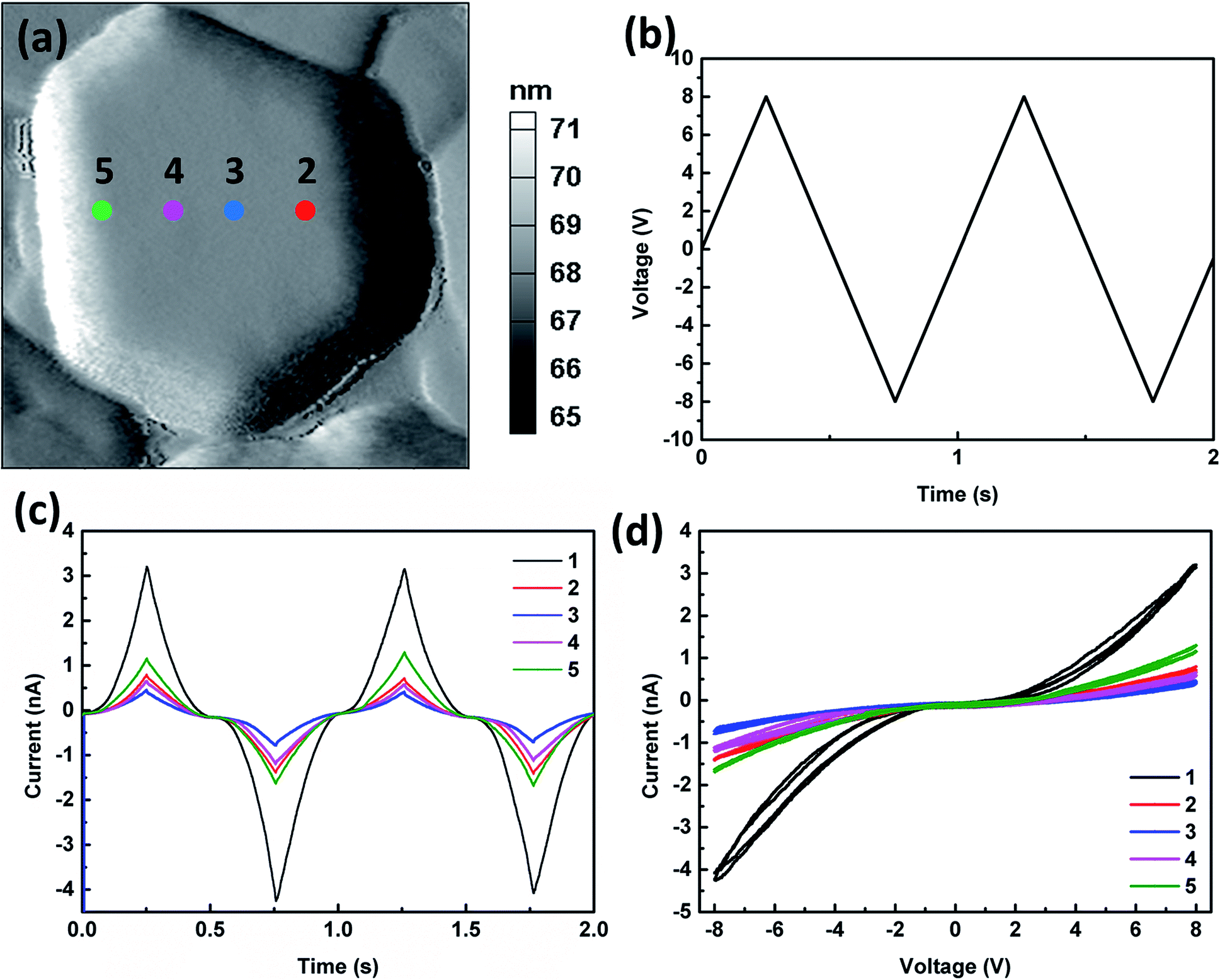 | ||
| Fig. 4 I–V curves at different locations away from boundaries: (a) AFM deflection image (0.2 × 0.2 μm2) of a selected grain with the marks (1 to 5) for tip locations (bias point); (b) the applied bias waveform; (c) current as a function of time at the five (5) locations marked in (a); and (d) corresponding I–V curves at the five locations marked in (a). | ||
This conductance characteristics in grains are further studied with the I–V measurement on the grains with different sizes. The tip is located at the center of the grains and the bias is applied with the same waveform which is shown in Fig. 4(b). Fig. 5(a) shows the topography of the investigated grains, where the four measured points are also shown. Fig. 5(b) shows the current as a function of time at the four locations during the voltage sweeps. As shown in Fig. 5(b), all grains show similar conductance change behaviors, except that the current level for the larger grains is smaller than that for the smaller grains at the same voltage. On the other hand, the current responses at different locations on one grain are further measured [Fig. 5(c) and (d)]. As shown in Fig. 5(d), when the tip is located near grain boundary (A to E), the conductance characteristics doesn't change much, almost independent of the tip locations. When the tip is located away from grain boundary (F to H), the current level becomes much lower, as shown in Fig. 5(d). Therefore, the results confirm that the conductance characteristics are closely dependent of the locations in a grain.
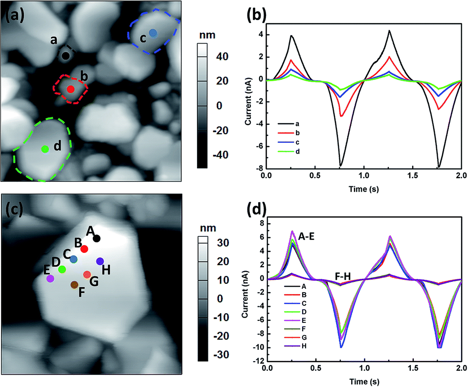 | ||
| Fig. 5 I–V curves at different locations: (a) AFM height image (1.1 × 1.1 μm2) where the center of four selected grains are marked (a to d) for tip locations; (b) current as a function of time at the four locations marked in (a); (c) AFM height image (0.5 × 0.5 μm2) where eight selected point are marked (A to F) for tip locations; and (d) current as a function of time at the eight locations marked in (c). | ||
Current mapping and I–V measurement in synthetic air and argon
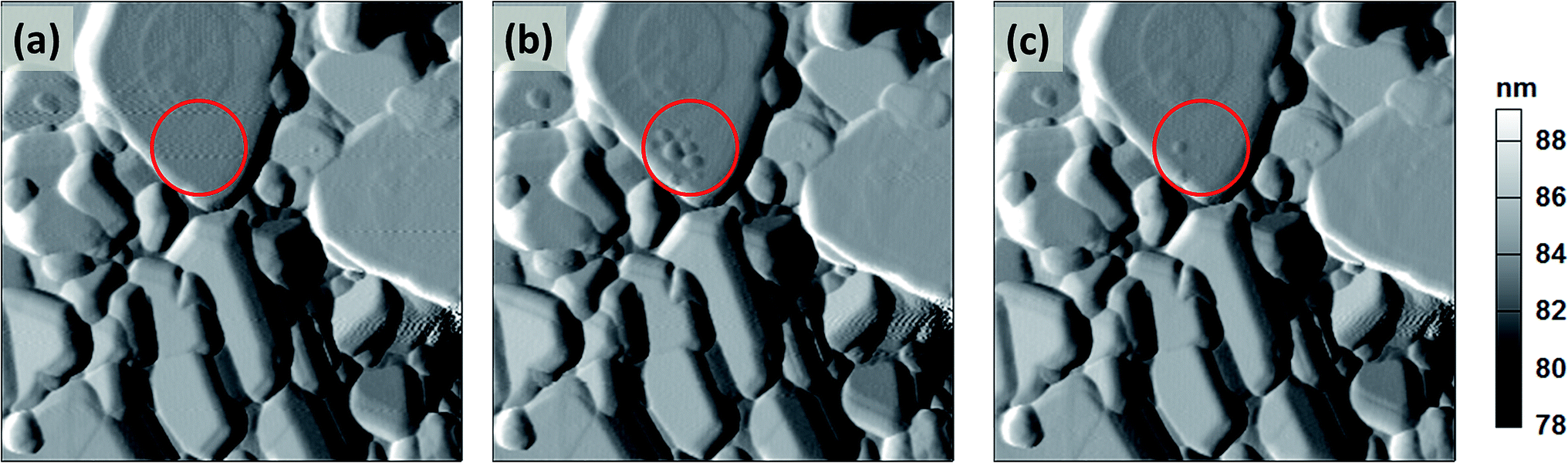
Further information about the kinetics and mechanism of the conductivity is obtained by conducting c-AFM measurements in the synthetic air and argon. Fig. 6 shows the current response of the thin film cathode in synthetic air and argon. It is noticed that almost no conductive region can be observed in the synthetic air [Fig. 6(a)] and argon [Fig. 6(b)]. Fig. 6(c) shows the applied bias voltage and the corresponding current response as a function of time in synthetic air and argon. Fig. 6(d) is the corresponding I–V curve. No current response is observed in the synthetic air and argon. Therefore, it can be concluded that, the lithium ion diffusion is greatly suppressed when the environment is absence of water, and electronic conductivity in the presence of water meniscus is consistent with a contribution from Li-ion diffusion. The role of adsorbed water may serve as “electrolyte” during the SPM measurements and suggests an electrochemical mechanism for the observed current initiation phenomenon. | ||
| Fig. 6 Current mapping and I–V measurement in synthetic air and argon. (a) c-AFM current image (3 V) in synthetic air; (b) current image (3 V) argon; (c) I–t and V–t in argon and synthetic air; (d) I–V curve in argon and synthetic air. | ||
In situ mapping of Li-ion intercalation/de-intercalation induced by positive and negative bias at grain boundary
In this study, biased-AFM technique is applied in the single point and the measurement is used to observe the surface topography changes induced by the localized Li-ions diffusion under the electric field. The effects of the positive or negative biases, as well as the effects of bias position are studied. After bias application, tapping mode AFM is immediately conducted to image the topography changes induced by bias.For comparison purposes, the positive biases are first applied at the grain interior for duration of 60 s. Fig. 7(a) to (c) are the deflection images scanned before applying the bias, immediately and 30 minutes after applying the +7 V bias at the same location. The biased position is located at the center of the red circle. Fig. 7(b) shows, after applying the +7 V bias at grain interior, several disperse protuberances emerge on the grain surface near the biased location. The features of other grains still remain the same as those before application of the bias. When positive bias is applied to the tip in biased-AFM, Li-ions are repelled away from the tip, resulting in a small region of depletion of Li-ions under the tip.36 The disperse protuberances indicate the evacuation of the Li-ions induced by positive bias since the c-axis of the lattice can expand as a result of increasing electrostatic repulsion between the TMO2 slabs due to the remove of the Li-ions.37 After 30 minutes, the dispersed protuberances disappear [Fig. 7(c)]. This indicates that Li-ions diffuse to the area with lower Li-ions concentration, resulting in the relaxation of Li-ions. In addition, although the chemical identification is not available due to the limitation of SPM, phase images still offer very useful information on the surface property and composition changes.16 Phase images show that the protuberances shift phase angle to a smaller value [Fig. S1, ESI†]. After 30 minutes, phase angle of the locations where protuberances once appear shift positively. This indicates the loss of Li-ions can shift the phase angle negatively. This result suggests a possible relationship between the Li-ions diffusion with the AFM phase images which need further investigations.
 | ||
| Fig. 7 Biased-AFM images of the Li1.2Co0.13Ni0.13Mn0.54O2 cathode when bias is applied insider the grain. The bias position is located at the center of the red circle (grain interior), and the scanning size is 1 × 1 μm2. (a)–(c) are the deflection images scanned before bias, immediately and 30 minutes after bias of +7 V. | ||
After this experiment, the bias was applied at selected grain boundaries region for duration of 60 s. Fig. 8(a) to (f) are the deflection images of the same area pre-biased, under 3 times of +7 V, followed by −7 V, and then +7 V bias again. The biased position is located at the gain boundary region (center of the red circle). Comparing with the pre-biased image, after applying +7 V bias for the first time at the grain boundary, those grains with flat facet (assuming with good crystallization), such as those marked by G1, G2 and G3, expand in a certain direction beyond the biased site, and it is found several steps emerge at certain grain boundaries [Fig. 8(b)]. On the other hand, the grains with round features such as that marked by G4, also beyond the biased site, but expand in all directions. The biased boundary only shows slightly morphological changes. When applying the +7 V bias for the second and third times, more and more steps begin to extrude along the same direction as those after the first bias [Fig. 8(c) and (d)]. Generally speaking, in the cathode with layered structure, the intercalation of Li-ions into cathode can cause an extension of the lattice in a-axis, while the de-intercalation of Li-ions out of the cathode can cause contraction of a-axis. In this work, since the cathode thin film is (003) orientated, the expanded grains and extruded steps (extension of a-axis) suggest that Li-ions move into these grains, causing the surface deformation, and this process should be similar to the intercalation process. Under the positive bias, lithium ions move into the cathode layer, hence causes the surface saturated with lithium ions and results in the volumetric expansion.31 With the application of the multiple times of biases, more Li-ions can be diffused into those grains. Compared with the observation where the bias is applied at grain interior, this result shows that Li-ions can diffuse into the surrounding grains through the interconnected grain boundaries. The boundary diffusion likely depends on the particular microstructure of the grain boundaries and the connectivity of the grains (or network). This result is consistent with the conductance map that shows certain grain boundaries can provide fast Li-ions diffusion pathways (Fig. 2). Additionally, Li-ions in the adjacent part can produce electrostatic repulsion to repulse those Li-ions driven by the tip bias, while the repulsive effect of electric field on Li-ions gradually decreases further away from tip–sample junction area. How far the Li-ions can be driven depends on the competitive electric field force and electrostatic repulsive force. Simulations and further experiment studies are still needed to provide more information on the interplay of electric field and electrostatic repulsion. In addition, such electrochemical behavior can be affected by the presence of a water meniscus that can both catalyze the electrochemical reaction and allow for increased ionic conduction. In order to confirm if above observation is caused by the water meniscus, the similar tests are performed in synthetic air and Ar gas (Fig. S2 and S3, ESI†). The results show that there is no deformation either in the biased position or surrounding area. These results confirm that the observed large deformation (Fig. 8) occur with the existing of water or moisture from the environment.
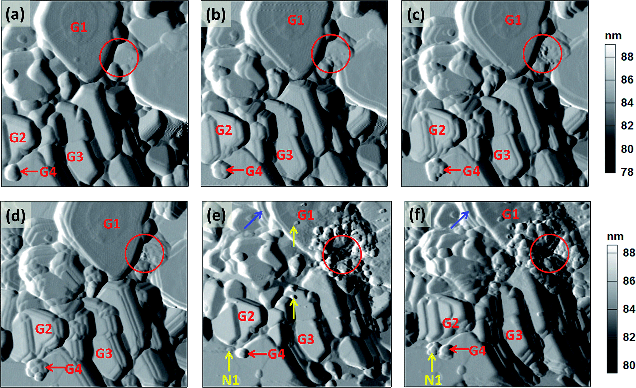 | ||
| Fig. 8 Biased-AFM images of the Li1.2Co0.13Ni0.13Mn0.54O2 cathode thin film when bias is applied at grain boundary. The biased position is located at the center of the red circle (grain boundary), and the scanning size is 1 × 1 μm2. Deflection images of the same area of: (a) before application of the bias; (b) 1st time under bias of +7 V; (c) 2nd time under bias of +7 V; (d) 3rd time under bias of +7 V; (e) under the bias of −7 V; and (f) under the bias of +7 V again. | ||
After applying the −7 V bias at the same location, the previously-formed extruded steps in unbiased area are vanished [Fig. 8(e)], and this is accompanied by the shrinkage of the grains (G1, G2 and G3). Note that the grain shape recovers to its original appearance but the grain size generally becomes smaller. Grain G4 also shrinks and becomes smaller. The shrinkage of the grains (contraction of a-axis) suggests Li-ions move out of these grains, and this process should be similar to the de-intercalation process. When the negative bias is applied, the “de-intercalation” occurs at the reservoir interface and volumetric shrinkage is induced.30,31 Therefore, the results in Fig. 8 suggest, when applying positive and followed by negative bias at the same location, Li-ions can reversibly “intercalated” into and “de-intercalated” out of the grains in the nearby locations. It is also noticed that the biased position [circled position in Fig. 8(e)] has been damaged after the application of the negative bias, whereas the nearby grains show reversible changes. There are some new and smaller nucleated particles at the biased location. This indicates the negative bias can induce extraction of Li-ions to the surface followed immediately by the precipitation of Li hydroxides and carbonates due to the direct reaction involved with Li and ambient moieties (H2O, O2, CO2, etc.).38,39 Furthermore, there are also some new grains formed beyond the biased location (marked by yellow arrows such as N1), and this indicates the possible exfoliation of the particles due to the “de-intercalation” of the Li-ions. Delamination is observed in grain G1 (marked by blue arrows), and it suggests non-uniform Li-ions “de-intercalation” in this grain. From a full-cell battery point of view, exfoliation and delamination due to non-uniform Li-ions diffusion may cause loss of contact between the cathode and electrolyte, and this can lead to the aging of the battery. Comparing with the results in synthetic air and Ar gas, again, there is no deformation observed at surface under negative bias (Fig. S2 and S3, ESI†). These results are also consistent with what reported on Li1.2Co0.13Ni0.13Mn0.54O2 particles.15
A bias of +7 V is then applied again at the same location, and the topography images are shown in Fig. 8(f). It is observed that most of the grains expand again and new steps are extruded from the grain structure, this indicates the “re-intercalation” of the Li-ions under the positive bias. However, the topography changes due to Li-ions “re-intercalation” are different from those caused by the first Li-ions “intercalation” process [Fig. 8(b)]. The extruded steps are not well arranged as those formed during the first Li-ions “intercalation” process. For example, the grain G2 expands again but becomes delaminated; grain G3 also expands but in a different direction; and the grain G4 expands but to a much smaller degree. The newly formed grain N1 (during the −7 V bias) does not disappear but expands obviously. The grain G1 still remains delaminated and does not recover to its initial state as an integrated grain. These unrecoverable topography changes imply the degradation and structural changes of the cathode material during the “intercalation” and “de-intercalation” processes. This experiment has provided a new perspective for understanding the underlying mechanisms of the poor cycling performance of the cathode in a full-cell battery system.
Furthermore, phase images and distribution histogram of phase angles (data fitted by using Gaussian function theory) show that the average phase angle shifts positively after Li-ions “intercalation” and negatively after Li-ions “de-intercalation” processes [Fig. S4, ESI†]. After 2nd Li-ion “intercalation” process, phase angle shift positively again. During the AFM measurement, phase angle shift was primarily originated from the difference in mechanical properties, such as elastic modulus, surface hardness and adhesion energy.16,40,41 Due to the complex interpretation of phase images, the precise explanation for the relationship between phase angle shift and Li-ion concentration is still a challenge issue and need to be studied further. However, this study indicate that the possible relationship between phase angle shift and Li-ion concentration. Since the characterization on Li-ion concentration is very significant for in situ SPM studies on the LIB materials, more efforts should be put to investigate the relationships between the phase values and Li-ion content in the future studies.
The biased-AFM results indicate that the Li-ion diffusion under the biases is different along the grain boundary and within the grain interior. More specifically, the bias applied at grain interior can only cause localized Li-ions diffusion inside the grain, whereas the bias applied at grain boundary can cause the Li-ions “intercalation” into and “de-intercalation” out of the surrounding grains reversibly. This is due to the fact that grain boundaries can form a continuous network in polycrystalline materials, and this network can provide a fast diffusion path for ion diffusion.
Conclusions
In summary, this paper has studied the grain boundary effects on the Li-ion diffusion at nanoscale in Li1.2Co0.13Ni0.13Mn0.54O2 thin film cathode by using SPM-based techniques, namely c-AFM, biased-AFM and AFM. Firstly, the conductivity variations between the grain interior and grain boundaries are investigated by using c-AFM measurements. Grain boundaries are more conductive than that of the grain interiors, and this indicates the enhanced Li-ions diffusion at grain boundaries. With increasing the bias voltage, the high conductive regimes extend from grain boundaries to the grain interiors. I–V curve measurements also show decreased current and increased voltage for current initiation when the tip moves away from the boundaries. These results indicate larger amount of Li-ions can be induced near the grain boundary and the energy barrier for Li-ions movement is lower as the distance from the grain boundaries decreases. In addition, current mapping and I–V measurement are conducted in synthetic air and argon. No current response is observed in synthetic air and argon. This suggests an electrochemical mechanism of the observed electronic conductivity. Secondly, the topography changes corresponding to the bias locations are examined by biased-AFM measurements. Bias applied at the grain boundaries can induce more dramatic topography changes than that at the interiors. Therefore, optimization of the interconnectivity of grain boundary network can provide a direct approach to facilitate Li-ions diffusion in electrode materials, and further to improve the electrochemical performance for LIB systems. This result also has the implication of the importance of controlling of the grain size in the cathode materials.Moreover, this work has applied the positive and negative biases in sequence at a single-point to visualize the processes of the Li-ions move into and out, i.e., similar to the “intercalation” and “de-intercalation” processes, the layered structure in the cathode film without assembly of a full-cell battery system. In addition, exfoliation and delamination, degradation and structural changes of the cathode material are observed during the Li-ions movements. These observations at the nanoscopic scale offer valuable insights into the elucidation of aging mechanisms of cathode materials in a realistic battery device. This work also shows that the in situ characterization of the local electrochemical phenomena can afford clues to improve the performance of LIB systems.
Acknowledgements
This work is supported by Ministry of Education (Singapore) through National University of Singapore under Academic Research Fund (R-265-000-406-112). One of the author (YS) would also like to thank the support of scholarship by Ministry of Education (Singapore) under the Academic Research Fund (R-265-100-406-112).References
- A. Manthiram, J. Phys. Chem. Lett., 2011, 2, 176–184 CrossRef CAS.
- B. Scrosati and J. Garche, J. Power Sources, 2010, 195, 2419–2430 CrossRef CAS.
- P. Kurzweil and K. Brandt, in Encyclopedia of Electrochemical Power Sources, ed. J. Garche, Elsevier, Amsterdam, 2009, pp. 1–26 Search PubMed.
- S. V. Kalinin and N. Balke, Adv. Mater., 2010, 22, E193–E209 CrossRef CAS PubMed.
- N. Balke, S. Jesse, A. N. Morozovska, E. Eliseev, D. W. Chung, Y. Kim, L. Adamczyk, R. E. Garcia, N. Dudney and S. V. Kalinin, Nat. Nanotechnol., 2010, 5, 749–754 CrossRef CAS PubMed.
- N. Balke, S. Kalnaus, N. J. Dudney, C. Daniel, S. Jesse and S. V. Kalinin, Nano Lett., 2012, 12, 3399–3403 CrossRef CAS PubMed.
- N. Balke, S. Jesse, Y. Kim, L. Adamczyk, A. Tselev, I. N. Ivanov, N. J. Dudney and S. V. Kalinin, Nano Lett., 2010, 10, 3420–3425 CrossRef CAS PubMed.
- A. Nevosad, M. Hofstaetter, M. Wiessner, P. Supancic and C. Teichert, Oxide-Based Materials and Devices IV, 2013, vol. 8626, p. 862618 Search PubMed.
- K. Kuriyama, A. Onoue, Y. Yuasa and K. Kushida, Surf. Sci., 2007, 601, 2256–2259 CrossRef CAS.
- X. Zhu, C. S. Ong, X. Xu, B. Hu, J. Shang, H. Yang, S. Katlakunta, Y. Liu, X. Chen, L. Pan, J. Ding and R. W. Li, Sci. Rep., 2013, 3, 1084 Search PubMed.
- T. M. Arruda, A. Kumar, S. V. Kalinin and S. Jesse, Nano Lett., 2011, 11, 4161–4167 CrossRef CAS PubMed.
- T. M. Arruda, A. Kumar, S. Jesse, G. M. Veith, A. Tselev, A. P. Baddorf, N. Balke and S. V. Kalinin, ACS Nano, 2013, 7, 8175–8182 CrossRef CAS PubMed.
- R. Kostecki and F. McLarnon, Electrochem. Solid-State Lett., 2002, 5, A164–A166 CrossRef CAS.
- R. Kostecki and F. McLarnon, Electrochem. Solid-State Lett., 2004, 7, A380–A383 CrossRef CAS.
- T. Li, B. Song, L. Lu and K. Zeng, Phys. Chem. Chem. Phys., 2015, 17, 10257–10264 RSC.
- J. Zhu, J. Feng, L. Lu and K. Zeng, J. Power Sources, 2012, 197, 224–230 CrossRef CAS.
- J. Zhu, K. Zeng and L. Lu, J. Appl. Phys., 2012, 111, 063723 CrossRef.
- S. K. Jeong, M. Inaba, Y. Iriyama, T. Abe and Z. Ogumi, J. Power Sources, 2003, 119–121, 555–560 CrossRef CAS.
- X. Y. Qiu, Q. C. Zhuang, Q. Q. Zhang, R. Cao, Y. H. Qiang, P. Z. Ying and S. G. Sun, J. Electroanal. Chem., 2012, 687, 35–44 CrossRef CAS.
- J. Vetter, P. Novák, M. R. Wagner, C. Veit, K. C. Möller, J. O. Besenhard, M. Winter, M. Wohlfahrt-Mehrens, C. Vogler and A. Hammouche, J. Power Sources, 2005, 147, 269–281 CrossRef CAS.
- M. Wohlfahrt-Mehrens, C. Vogler and J. Garche, J. Power Sources, 2004, 127, 58–64 CrossRef CAS.
- J. B. Bates, N. J. Dudney, B. J. Neudecker, F. X. Hart, H. P. Jun and S. A. Hackney, J. Electrochem. Soc., 2000, 147, 59–70 CrossRef CAS.
- H. Xia and L. Lu, Electrochim. Acta, 2007, 52, 7014–7021 CrossRef CAS.
- H. Moriwake, A. Kuwabara, C. A. J. Fisher, R. Huang, T. Hitosugi, Y. H. Ikuhara, H. Oki and Y. Ikuhara, Adv. Mater., 2013, 25, 618–622 CrossRef CAS PubMed.
- L. Li, K. S. Lee and L. Lu, Funct. Mater. Lett., 2014, 07, 1430002 CrossRef.
- H. Koga, L. Croguennec, P. Mannessiez, M. Ménétrier, F. Weill, L. Bourgeois, M. Duttine, E. Suard and C. Delmas, J. Phys. Chem. C, 2012, 116, 13497–13506 CAS.
- M. M. Thackeray, S. H. Kang, C. S. Johnson, J. T. Vaughey, R. Benedek and S. A. Hackney, J. Mater. Chem., 2007, 17, 3112–3125 RSC.
- B. Yan, J. Liu, B. Song, P. Xiao and L. Lu, Sci. Rep., 2013, 3, 3332 Search PubMed.
- S. Yang, B. Yan, T. Li, J. Zhu, L. Lu and K. Zeng, Phys. Chem. Chem. Phys., 2015, 17, 22235–22242 RSC.
- N. Balke, S. V. Kalinin, A. Morozovska and E. Eliseev, J. Appl. Phys., 2010, 108, 053712 CrossRef.
- D. W. Chung, N. Balke, S. V. Kalinin and R. E. Garcia, J. Electrochem. Soc., 2011, 158, A1083–A1089 CrossRef CAS.
- M. Menetrier, I. Saadoune, S. Levasseur and C. Delmas, J. Mater. Chem., 1999, 9, 1135–1140 RSC.
- T. Motohashi, Y. Sugimoto, Y. Masubuchi, T. Sasagawa, W. Koshibae, T. Tohyama, H. Yamauchi and S. Kikkawa, Phys. Rev. B: Condens. Matter Mater. Phys., 2011, 83, 195128 CrossRef.
- R. Amin, D. B. Ravnsbæk and Y. M. Chiang, J. Electrochem. Soc., 2015, 162, A1163–A1169 CrossRef CAS.
- M. Park, X. Zhang, M. Chung, G. B. Less and A. M. Sastry, J. Power Sources, 2010, 195, 7904–7929 CrossRef CAS.
- T. M. Arruda, A. Kumar, S. V. Kalinin and S. Jesse, Nanotechnology, 2012, 23, 325402 CrossRef PubMed.
- A. Clémençon, A. T. Appapillai, S. Kumar and Y. Shao-Horn, Electrochim. Acta, 2007, 52, 4572–4580 CrossRef.
- T. M. Arruda, A. Kumar, S. V. Kalinin and S. Jesse, Nano Lett., 2011, 11, 4161–4167 CrossRef CAS PubMed.
- A. Kumar, T. M. Arruda, A. Tselev, I. N. Ivanov, J. S. Lawton, T. A. Zawodzinski, O. Butyaev, S. Zayats, S. Jesse and S. V. Kalinin, Sci. Rep., 2013, 3, 1621 Search PubMed.
- S. Thanawan, S. Radabutra, P. Thamasirianunt, T. Amornsakchai and K. Suchiva, Ultramicroscopy, 2009, 109, 189–192 CrossRef CAS PubMed.
- S. N. Magonov, V. Elings and M. H. Whangbo, Surf. Sci., 1997, 375, L385–L391 CrossRef CAS.
Footnote |
| † Electronic supplementary information (ESI) available: Biased-AFM phase images (bias is applied at grain interior) of the Li1.2Co0.13Ni0.13Mn0.54O2 cathode thin film; biased-AFM phase images (bias is applied at grain boundary) of the Li1.2Co0.13Ni0.13Mn0.54O2 cathode thin film. See DOI: 10.1039/c6ra17681j |
| This journal is © The Royal Society of Chemistry 2016 |