DOI:
10.1039/C6RA17668B
(Paper)
RSC Adv., 2016,
6, 78702-78713
Low temperature processed graphene thin film transparent electrodes for supercapacitor applications†
Received
11th July 2016
, Accepted 1st August 2016
First published on 2nd August 2016
Abstract
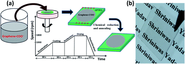
The highest conductivity in graphene oxide based thin film electrodes has been achieved using high temperature annealing at 1100 °C. This is unfavorable for low cost production and application over plastic substrates. Here we report highly conducting graphene thin films using spin coating of a functionalized graphene solution over various substrates. The bridged graphene nanoflakes provide higher conducting pathways in the thin film, enabling electrodes to be fabricated at low temperatures of the order 150 °C. These thin film electrodes show remarkable sheet resistance of the order 0.4 kΩ sq.−1 and transmittance up to 94%. This work demonstrates that graphene based transparent electrodes have the potential to replace existing doped metal oxide based electrodes. The electrochemical performance of graphene thin films as active supercapacitor electrodes was evaluated using cyclic voltammetry. The calculated specific capacitance was found to be ≈49, 48, 48 and 68 F g−1 for the graphene thin film electrodes fabricated at spin speeds of 1000, 1200, 1400 and 1600 rpm, respectively. The above electrochemical performance indicates that the graphene electrodes show large specific capacitance and could be very attractive for several applications including wearable electronics, smart windows and advanced display panels.
1. Introduction
Inspite of having the highest conductivity along with a transparency of the order 97.7%, graphene has a very stretchable crystal structure, as a result of which, it can be used as an alternative for metal oxide based flexible and transparent electrodes.1 So far, much effort has been made to fabricate thin films of graphene over transparent substrates. Various methods, i.e. chemical vapor deposition (CVD),2,3 dip coating,4 spin coating,5 vacuum filtration,6 Langmuir–Blodgett deposition7 and spray coating,8 have been explored for the fabrication of graphene thin films. The CVD method has been recognized as one of the most promising processes for generating high quality graphene films, for electronic and optoelectronic devices. Various researchers have reported fabrication of large area monolayer and bilayer graphene films using CVD with lower sheet resistances and higher transmittances.
The high cost, low throughput and complications associated with transfer of CVD grown graphene films from catalysis substrates to desired substrates makes this process limited for scaling up. Further, graphene thin film electrodes are fabricated from graphene oxide suspensions by solution processing. In order to get a sheet resistance less than 100 Ω sq.−1, the substrate is annealed at 1100 °C.9 This high temperature annealing makes the process costly, incompatible for plastic substrates and unsuitable for multijunction device fabrication. Various papers report thin films of graphene and carbon nano tube (CNT) based hybrids.10 Incorporation of CNTs with graphene lowers the sheet resistance many folds without affecting the transparency much.10 But in case of CNT-graphene hybrid films, it is very challenging to keep the proper alignment of the CNTs. Also, if we proceed towards patterning graphene and CNT based composite films, selective etching is very challenging since both the materials have different etching conditions. Hence, fabricating thin films of only graphene with a lower sheet resistance and higher transparency is the biggest challenge for practical device fabrication.
Herein we report a layer by layer (LBL) spinning of functionalized graphene sheets over various substrates. We have functionalized graphene with carboxylic and amine groups to generate partial negative and positive charges over the surface. Substrates are coated via 3-aminopropyltriethoysilane (APTES) followed by spin coating of negatively and positively charged graphene suspensions with optimized concentrations in deionized (DI) water. Film thickness is controlled by varying spinning rpm. Sheet resistance and transmittance of the film, which depends upon thickness, are plotted as a function of spinning rpm at a constant time. We have achieved a sheet resistance of the order 0.4 kΩ sq.−1 and transmittance of the order of 94%. Properties of graphene thin films intensely depend upon various factors like the quality of the material, aspect ratio, surface area of graphene, etc. The obtained results can be improved by improving the above parameters. The calculated ratio of DC conductivity and optical conductivity (σdc/σopt), also known as the figure of merit of transparent conductors, is 4.78 for electrodes fabricated at 1000 rpm. Figure of merit values, for graphene based thin films made by different methods are tabulated in the ESI (Table 1†). Fabricated films consist of bridging graphene flakes in one layer by another layer. This patching of graphene layers over other layers enables more conduction pathways. This results in the low temperature fabrication of graphene thin films. The maximum specific capacitance was found to be 68 F g−1 for the graphene thin film electrode fabricated at a spin speed of 1600 rpm. Tao Chen et al. reported a graphene based transparent and stretchable supercapacitor with a specific capacitance of 7.6 F g−1 along with a transparency of 60% at the wavelength 550 nm.11 In another research paper, T. Chen et al. reported a transparent supercapacitor with a specific capacitance of 7.3 F g−1 and transmittance up to 75% at the wavelength of 550 nm using highly aligned carbon nanotube sheets.12 Recently, X. Y. Liu et al. reported a flexible and transparent supercapacitor based on ultrafine Co3O4 nanocrystal electrodes with a higher specific capacitance, of the order 177 F g−1, and an optical transmittance of up to 51% at a wavelength of 550 nm.13
From the above references we can see that transparent supercapacitors have either a higher specific capacitance or a higher transmittance. But in our work, we are reporting graphene based transparent electrodes with a very high optical transmittance, of the order 94% at a wavelength of 550 nm, and a good specific capacitance, of the order 68 F g−1. Also, in this work we are using graphene thin films without any metal current collector for supercapacitor performance evaluation. So there is still considerable space for further improvement in energy storage performance through optimization of the device structure.
2. Experimental
2.1. Materials
The single layer graphene used in this work was purchased from ACS materials, USA; other chemicals like H2SO4, HNO3, APTES, ethylenediamine, liquor ammonia, 1-ethyl-3-(3-dimethylaminopropyl) carbodiimide (EDC) and anhydrous hydrazine were purchased from Merck & Co., Inc., (India). Polyethylene terephthalate (PET) sheets were purchased from Sigma Aldrich, India. All the materials used in the present study were of analytical grade.
2.2. Preparation of negatively charged graphene solution
For carboxylation, graphene (15 mg) was treated with H2SO4
:
HNO3 in a 1
:
3 ratio by ultrasonicating for 15 minutes in an ice bath.10,14 After ultrasonication, DI water was added into the mixture and kept for 30 minutes at room temperature. Then, the solution was filtered and washed five times with 18 MΩ DI water through a hydrophilic filtration membrane (0.22 μm, pore size). Filtered graphene was re-dispersed in DI water and the solution was centrifuged 5 times at 2000 rpm for two minutes to remove all the insoluble particles. The supernatant solution was diluted to 1.5 mg mL−1 and used for further experimentation. Fourier transform infrared (FTIR) characterization of carboxylic acid functionalized graphene (G-COOH) is given in the ESI (Fig. S3†).
2.3. Preparation of positively charged graphene solution
Positively charged graphene was synthesized according to the published protocol.10 A suspension of carboxylated graphene (100 mL, 0.15 mg mL−1) was reacted with ethylenediamine (3.0 mL) under stirring for 5 h in the presence of 300 mg of EDC and 0.5 mL liquor ammonia. The resulting suspension was sonicated for 30 minutes prior to vacuum filtration. Filtered graphene was re-dispersed in DI water and the solution was centrifuged 5 times at 2000 rpm for two minutes to remove all the insoluble particles. The supernatant solution was diluted to 1.5 mg mL−1 and used for further experimentation. FTIR characterization of amide functionalized graphene (NH2-G) is given in the ESI (Fig. S4†).
2.4. Substrate surface modification
Silicon and quartz substrates were cleaned with a piranha solution (H2O2/H2SO4, 1
:
3 v/v) to remove any organic contamination and treated with APTES to introduce a hydrophilic surface. Typically, 10 mL of APTES solution in toluene (v/v, 1
:
10) was prepared. Cleaned silicon and quartz substrates were immersed in the APTES solution for 30 minutes and washed thoroughly in toluene, acetone, ethanol and DI water respectively. After washing, the substrates were dried for four hours at 50 °C and used for further experiments.
2.5. Spin coating of G-COOH solution over substrate
G-COOH solution was spin coated at different spin speeds, from 1000 to 1600 rpm, for 30 seconds. To optimize the concentration of the G-COOH solution, six different concentrations, 0.5–3 mg mL−1, of G-COOH in DI water were taken and spin coated at 1000 rpm for 30 seconds. Then we tested these films for electricity conduction at different points using a multimeter. We got better results for the films made using the 1.5 mg mL−1 concentration solution. We have chosen this concentration for further experiments.
The spin-coating rate was increased from an initial value of 500 to a final value in 30 seconds to gradually spread the water dispersion on the surface, then kept at a constant final rpm for 30 seconds to uniformly overcoat the surface, and then finally raised it to 1800 rpm to dry the film. A schematic illustration of the spin coating process is shown in Fig. 1a. Residual water was removed by heating the films to 100 °C in a vacuum oven for several hours. The resulting G-COOH films were chemically reduced by dipping them in a hydrazine solution (1
:
5, v/v in DI water) for 1 hour at 80 °C. The resulting hydrazine treated graphene films were thermally reduced by vacuum annealing at 150 °C for 6 hours.
 |
| Fig. 1 (a) Schematic of G-COOH thin film fabrication by spin coating process. (b) Optical image of thin film coated quartz substrate. | |
2.6. Electrostatic incorporation of NH2-G on the G-COOH coated substrate
A NH2-G solution was spin coated over the G-COOH substrates at 1600 rpm for 30 seconds. After coating, the substrates were washed with DI water, and dried in a vacuum oven at 100 °C for several hours, to stabilize the interfaces among the substrate, the G-COOH, and the NH2-G. The G-COOH/NH2-G thin films were immersed in a hydrazine solution (1
:
5, v/v in water) for 1 hour at 80 °C, washed with water and then dried in a vacuum oven at 100 °C. The hydrazine-treated substrates were annealed under vacuum at 150 °C for 6 hours.
3. Results and discussion
To introduce graphene into the electrostatic LBL network, negatively and positively charged graphene were created via chemical functionalization. Negatively charged graphene was prepared by carboxylation with extremely aggressive acids, which could render oxygen containing carboxylic acid group on the graphene edges. In an aqueous solution, carboxylic acid groups on the graphene edges exist as carboxylate anion (COO−) yielding negatively charged graphene. Positively charged graphene was prepared by amidation of carboxylated graphene through the formation of amide bonds with G-COOH and ethylene diamine in the presence of thiourea. The surface charges over graphene not only keep it dispersed in solution but are also required for networking of the flakes. Large-area G-COOH were spin coated on a SiO2/Si and quartz substrate surface modified with an APTES self-assembled monolayer (SAM) to enhance the attractive force between the substrate and the G-COOH flakes. It revealed the effects of the electrostatic interaction between the SAM-modified surface and the G-COOH flakes.
3.1. Fabrication of G-COOH thin films
G-COOH thin films were prepared using a spin coating process. A 1.5 mg mL−1 G-COOH solution was spin coated at different spin speeds from 1000 to 1600 rpm for 30 seconds. The resulting G-COOH films were chemically reduced by dipping them in a hydrazine solution (1
:
5, v/v in DI water) for 20 minutes. The reduction of graphene oxide by hydrazine vapors is a well-known process.15–17 During chemical reduction, some bubbles form along the graphene surface, which is likely due to the production of NO2 and N2 as byproducts. The resulting hydrazine treated graphene films were thermally reduced by vacuum annealing at 150 °C for 6 hours. A schematic representation for the G-COOH/NH2-G film fabrication and optical image of the film over the quartz substrate is shown in Fig. 1a and b respectively.
3.2. Characterization of G-COOH thin films
The above prepared films are characterized for transmission in the wavelength range from 300 to 800 nm (Fig. 2a) using a double beam UV-vis-NIR spectrophotometer (Cary 5000) on a transparent quartz substrate. As can be seen from the transmittance vs. wavelength plot, G-COOH films are more transparent towards the NIR regions; this is different as in the case of ITO based electrodes having less transmittance towards the NIR region.1 This makes graphene more interesting for NIR based device applications. Transmittance also increases with an increase in the spin speed, as film thickness decreases with an increase in the spin speed, allowing a larger number of visible photons to pass through. G-COOH films fabricated at spin speed of 1000, 1200, 1400 and 1600 rpm showed optical transmittances of 85.8, 86.5, 88.7 and 94.6% respectively, at 550 nm.
 |
| Fig. 2 Various characteristics plots of G-COOH films at different spin speeds. (a) Transmission spectrum in wavelength range of 300–800 nm (b) sheet resistance vs. spin speed plot. (c) Sheet resistance vs. transmittance at 550 nm plot. (d) σdc/σopt plot. | |
Four point sheet resistance measurements (Keithley, SCS 4200) were made over the same films after deposition of small fingers of conductive silver paste. Sheet resistance also increases with increasing spin speed. Higher spin speeds provide thinner films, which are less electrically conductive due to a smaller number of conduction pathways for the flow of electrons. The G-COOH films showed sheet resistance of 5.36, 12.76, 17.30 and 22.48 kΩ sq.−1 corresponding to spin speeds of 1000, 1200, 1400 and 1600 rpm, respectively (Fig. 2b). A plot between the sheet resistance and the transmittance at 550 nm for different spin speed is shown in Fig. 2c. Both sheet resistance and transmittance increase with an increase in spin speed.
In order to use graphene based thin films as transparent electrodes, it is desirable to have a high optical transmission with a low sheet resistance. This corresponds to films with low optical conductivity (σopt) and high direct current conductivity (σdc). An approximate relationship between the optical transmittance, sheet resistance, σdc and σopt is given by the following relation:10,18
|
 | (1) |
|
 | (2) |
The ratio of the direct current conductivity to the optical conductivity (σdc/σopt), which is considered as a figure of merit for transparent conductors, is calculated using the above mentioned equations. Measured value of σdc/σopt vs. spin speed for different films are shown in Fig. 2d. The G-COOH film fabricated at 1000 rpm shows a maximum value for σdc/σopt of 0.44, corresponding to a transmittance of 85.8% at λ = 550 nm and a sheet resistance of 5.36 kΩ sq.−1. The σdc/σopt value decreases with increasing spin speeds due to a significant enhancement of the sheet resistance with spin speed compared to the enhancement in the transmittance, except for the film made at 1600 rpm where the transmittance is increasing significantly compared to the sheet resistance (Fig. 2a).
The structural morphology of the G-COOH films was measured by a non-contact mode atomic force microscope (NCAFM, XE-100, Park systems, Korea) with a backside-gold-coated silicon probe. Fig. 3 is the atomic force microscope (AFM) images along with the 3D surface topography, and line profile for the films fabricated at different spin speeds (top to bottom images corresponds to film fabricated at spin speed from 1000 to 1600 rpm). AFM images show that the G-COOH films are composed of mainly single/double-layered graphene flakes and a few of multi-layered graphene. The AFM image reveals that there are various uncovered voids within the graphene sheets which may disturb the current conduction pathways resulting in a higher sheet resistance.
 |
| Fig. 3 The AFM image of G-COOH films fabricated over quartz substrates with height profiles measured by line scans and 3D topographic views (top to bottom images corresponds to film fabricated at spin speed from 1000 to 1600 rpm). | |
3.3. Fabrication of G-COOH/NH2-G thin films
G-COOH/NH2-G films were fabricated by spinning a NH2-G solution over the G-COOH substrates at 1600 rpm for 30 seconds. After spinning, functionalized graphene was reduced to graphene through hydrazine treatment to improve the material's electrical conductivity.19 It is reported that hydrazine treatment is not sufficient to achieve maximum reduction and annealing alone requires high temperatures.20 Therefore, we achieved efficient reduction through a combination of hydrazine treatment and low temperature annealing process.21
After the chemical and thermal treatment, these films were subjected to electrical and optical characterization. A schematic representation of the G-COOH/NH2-G film fabrication and optical image of the film over a quartz substrate are shown in Fig. 4a and b respectively.
 |
| Fig. 4 (a) Schematic of G-COOH/NH2-G thin film fabrication by a spin coating process. (b) Optical image of the thin film coated quartz substrate. | |
3.4. Characterization of G-COOH/NH2-G thin films
The transmittance spectra of G-COOH/NH2-G films fabricated at different spin speeds are shown in Fig. 5a. Films fabricated at 1000, 1200, 1400 and 1600 rpm show transmittances of 84.1, 85.4, 87.8 and 94.2% respectively. Fig. 5b shows sheet resistance plot. The sheet resistance increases with an increase in the spin speed. For 1000, 1200, 1400 and 1600 rpm, the sheet resistances observed are 0.34, 0.59, 0.72 and 1.87 kΩ sq.−1 respectively. The fabricated G-COOH/NH2-G thin films showed an improved conductivity by 10–15 fold compared to the G-COOH films, without much decrease in transparency. This may be attributed to the small light diffuse reflectance and scattering effects associated with homogenous coverage of G-NH2 over G-OOH thin films.22 The homogenous networked structure of G-COOH/NH2-G films can be observed from scanning electron microscope (SEM) and AFM images (Fig. 6 and 7).
 |
| Fig. 5 Various characteristic plots of G-COOH/NH2-G films at different spin speeds. (a) Transmission spectrum in the wavelength range from 300 to 800 nm. (b) Sheet resistance vs. spin speed plot. (c) Sheet resistance vs. transmittance at 550 nm plot (d) σdc/σopt plot. | |
 |
| Fig. 6 The FESEM image of G-COOH/NH2-G films fabricated at various spin speeds (a) 1000 rpm (b) 1200 rpm (c) 1400 rpm and (d) 1600 rpm. | |
 |
| Fig. 7 The AFM image of G-COOH/NH2-G films fabricated over quartz substrate with height profiles measured by line scans and 3D topographic views: (a) 1000 rpm (b) 1200 rpm (c) 1400 rpm and (d) 1600 rpm. | |
The excellent electrical conductivity of the G-COOH/NH2-G thin film might arise from the formation of covalent linkages between the carboxylic groups on the basal planes of the G-COOH and the amine groups on the substrates and the NH2-G.23 This may result in the conductive bridging of the NH2-G over the G-COOH film, resulting in a larger number of pathways for the flow of electrons. The sheet resistance vs. transmittance (for λ = 550 nm) and σdc/σopt plot are shown in Fig. 5c and d respectively. For G-COOH/NH2-G films, significant enhancement in the σdc/σopt value was observed. σdc/σopt values of 0.44, 0.19, 0.17 and 0.29 correspond to 1000, 1200, 1400 and 1600 rpm for G-COOH films, whereas it showed nearly ten fold enhancement for G-COOH/NH2-G films, with values of 4.78, 3.88, 3.89 and 3.30, respectively (Fig. 8). This improvement is attributed to the significant enhancement in the conductivity of the G-COOH/NH2-G films compared to G-COOH films without much decrease in transparency.
 |
| Fig. 8 (a) Schematic of G-COOH flakes distributed over the APTES coated quartz substrate. (b) G-COOH/NH2-G networking over the APTES coated glass substrate. (c) Sheet resistance vs. transmittance plot at 550 nm for G-COOH and G-COOH/NH2-G film. (d) σdc/σopt plot for G-COOH and G-COOH/NH2-G films. | |
The structural morphology was measured by AFM, and showed a uniform coverage with less number of wrinkles in the G-COOH/NH2-G films. The bonding between the G-COOH and the NH2-G appeared fairly good. On the basis of this observation, a structural representation of NH2-G flakes covering G-COOH flakes is shown in Fig. 8a and b. Here NH2-G flakes cover the voids between the G-COOH flakes throughout the surface of the G-COOH/NH2-G film. This observation implicates that the electrostatic patching by different functionalized graphene flakes results in a significant enhancement of the optoelectronic performance (Fig. 8c and d).
The SEM and AFM image of the G-COOH/NH2-G thin film shown in Fig. 6 and 7 indicates a continuous and homogenous network of graphene. The AFM image reveals that most of the voids within the graphene network are covered with graphene sheets. This may enhance the current conduction pathways resulting in a significant enhancement in the conductivity.
Raman spectrum provides fingerprints for single, bilayer and multilayer graphene. It reflects changes in the electronic structure, electron–phonon interactions and allows for a nondestructive identification of graphene layers. The micro-Raman spectroscopy measurements were carried out under ambient conditions using a Renishaw inVia Raman Spectroscope with a 514 nm argon ion laser excitation. Several Raman spectra of graphene thin films were collected at 1.0 mW laser power. Fig. 9a represents the Raman spectra of G-COOH/NH2-G thin films fabricated at different spin speeds from 1000 to 1600 rpm. The main bands that arise in the graphene are the G band (∼1580 cm−1) and the G′ band (∼2700 cm−1). The G band is due to the doubly degenerate zone center E2g mode. The G′ band, also known as the 2D band, is from second order zone boundary phonons.24 A third band, the D band, associated with first order zone boundary phonons, may also be apparent in graphene when defects within the carbon lattice are present.24
 |
| Fig. 9 (a) The comparison of the Raman spectra of G-COOH/NH2-G film fabricated at different spin speeds. (b) The changes in the intensity ratio (I2D/IG) with spin speed and (c) the changes in the G band intensity (IG) with spin speed. | |
It should be noted that a single layer of graphene can also be identified by analyzing the peak intensity ratio of the 2D and G bands. Raman spectra for all the thin films mainly consisted of D (1365 cm−1), G (1594 cm−1) and 2D (∼2736 cm−1) bands. The relative intensities of the D, G and 2D-bands are different for films fabricated at different spin speeds. The I2D/IG ratio for different G-COOH/NH2-G thin films fabricated at spin speed of 1000, 1200, 1400 and 1600 rpm were found to be 0.6, 0.81, 0.99 and 1.08 respectively. A I2D/IG ratio of ≈1 and ≈0.6 corresponds to bilayers and multilayers (more than five number) of graphene, respectively,25 which is also in agreement with the AFM analysis. Single layer graphene absorbs about 2.3% of light,22 the measured transmittance (84–94%) indicates that the average number of graphene layers are about six (spin coated at 1000 rpm) to two (spin coated at 1600 rpm), which is in close agreement with the Raman analysis. As shown in Fig. 9b, the I2D/IG ratio increases with increasing spin speed due to the decrease in the film thickness resulting into lesser number of graphene layers. The intensity of the G peak also increases with an increase in the film thickness or number of graphene layers (Fig. 9c). The D peak intensity also increases with an increase in the film thickness due to an increase in the defect density of functionalized graphene stacks. The Raman maps over 10 μm × 4 μm spatial regions for thin films fabricated at different spin speeds from 1000 to 1600 rpm are shown in Fig. 10. Different colors indicate different values of I2D/IG, corresponding to different number of graphene layers.
 |
| Fig. 10 Raman maps of G-COOH/NH2-G films fabricated at different spin speeds, in which the different colors indicate different values of I2D/IG corresponding to different numbers of graphene layers (a) for 1000 rpm, (b) 1200 rpm, (c) 1400 rpm and (d) 1600 rpm. | |
3.5. Electrochemical performance of G-COOH/NH2-G thin films
To evaluate the electrochemical performance of the G-COOH/NH2-G thin films as active supercapacitor electrodes, cyclic voltammetry experiments were performed in a three electrode configuration. In our work, the films over the quartz substrates were used as the working electrode, an Ag/AgCl (3 M KCl-filled) electrode as the reference electrode, and a platinum wire as the counter electrode. Fig. 11 shows the CV curves for the electrodes in a 1.0 M H2SO4 solution at room temperature. CV curves in the potential window 0–1 V for G-COOH/NH2-G electrodes at various spin speeds and for different scan rates are shown in Fig. 11a and b respectively. The CV curves for films with different spin speeds show a nearly quasi-rectangular shape at a scan rate of 10 mV s−1, which is a typical characteristic of electrochemical double-layer capacitors (EDLCs).26
 |
| Fig. 11 Electrochemical characterization of G-COOH/NH2-G thin films. (a) CV curves for different spin speeds from 1000 to 1600 rpm at scan rate of 10 mV s−1. (b) CV curves of G-COOH/NH2-G electrodes fabricated at 1600 rpm at different scan rates from 10–200 mV s−1. (c) Specific capacitance (Csp) as a function of spin speeds and (d) specific capacitances as a function of the voltage scan rate. | |
The cyclic voltammograms were used to calculate the specific capacitance of the thin film electrodes. The specific capacitance was calculated by using the formula27
where Δ
V is the potential window,
m is the mass of the electrode material in grams,
Vinitial and
Vfinal are the starting and ending potentials in one cycle,
I is the instantaneous current at a given potential, and d
V/d
t is the voltage scanning rate.
The calculated specific capacitance was found to be ≈49, 48, 48 and 68 F g−1 for the G-COOH/NH2-G thin film electrodes fabricated at spin speed of 1000, 1200, 1400 and 1600 rpm respectively (Fig. 11c). The specific capacitance remains almost constant with an increase in spin speed from 1000 to 1400 rpm. In the cyclic voltagram, the area under the curve decreases with a decrease in the number of graphene layers, which is directly proportional to the specific capacitance, but at the same time, the mass of the electrode is also reduced, which keeps the specific capacitance almost constant. The electrode fabricated at 1600 rpm showed a maximum specific capacitance of 68 F g−1, which is a result of a larger reduction in the electrode mass compared to the area of the cyclic voltagram. Under a scanning rate of 10, 20, 50, 100 and 200 mV s−1, the specific capacitance is calculated to be ≈68, 42, 24, 14 and 7 F g−1 respectively (Fig. 11d).
The above electrochemical characterization indicates that the G-COOH/NH2-G thin films show a large specific capacitance, and could be very attractive for several applications including supercapacitors.
4. Conclusions
The important points of our work can be summarized as follows: first, this work uses a well known spin coating process to fabricate large transparent graphene films on substrates. The prepared G-COOH films had uniform, ultrathin layers with high transparency, and sheet resistance comparable to reported values after chemical reduction and thermal annealing. Second, we extended this process to fabricate NH2-G onto the G-COOH films via electrostatic interactions to improve the electrical conductivity of the films. The fabricated G-COOH/NH2-G thin films over quartz substrates showed 10–15 fold improved conductivity compared to G-COOH films, without much of a decrease in the transparency. Films fabricated at 1000, 1200, 1400 and 1600 rpm showed transmittances of 84.1, 85.4, 87.8 and 94.2% with sheet resistances of 0.34, 0.59, 0.72 and 1.87 kΩ sq.−1 respectively. For G-COOH/NH2-G films, significant enhancement in the optoelectronic performance was observed. σdc/σopt values of 0.44, 0.19, 0.17 and 0.29 corresponded to 1000, 1200, 1400 and 1600 rpm for G-COOH films, and showed about ten times enhancement of 4.78, 3.88, 3.89 and 3.30 respectively for the G-COOH/NH2-G films.
The electrochemical performance of G-COOH/NH2-G thin films as active supercapacitor electrodes was evaluated using cyclic voltammetry. The calculated specific capacitance was found to be ≈49, 48, 48 and 68 F g−1 for the G-COOH/NH2-G thin film electrodes fabricated at spin speeds of 1000, 1200, 1400 and 1600 rpm respectively. The above electrochemical characterization indicates that the G-COOH/NH2-G thin films show large specific capacitances and could be very attractive for several applications including supercapacitors.
5. Future scope
Properties of graphene films intensely depend upon various factors like the quality of the material, aspect ratio, surface area of graphene etc. The obtained results can be improved by improving the above parameters. Fabrication of graphene thin films with excellent optoelectronic performance, which can replace rare earth metal doped oxide is an area of interest for various applications.
Acknowledgements
The authors acknowledge the funding support from the Council of Scientific and Industrial Research-Nanotechnology: Impact on Safety, Health and Environment Program (CSIR-NANOSHE), and academic support from Central Scientific Instruments Organisation (CSIR-CSIO), Academy of Scientific and Innovative Research (AcSIR)-CSIO Chandigarh. We also acknowledge Dr Ananth Venkatesan from IISER Mohali for SEM characterization and fruitful discussions.
References
- X. Huang, Z. Zeng, Z. Fan, J. Liu and H. Zhang, Adv. Mater., 2012, 24, 5979–6004 CrossRef CAS PubMed.
- A. Reina, X. Jia, J. Ho, D. Nezich, H. Son, V. Bulovic, M. S. Dresselhaus and J. Kong, Nano Lett., 2008, 9, 30–35 CrossRef PubMed.
- K. S. Kim, Y. Zhao, H. Jang, S. Y. Lee, J. M. Kim, K. S. Kim, J.-H. Ahn, P. Kim, J.-Y. Choi and B. H. Hong, Nature, 2009, 457, 706–710 CrossRef CAS PubMed.
- X. Wang, L. Zhi and K. Müllen, Nano Lett., 2008, 8, 323–327 CrossRef CAS PubMed.
- V. C. Tung, M. J. Allen, Y. Yang and R. B. Kaner, Nat. Nanotechnol., 2009, 4, 25–29 CrossRef CAS PubMed.
- J. Chen, Y. Guo, L. Huang, Y. Xue, D. Geng, H. Liu, B. Wu, G. Yu, W. Hu and Y. Liu, Philos. Trans. R. Soc., A, 2014, 372, 20130017 CrossRef PubMed.
- X. Li, G. Zhang, X. Bai, X. Sun, X. Wang, E. Wang and H. Dai, Nat. Nanotechnol., 2008, 3, 538–542 CrossRef CAS PubMed.
- V. H. Pham, T. V. Cuong, S. H. Hur, E. W. Shin, J. S. Kim, J. S. Chung and E. J. Kim, Carbon, 2010, 48, 1945–1951 CrossRef CAS.
- J. Wu, M. Agrawal, H. A. Becerril, Z. Bao, Z. Liu, Y. Chen and P. Peumans, ACS Nano, 2009, 4, 43–48 CrossRef PubMed.
- S. Yadav, V. Kumar, S. Arora, S. Singh, D. Bhatnagar and I. Kaur, Thin Solid Films, 2015, 595, 193–199 CrossRef CAS.
- T. Chen, Y. Xue, A. K. Roy and L. Dai, ACS Nano, 2013, 8, 1039–1046 CrossRef PubMed.
- T. Chen, H. Peng, M. Durstock and L. Dai, Sci. Rep., 2014, 4, 3612 Search PubMed.
- X. Liu, Y. Gao and G. Yang, Nanoscale, 2016, 8, 4227–4235 RSC.
- V. Kumar, A. Chopra, S. Arora, S. Yadav, S. Kumar and I. Kaur, RSC Adv., 2015, 5, 13278–13284 RSC.
- S. Gilje, S. Han, M. Wang, K. L. Wang and R. B. Kaner, Nano Lett., 2007, 7, 3394–3398 CrossRef CAS PubMed.
- D. Li, M. B. Mueller, S. Gilje, R. B. Kaner and G. G. Wallace, Nat. Nanotechnol., 2008, 3, 101–105 CrossRef CAS PubMed.
- A. B. Bourlinos, D. Gournis, D. Petridis, T. Szabó, A. Szeri and I. Dékány, Langmuir, 2003, 19, 6050–6055 CrossRef CAS.
- W. Bao, J. Wan, X. Han, X. Cai, H. Zhu, D. Kim, D. Ma, Y. Xu, J. N. Munday and H. D. Drew, Nat. Commun., 2014, 5, 4224 CAS.
- C. Gómez-Navarro, R. T. Weitz, A. M. Bittner, M. Scolari, A. Mews, M. Burghard and K. Kern, Nano Lett., 2007, 7, 3499–3503 CrossRef PubMed.
- G. Eda, G. Fanchini and M. Chhowalla, Nat. Nanotechnol., 2008, 3, 270–274 CrossRef CAS PubMed.
- S. Yadav and I. Kaur, Effect of annealing over optoelectronic properties of graphene based transparent electrodes, 2nd International Conference on Emerging Technologies: Micro to Nano 2015 (ETMN-2015): Contributory papers presented in 2nd International Conference on Emerging Technologies: Micro to Nano 2015, AIP Publishing, vol. 1724, no. 1, 2016 Search PubMed.
- R. R. Nair, P. Blake, A. N. Grigorenko, K. S. Novoselov, T. J. Booth, T. Stauber, N. M. Peres and A. K. Geim, Science, 2008, 320, 1308 CrossRef CAS PubMed.
- S. W. Lee, B.-S. Kim, S. Chen, Y. Shao-Horn and P. T. Hammond, J. Am. Chem. Soc., 2008, 131, 671–679 CrossRef PubMed.
- A. Ferrari, J. Meyer, V. Scardaci, C. Casiraghi, M. Lazzeri, F. Mauri, S. Piscanec, D. Jiang, K. Novoselov and S. Roth, Phys. Rev. Lett., 2006, 97, 187401 CrossRef CAS PubMed.
- H. Zhou, F. Yu, H. Yang, C. Qiu, M. Chen, L. Hu, Y. Guo, H. Yang, C. Gu and L. Sun, Chem. Commun., 2011, 47, 9408–9410 RSC.
- Z. Xiong, T. Gu and X. Wang, Langmuir, 2014, 30, 522–532 CrossRef CAS PubMed.
- Q. Du, M. Zheng, L. Zhang, Y. Wang, J. Chen, L. Xue, W. Dai, G. Ji and J. Cao, Electrochim. Acta, 2010, 55, 3897–3903 CrossRef CAS.
Footnote |
† Electronic supplementary information (ESI) available. See DOI: 10.1039/c6ra17668b |
|
This journal is © The Royal Society of Chemistry 2016 |
Click here to see how this site uses Cookies. View our privacy policy here.