DOI:
10.1039/C6RA16865E
(Paper)
RSC Adv., 2016,
6, 67715-67723
Zinc oxide as a hole blocking layer for perovskite solar cells deposited in atmospheric conditions
Received
30th June 2016
, Accepted 1st July 2016
First published on 7th July 2016
Abstract
Zinc oxide (ZnO) is a widely used transparent conductive oxide owing to its tunable optoelectronic properties, particularly in the field of solar energy conversion. In this study a thin layer of this compound has been employed as a hole-blocking layer in a planar perovskite based solar cell in substitution for the classical titanium dioxide (TiO2) bilayer. The introduction of intrinsic ZnO between the perovskite layer and the degenerate n-type doped contact leads to a large reduction of the recombination at this interface. Optimization of the ZnO layer properties together with that of the perovskite deposition parameters leads to the measurement of a power conversion efficiency of 14.2% measured at a reverse scan on a 0.175 cm2 cell. Moreover, the ageing cell performance has been investigated over more than two months for both encapsulated and non-encapsulated devices. When a decrease of the fill factor with time, possibly related to the degradation of the cell contact, is observed, the short circuit current (>18 mA cm−2) and the open circuit (>1 V) potential remain remarkably constant.
Introduction
Over the last three years, perovskite solar cells (PSCs) caused a technological breakthrough in the photovoltaic field. The hybrid perovskite compound, with a ABX3 (A = CH3NH3+, CH3(NH2)2+, B = Pb2+ or Sn2+ and X = I−, Cl−, Br−, or combination of some of them) type structure, has been recently considered as an absorbing layer and has allowed to reach very high efficiencies in a short time, up to a recent certified record of 22.1%.1–8 This material is very attractive for PV conversion because of its excellent optical and electrical9,10 properties and the possibility to be deposited using atmospheric processes such as spin coating or dip coating.11,12 Moreover it presents a direct wide band-gap which can be tuned between 1.56 and 2.23 eV by varying the halide composition and shows a high carrier mobility.13,14 Its large absorption coefficient makes it a good light harvester for solar cells. The electron transporter layer (ETL) commonly used in the perovskite based cell architecture is titanium dioxide (TiO2), derived from the dye cell research field. In most cases, this compound is deposited as a bilayer, i.e. TiO2 dense thin film on which a mesoporous TiO2 is grown. A fine control of this bilayer morphology and optoelectronic properties results in the building of n-type contact with a very efficient electron extraction capability. Nevertheless, the process of TiO2 deposition requires a sintering step carried out at high temperature (above 400 °C) excluding its application on high temperature sensitive substrates such as plastic ones. The substitution of TiO2 by ZnO as ETL is one of most promising alternatives to reduce production cost and to expand the variety of low cost substrates which can be considered for the perovskite based solar cell.15–19 ZnO is a material which has been widely used for transparent oxide because it combines a direct wide band-gap (3.3 eV) and the possibility to tune its conductivity by extrinsic doping.20 In this study we report the fabrication of high performance perovskite solar cells with a planar cell structure (without mesostructured layer). Moreover in most of the papers published on the perovskite solar cell, the absorber layer and the p-type contact are deposited in a finely controlled atmosphere with a particular focus on the oxygen and water contain. The need to avoid O2 and moisture is a severe limitation to the spread out of the perovskite technology. In this paper, the synthesis of the absorber has been carried out in ambient atmosphere using a classical two-step deposition technique. Particular attention has been paid to the optimization of the properties of the different layers. As a result a maximum power conversion efficiency (PCE) of 14.2%, measured at reverse scan, has been demonstrated for a solar active area of 0.175 cm2. Finally, the stability of the performances of the encapsulated solar cells have been studied over the course of more than two months.
Optimization of a i-ZnO blocking layer
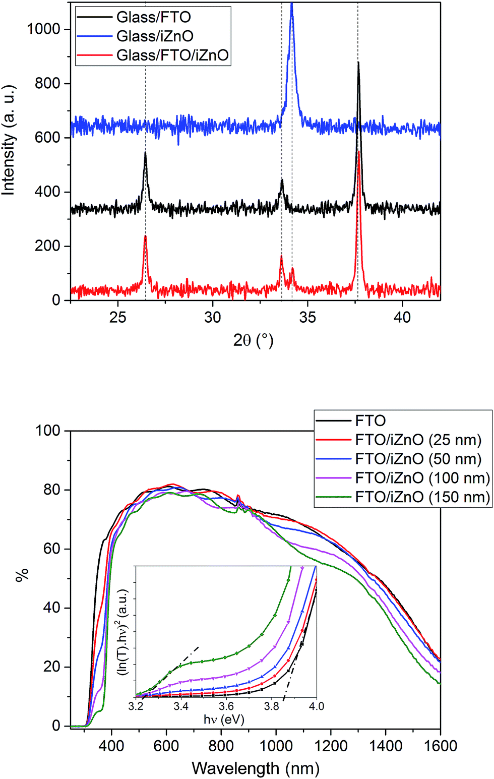
The perovskite solar cell architecture used in this study is the following: glass/fluorine doped tin oxide (FTO)/intrinsic ZnO (i-ZnO)/CH3NH3PbI3/spiro-OMETAD/Au. The FTO/glass substrate used is composed of pyramid shaped grains and shows a highly textured surface. The hole blocking layer (i-ZnO) has to form a conformal film on the substrate surface in order to avoid both the contact between the perovskite layer and the FTO, and between the spiro-OMETAD and the FTO. This requirement is fulfilled by the sputtering method as shown is Fig. 1 which presents the SEM image of the glass/FTO surface with and without i-ZnO covering. At the same time, an insufficiently thin film will increase the series resistance of the device. Thus an optimum value has to be found, therefore intrinsic ZnO layers with thicknesses ranging from 25 to 150 nm have been tested. The structural and optical properties of the sputtered layer have been investigated by X-ray diffraction and transmission spectroscopy (Fig. 2). The ZnO obtained by this method on a flat glass substrate crystallizes in the wurtzite structure and is classically oriented along the c-axis (the (002) peak theoretically appears at 2θ = 34.43°). Despite the high roughness of the FTO substrate this preferential orientation persists as the (002) peaks only appears in the XRD spectrum carried out on the glass/FTO/i-ZnO stack. The transmission spectra show that the substrate is highly transparent in the visible range whatever the i-ZnO thickness. The band gap edge is more and more pronounced as a function of the ZnO thickness and quasi-total absorption is obtained with a thickness of 150 nm for wavelengths lower than 370 nm, showing a good coverage of the FTO surface. The optical bandgap of the ZnO layer has been evaluated at 3.25 eV from the 150 nm thick layer, using the Tauc plot (inset of the Fig. 2) and matches well with the commonly agreed value for an undoped material.
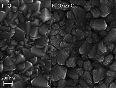 |
| | Fig. 1 SEM image of FTO surface uncovered (left part) and covered by a 80 nm thick ZnO layer (right part). | |
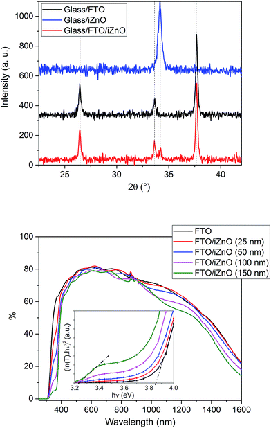 |
| | Fig. 2 Top: X-ray diffractogram of a FTO layer on glass, a 100 nm thick sputtered i-ZnO layer and a glass/FTO/i-ZnO (100 nm) stack. Bottom: UV-vis transmittance spectra of the glass/FTO/i-ZnO substrate as a function of the ZnO thickness. | |
A first batch of CH3NH3PbI3 based solar cells have been built with the different substrates considered. The method used for the growth of the perovskite layer is inspired from the classical two steps wet process which leads to the formation of a homogeneous and covering absorber layer (more details are available in the Experimental part).8 In this section the spin-coating speed for the PbI2 layer and the dipping time in the methyl ammonium iodide (MAI) solution are kept constant and set at 6000 rpm and two minutes respectively. The J–V curves (in dark and under illumination) obtained with the planar architecture (active area of 0.175 cm2) are presented in Fig. 3 and the electrical parameters measured at the reverse scan (from the inverse polarization to the direct polarization) of the best cells are presented in Table 1. A hysteresis in the current response is systematically obtained for this type of architecture and will be discussed below. The shape of diode characteristics obtained in dark is strongly linked to the thickness of the sputtered ZnO layer. Indeed the curves are shifted towards higher potential as the thickness is increased. This effect could be related to the decrease of the dark current that is likely due to a reduction of the carrier recombination at the interface between the perovskite and the n-type contact. The impact of the intrinsic layer is also clearly visible on the electrical parameters measured under illumination. The cells with no blocking layer or with the thinnest ones (25 nm and 50 nm) show very low short current densities leading to low device performances. As no important shunt is observed on the J–V curves measured in dark, this can be attributed to recombination between electrons and holes at the FTO/perovskite interface. The increase of the short circuit current together with that of the open circuit voltage with the i-ZnO thickness seems to confirm that this layer efficiently blocks the holes and passivates the FTO surface. However a too thick i-ZnO layer (150 nm) increases the series resistance affecting dramatically the fill factor and consequently the performance of the solar cell. An optimum has been found near 100 nm with a PCE of 8.2% with a JSC of 12.3 mA cm−2, a VOC of 1.02 V and a FF of 62.5% (Table 2).
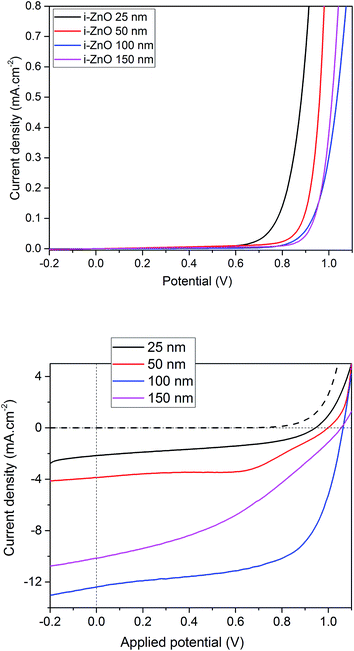 |
| | Fig. 3 J–V curves obtained for a FTO/i-ZnO/CH3NH3PbI3/spiro-OMETAD/Au stack with different i-ZnO thicknesses layers, in dark (top) and under illumination (bottom). | |
Table 1 Photovoltaic parameters of the best perovskite solar cells obtained with different i-ZnO layer thicknesses with a spin-coating speed for the PbI2 layer deposition and a dipping time in the methyl ammonium iodide (MAI) solution set at 6000 rpm and two minutes respectively
| i-ZnO thickness (nm) |
VOC (V) |
JSC (mA cm−2) |
FF (%) |
PCE (%) |
| 25 |
0.94 |
2.15 |
42.7 |
0.8 |
| 50 |
1.01 |
3.8 |
55.8 |
2.1 |
| 100 |
1.06 |
12.3 |
62.5 |
8.2 |
| 150 |
1.06 |
10.1 |
38.2 |
4.1 |
Table 2 Photovoltaic parameters of the best solar cell obtained in this study (spin coating speed of 6000 rpm, and a dipping time of 5 min)
| Bias |
Rotating speed |
Dipping time |
VOC (V) |
JSC (mA cm−2) |
FF (%) |
PCE (%) |
| Reverse |
6000 rpm |
5 min |
1.03 |
19.5 |
70.8 |
14.2 |
| Forward |
1.03 |
18.4 |
43.2 |
8.1 |
Optimization of the perovskite layer
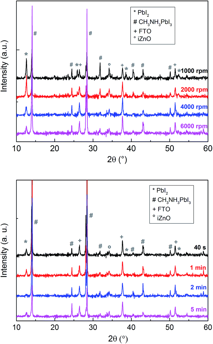
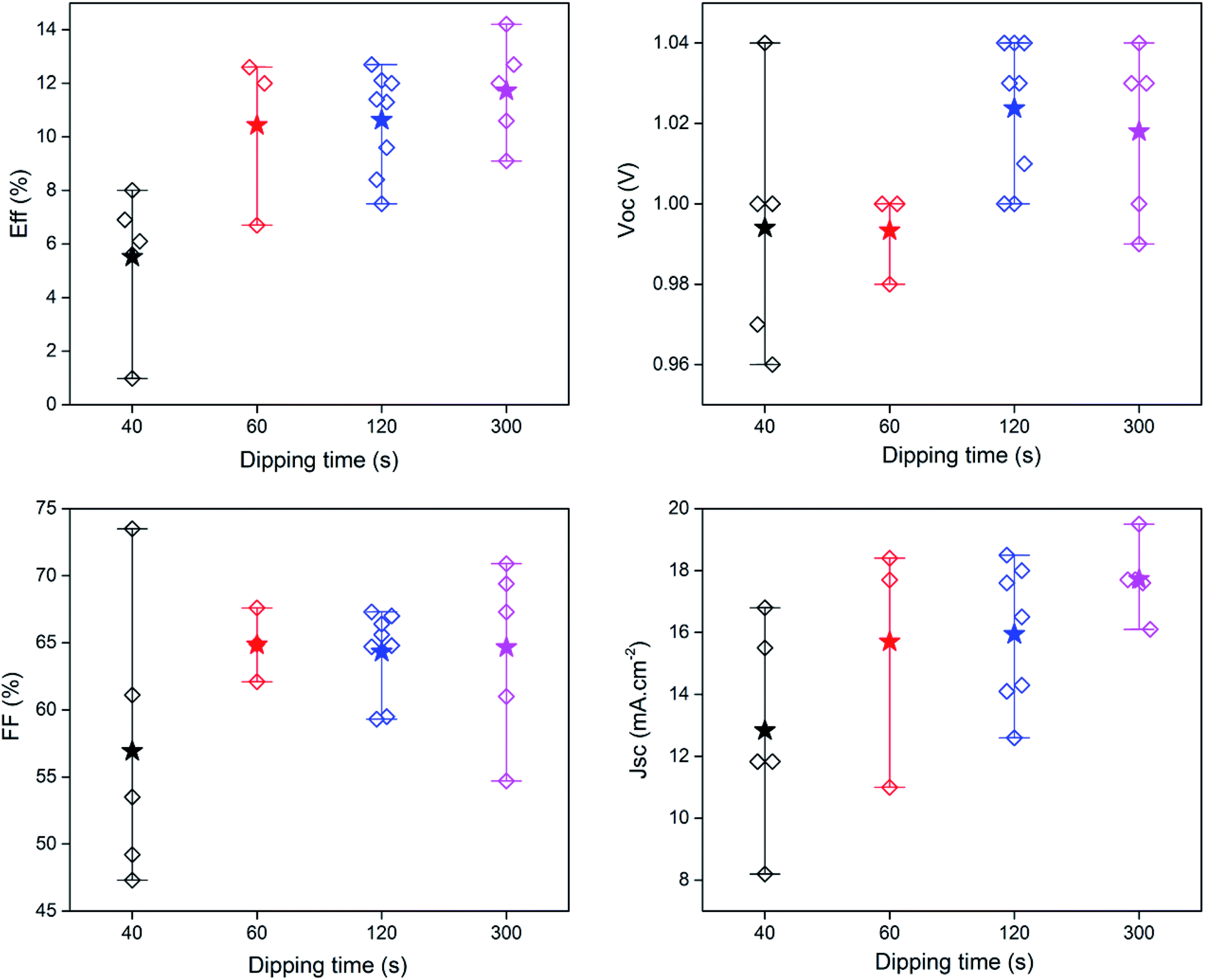
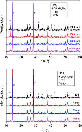
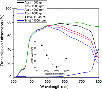
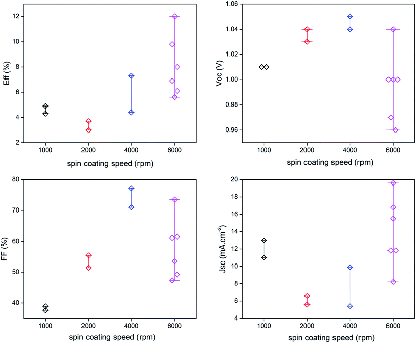
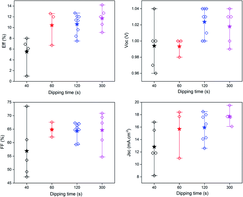
The growth parameters of the perovskite layer have been optimized in order to adapt its deposition process on the 100 nm thick sputtered i-ZnO used as hole blocking layer. As already mentioned, a wet two steps method is applied which consists first in the deposition of a PbI2 layer by spin-coating followed by a dipping in a MAI solution. The influence of the spin-coating speed and the dipping time have been studied keeping the concentration of the precursor constant. It should be noticed that the deposition of the perovskite layer has been carried out, outside gloves box, without any control of the environmental conditions. A fine control of the PbI2 thin film properties deposited during the first step is crucial to control the uniformity, morphology and thickness of the resulting perovskite layer. The Fig. 3 shows the morphology of perovskite layers deposited on a sputtered i-ZnO substrate as a function of the spin-coating speed of PbI2 and after a dipping time of 40 s in a MAI solution. As expected, the thicknesses of the PbI2 and perovskite layers monotonically decrease from 710 nm to 85 nm and from 990 nm to 300 nm respectively when the rotation rate is varied from 1000 rpm to 6000 rpm. The surface morphology of the perovskite is also largely impacted as shown in Fig. 4 since the apparent grain size decreases as the spin-coating speed is increased. The XRD spectra of the layers are shown in Fig. 5. For all the conditions, the (001) characteristic peak of the PbI2 phase appears at 2θ = 12.6° beside those of the hybrid perovskite and evidences an incomplete conversion of the precursor layer into perovskite compound. The relative amount of the remaining PbI2 phase in the layer perovskite layer, which can be qualitatively evaluated by the ratio of the XRD peak intensity largely decreases as spin-coating speed increases (and PbI2 layer thickness decreases). The absorption of the layer (calculated from the transmission spectra) obtained in the different conditions and the corresponding maximum current density calculated considering an efficiency of collection of 100% are presented in Fig. 6. In a general manner the absorption is complete between 300 nm and 500 nm, and gradually decreases as the wavelength rises before the gap absorption edge which appears at wavelength around 750 nm. This effect is even more pronounced that the perovskite layer is thin. The corresponding expected short circuit current density ranges from 18.44 mA cm−2 to 16.4 mA cm−2 as the spin coating speed varies from 1000 to 6000 rpm. Moreover, the band gap value of 1.56 eV determined by a Tauc plot from the optical transmission spectrum of a perovskite layer deposited directly on glass is coherent with the literature. The electrical parameters measured under illumination on a cell batch obtained varying the rotation rate are presented in Fig. 7. The performance of the devices appears to be strongly linked to the deposition conditions and is the highest for the thinnest PbI2 layers (obtained with the highest spin-coating speed), notably due to an enhancement of the short circuit current. This trend which is the opposite to that obtained from the optical measurements shows that the absorption is not the main limiting factor of the cell. Moreover the difference observed on the absorption curves can be largely compensated by the light reflection at the gold contact which tends to increase the optical thickness of the perovskite layer. The low efficiencies obtained at the lowest spin-coating speed can be explained by some PbI2 remaining in the layer as the PbI2 precursors layer is too thick. This incomplete transformation can also explain the broad spread of data for cells build in the best conditions showing the poor reproducibility of the synthesis process. In order to further improve the conversion of the PbI2, different dipping durations in the MAI solution are tested. In this case, the spin-coating speed is kept constant and set at 6000 rpm. The dipping was done during 40 s, 1 min, 2 min or 5 min without any stirring of the solution. On the XRD spectra of the layers (Fig. 5) a decrease of the intensity of PbI2 peak at 2θ = 12.6° with the dipping time is observed with a quasi-total vanishing of this phase for a dipping time of 2 minutes. For the longest duration tested (5 minutes in the presented case), the PbI2 characteristic peak reemerges. This shows the existence of an optimum time after which the perovskite formed is decomposed into PbI2 and MAI. This phenomenon has been observed in a reproducible way, but the optimum duration varies from one cell batch to another (from 2 minutes to 5 minutes typically). The optical parameters obtained (in reverse potential sweep) under illumination for a batch of cells built with a perovskite layer obtained varying the dipping conditions presented in Fig. 8 shows the existence of an optimum duration (five minutes for the batch presented). The main impacts of the increase of the dipping time are the improvement of the short circuit current and the fill factor. Moreover the dispersion of the data is reduced particularly for the short circuit current showing a better reliability of the perovskite growth. A maximum efficiency of 14.2% (VOC = 1.03 V, JSC = 19.5 mA cm−2, FF = 70.8%) for a 0.175 cm2 cell active area has been measured applying a reverse potential sweep. The cell performance is much lower as the potential sweep is carried out in the opposite direction. This strong hysteresis phenomenon is commonly observed in the case of flat cell based on compact n-type TiO2 ETL. This electrical behavior is not fully understood and has been attributed to different physical causes such as very large defect density within or near the surface of the material or specifically generated by interface states, or ions migrations.21,22 The hysteresis has also been related to an insufficient charge transfer rate at the perovskite/ETL interface which is particularly marked in the case of a non mesoporous contact geometry.23,24 The measurement of the quantum efficiency of the best cell is shown in Fig. 9. The curve shows a quite constant conversion efficiency (between 63% and 69%) of the incident photons on a large wavelength domain (400–710 nm). The comparison between the transmission curve of the glass/ZnO substrate (which represents the maximum that can be absorbed by the perovskite layer) of the EQE of the complete cell allows determining a collect efficiency ranging from 93 to 100%. A S-shape edge appears in the UV part of the curve and is due to both FTO and ZnO absorption in this energy region. A band gap width of 1.57 eV for the perovskite absorber can be extracted from the EQE drop in the near IR part of the curve. The current obtained by the integration of the EQE curve (18 mA cm−2) is lower than that measured on J–V curve. This noticeable difference, not fully understood so far could partially originates from the large density of defects in the cell structure that impacts the current density when measured under weak incident light flux as in the case of the EQE.
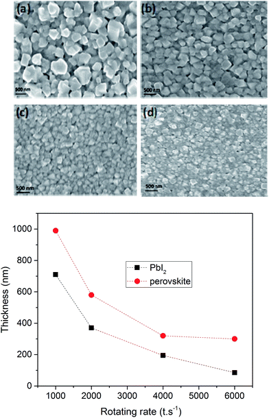 |
| | Fig. 4 Top panel: SEM images of the surface of the perovskite layers obtained from PbI2 films deposited with different spin-coating speed (a) 1000 rpm, (b) 2000 rpm, (c) 4000 rpm and (d) 6000 rpm. Bottom panel: Thicknesses of the PbI2 films and of the corresponding perovskite films as a function of the spin-coating speed. | |
 |
| | Fig. 5 XRD spectra of CH3NH3PbI3 films as a function of the spin-coating speed during the PbI2 deposition (top) and the dipping duration (bottom). | |
 |
| | Fig. 6 UV-vis transmission/absorption of CH3NH3PbI3 films as a function of the spin-coating speed during the PbI2 deposition. Inset: expected current calculated from the absorption spectra considering a 100% collect efficiency. | |
 |
| | Fig. 7 Electrical parameters of the cells measured under illumination on a cell batch obtained varying the rotation rate during the PbI2 layer deposition. | |
 |
| | Fig. 8 Electrical parameters of the cells measured under illumination on a cell batch obtained varying the dipping time in the MAI solution (the stars is the mean value). | |
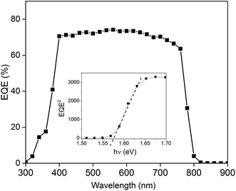 |
| | Fig. 9 Quantum efficiency measurement of the best cell. Inset: determination of the perovskite band gap. | |
Encapsulation/stability
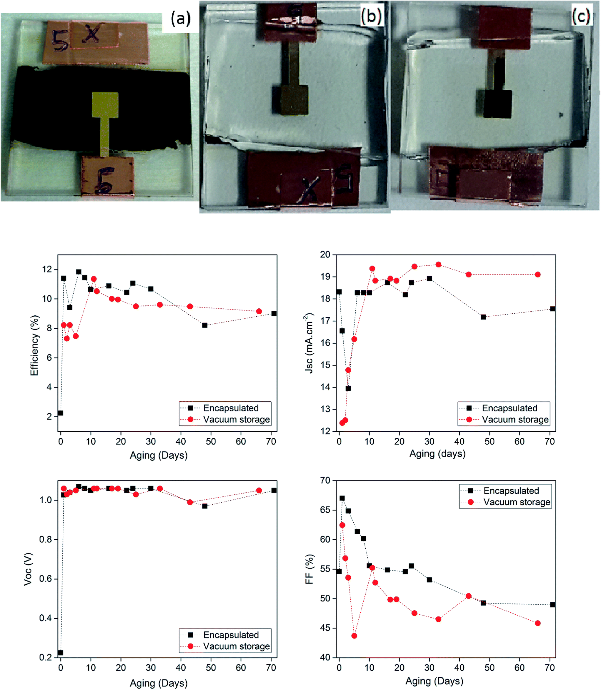
The stability has been studied on two planar perovskite solar cells elaborated in the same conditions. The i-ZnO layer has a thickness of 100 nm, the perovskite was deposited in two steps, with a spin-coating speed of 6000 rpm and a dipping time of 2 min. The performances of the cells (Fig. 10) were regularly measured over 70 days. After the first measurement, carried out just after the device elaboration, both cells have been stored in a vacuum box during one night. In a general manner, during the first hours of storage the performances of the cell largely varies. The short circuit current is particularly affected. This rapid evolution could explain the shift between the JSC calculated from the EQE measurement and that obtained from J–V curve and can be attributed to the evaporation of the residual traces of solvent which remains in the layer after the growth. In the example presented in Fig. 10, and the PCE reaches a maximum value close to 12% after this first step. The following days, the cell no. 1 was stored under vacuum between two cell measurements and the cell no. 2 has been encapsulated with an Araldite glue and stored in ambient atmosphere. Interestingly, the application of the Araldite glue on the cell stack leads to a total discoloration of the cell excluding the zone situated under the gold contact, which acts as a protection layer. The discoloration of the perovskite is not fully understood and may be due to solvent contained in the glue. It leads to a very well defined active layer as shown in Fig. 10. During the following days, both cells evolve in the same way as a function of time with a monotonous decay of the performance mainly due to a decrease of the fill factor ranging from 70% to 50% after 70 days. At contrary, the open circuit voltage and the short circuit current stay remarkably stable. The lowering of the fill factor could be due to a progressive decrease of the conductivity of the spiro-OMETAD, as this compound has often been identified as one of the main sources of instabilities in the cell structure. Degradation of the cells performances may also originate from the migration of iodine ions leading to an oxidation of the metallic contact.25 In this case the fill factor is particularly impacted due an increase of the contact resistance. Moreover the Araldite glue chosen for the encapsulation may not be optimal for this task, and its diffusion can damage the cell. Further experiments are in progress in order to fully understand the degradation mechanism of the cell.
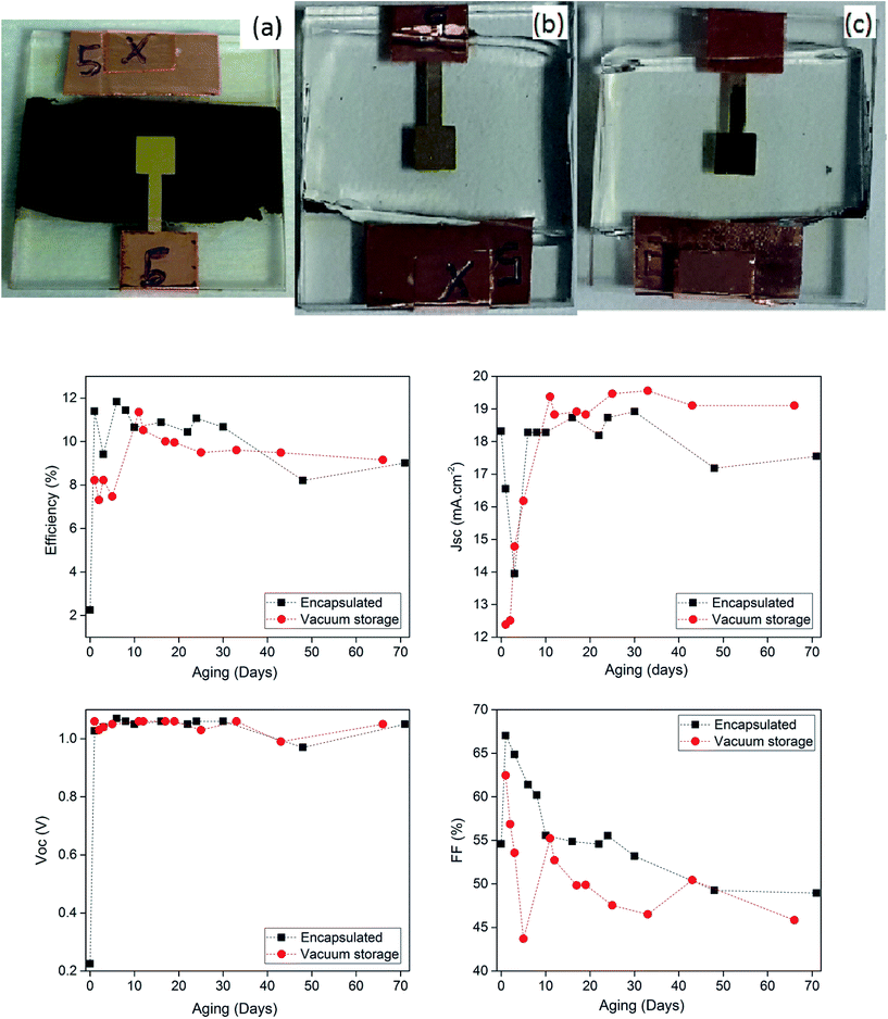 |
| | Fig. 10 Top: Photography of a complete cell before (a) and after encapsulation (b and c). Bottom: Evolution of the photovoltaic electrical parameters of two perovskite planar solar cells stored under vacuum (red points) and under ambient air with encapsulation (black squares). | |
Conclusion
In this paper, sputtered intrinsic zinc oxide (i-ZnO) has been used with success as hole blocking layer in planar perovskite solar cell. i-ZnO is able to ensure the different functions needed to extract the charge carriers generated under illumination. Moreover it allows to efficiently reduce the recombination at the perovskite/FTO interface. Efficiency up to 14.2% has been obtained optimizing both the i-ZnO layer thickness and the perovskite deposition process. However, the perovskite solar cells obtained in this study show a strong hysteresis phenomenon depending on the J–V scanning direction. Further experiments are in progress to suppress this effect like modification of the interface or the use of additional rough layer onto the i-ZnO layer. Finally the VOC and JSC stay remarkably constant over two months after encapsulation or with a storage in vacuum conditions. At contrary a decrease of fill factor, which may be related to a degradation of the metallic contact, is observed and affects the overall performance of the cell.
Experimental section
First, a 100 nm compact layer of ZnO was sputtered on a transparent conducting fluorine-doped SnO2-coated glass substrate (FTO). The FTO was ultrasonically pre-cleaned sequentially in detergent (Hellmanex in water), deionized water, ethanol and acetone and finally dried under a flow of N2. The compact ZnO layer was first heated at 150 °C during 30 min to improve the wettability and then at 70 °C before the deposition. Perovskite was then deposited in wet two steps as described in previous reports.8 PbI2 (Alfa Aesar, 99.99% purity) is spin-coated onto the ZnO from a solution 1 mol L−1 PbI2 in dimethylformamide (DMF) (Merck) during 30 s at different spin-coating speed and then heated at 70 °C during 50 min to remove the solvent. CH3NH3PbI3 is formed by dipping the PbI2 film into a solution of MAI in 2-propanol (10 mg mL−1). The perovskite was then washed in 2-propanol to remove the excess of MAI and heated at 70 °C during 50 min to remove the solvent. The thickness of the different layers have been measured by calibrated X-ray fluorescence and confirmed by contact profilometry. The Hole Transportation Material (HTM) was deposited on the perovskite layer by spin-coating at 4000 rpm during 30 s. The HTM used is spiro-OMETAD (Sigma Aldrich) diluted in chlorobenzene (72 mg mL−1) with an addition of 28.5 μL of 4-tBP (Sigma-Aldrich) and 17.5 μL of Li–TFSI solution (520 mg Li–TFSI in 1 mL acetonitrile, Sigma-Aldrich, 99.8%).
Finally, a 100 nm thick gold layer was deposited by thermal evaporation at a base pressure of 5 × 10⁻⁷ mbar using a mask giving an effective active area of 0.175 cm2. All device fabrication steps were carried out under ambient conditions.
The current density–voltage (J–V) curves were measured by a solar simulator (Sol 3A class AAA) with a potentiostat (Keithley 2635) under illumination of 1 sun (100 mW cm−2) AM 1.5G.
References
- H.-S. Kim, C.-R. Lee, J.-H. Im, K.-B. Lee, T. Moehl, A. Marchioro, S.-J. Moon, R. Humphry-Baker, J.-H. Yum, J. E. Moser, M. Grätzel and N.-G. Park, Sci. Rep., 2012, 2, 1 Search PubMed.
- A. Kojima, K. Teshima, Y. Shirai and T. Miyasaka, J. Am. Chem. Soc., 2009, 131, 6050 CrossRef CAS PubMed.
- M. Saliba, T. Matsui, J.-Y. Seo, K. Domanski, J.-P. Correa-Baena, K. N. Mohammad, S. M. Zakeeruddin, W. Tress, A. Abate, A. Hagfeldt and M. Grätzel, Energy Environ. Sci., 2016, 9, 1989 CAS.
- C. Tao, S. Neutzner, L. Colella, S. Marras, A. R. Srimath Kandada, M. Gandini, M. D. Bastiani, G. Pace, L. Manna, M. Caironi, C. Bertarelli and A. Petrozza, Energy Environ. Sci., 2015, 8, 2365 CAS.
- M. M. Lee, J. Teuscher, T. Miyasaka, T. N. Murakami and H. J. Snaith, Science, 2012, 338, 643 CrossRef CAS PubMed.
- W. S. Yang, J. H. Noh, N. J. Jeon, Y. C. Kim, S. Ryu, J. Seo and S. I. Seok, Science, 2015, 348, 1234 CrossRef CAS PubMed.
- N. Ahn, D.-Y. Son, I.-H. Jang, S. M. Kang, M. Choi and N.-G. Park, J. Am. Chem. Soc., 2015, 137, 8696 CrossRef CAS PubMed.
- http://www.nrel.gov/ncpv/images/efficiency_chart.jpg.
- S. D. Stranks, G. E. Eperon, G. Grancini, C. Menelaou, M. J. P. Alcocer, T. Leijtens, L. M. Herz, A. Petrozza and H. J. Snaith, Science, 2013, 342, 341 CrossRef CAS PubMed.
- Q. Dong, Y. Fang, Y. Shao, P. Mulligan, J. Qiu, L. Cao and J. Huang, Science, 2015, 347, 967 CrossRef CAS PubMed.
- J. Burschka, N. Pellet, S.-J. Moon, R. Humphry-Baker, P. Gao, M. K. Nazeeruddin and M. Grätzel, Nature, 2013, 499, 316 CrossRef CAS PubMed.
- Z. Xiao, C. Bi, Y. Shao, Q. Dong, Q. Wang, Y. Yuan, C. Wang, Y. Gao and J. Huang, Energy Environ. Sci., 2014, 7, 2619 CAS.
- T. Hakamata, K. Shimamura, F. Shimojo, R. K. Kalia, A. Nakano and P. Vashishta, Sci. Rep., 2016, 6, 19599 CrossRef CAS PubMed.
- G. Xing, N. Mathews, S. Sun, S. S. Lim, Y. M. Lam, M. Gratzel, S. Mhaisalkar and T. C. Sum, Science, 2013, 342, 344 CrossRef CAS PubMed.
- D. Liu and T. L. Kelly, Nat. Photonics, 2013, 8, 133 CrossRef.
- D.-Y. Son, K.-H. Bae, H.-S. Kim and N.-G. Park, J. Phys. Chem. C, 2015, 119, 10321 CAS.
- D.-Y. Son, J.-H. Im, H.-S. Kim and N.-G. Park, J. Phys. Chem. C, 2014, 118, 16567 CAS.
- J. Zhang, P. Barboux and T. Pauporté, Adv. Energy Mater., 2014, 4, 1400932 CrossRef.
- J. Zhang and T. Pauporté, J. Phys. Chem. C, 2015, 119, 14919 CAS.
- Ü. Özgür, Y. I. Alivov, C. Liu, A. Teke, M. A. Reshchikov, S. Doğan, V. Avrutin, S.-J. Cho and H. Morkoç, J. Appl. Phys., 2005, 98, 041301 CrossRef.
- J. H. Heo, M. S. You, M. H. Chang, W. Yin, T. K. Ahn, S.-J. Lee, S.-J. Sung, D. H. Kim and S. H. Im, Nano Energy, 2015, 15, 530 CrossRef CAS.
- E. Edri, S. Kirmayer, A. Henning, S. Mukhopadhyay, K. Gartsman, Y. Rosenwaks, G. Hodes and D. Cahen, Nano Lett., 2014, 14, 1000 CrossRef CAS PubMed.
- G. Xing, B. Wu, S. Chen, J. Chua, N. Yantara, S. Mhaisalkar, N. Mathews and T. C. Sum, Small, 2015, 11, 3606 CrossRef CAS PubMed.
- H. J. Snaith, A. Abate, J. M. Ball, G. E. Eperon, T. Leijtens, N. K. Noel, S. D. Stranks, J. T.-W. Wang, K. Wojciechowski and W. Zhang, J. Phys. Chem. Lett., 2014, 5, 1511 CrossRef CAS PubMed.
- H. Back, G. Kim, J. Kim, J. Kong, T. K. Kim, H. Kang, H. Kim, J. Lee, S. Lee and K. Lee, Energy Environ. Sci., 2016, 9, 1258 CAS.
|
| This journal is © The Royal Society of Chemistry 2016 |
Click here to see how this site uses Cookies. View our privacy policy here.