Low-voltage carbon films deposition by electro-exfoliation of graphite into graphene oxide

Alan M. P. Sakitaa, Marco A. G. Valente Jr.a, Rodrigo Della Noceb, Cecílio S. Fugivaraa, Marina Magnania and Assis V. Benedetti*a
aInstituto de Química, UNESP-Universidade Estadual Paulista, 14800-900 Araraquara, Brazil. E-mail: benedeti@iq.unesp.br
bCentro de Química Estrutural-CQE, Department of Chemical Engineering, Instituto Superior Técnico, Lisbon, Portugal

Received 26th June 2016 , Accepted 29th August 2016

First published on 30th August 2016


Abstract

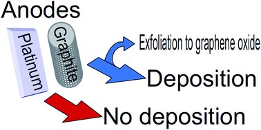
Low-voltage carbon films deposition by electro-exfoliation of graphite into graphene oxide is reported. By simply employing two different anodes, Pt or graphite, it is demonstrated that the carbon film deposition takes place by the graphite electro-exfoliation and not by the carbonic molecules from the electrolyte as has been frequently reported. By means of Raman spectroscopy, scanning electron microscopy (SEM), cyclic voltammetry (CV), X-ray diffractometry (XRD), atomic force microscopy (AFM), and dynamic light scattering (DLS), graphene oxide is successfully characterized. In addition, this electro-exfoliation process may be an alternative green route for the production of graphene oxide.


1. Introduction

Carbon thin films have attracted great research interest because they show good electrical, mechanic, and chemical properties, which makes this material promising for many applications including biomaterial coatings, photovoltaics, and electronic devices.1–3 Recently, several papers have demonstrated the production of diamond-like carbon (DLC) by electrodeposition,4–10 which presents better cost-effectiveness than typically physical deposition methods such as PVD, CVD, and PECVD.11,12 It has been extensively reported that the carbon source in DLC electrodeposition is the solution component.4,5,10 However, most of these works has used graphite as anode which might be a carbon source too. For instance, Roy et al.4 reported the DLC deposition at high voltage using acetic acid aqueous solution as carbon source and described the growth of DLC by the polarization of acetic acid followed by ionization of the organic molecule under high electrical field. DLC electrodeposition on Si(111) at low voltage was investigated by Sreejith et al.5 that showed the possibility of depositing DLC from ethanol solutions in the range of 80–300 V. Recently, Zhang et al.10 depicted the DLC deposition in chloroacetic acid solution using a graphite anode and by applying 3 V. The Raman spectra of the deposit revealed DLC characteristic bands, however, the electrolyte was considered as the carbon source. DLC deposition has been performed using non-carbon-based anodes, but in these cases, either high voltages13–18 or low temperatures19,20 are always employed (see Table S1 on ESI). In the case of using low temperatures, the carbon film deposition takes place by oxidation of the electrolyte.

Nowadays, with increasing researches employing graphene products, one of the current concerns is about environmental friendly synthesis which can be prepared by several methods.21 One of the most used routes for graphene oxide production is based on the Hummers method,22 where a large content of residues is generated and an extensive wash is needed for the graphene oxide purification. New non-aggressive methods have been studied to avoid the residues generation, and the electro-exfoliation has revealed to be a promising way to prepare large-scale, homogeneous, and good quality graphene products.23,24 However, the current electro-exfoliation methods are still dependent on a high post-treatment of the graphene-containing solution for the electrolyte elimination.23,25–27

Herein, we report on the low-voltage carbon films deposition by electro-exfoliation of graphite into graphene oxide. By simply employing two different anodes, Pt or graphite, we demonstrate that the carbon film deposition takes place by the graphite electro-exfoliation and not by the carbonic molecules from the electrolyte as has been frequently reported. By means of Raman spectroscopy, scanning electron microscopy (SEM), cyclic voltammetry (CV), atomic force microscopy (AFM), and dynamic light scattering (DLS), graphene oxide is successfully characterized. Moreover, this electro-exfoliation process may be an alternative green route for the production of graphene oxide.

2. Experimental details

Ti–6Al–4V alloy was utilized as substrate (cathode) which was polished with SiC 1200 mesh emery paper. Prior to each deposition experiment, the substrate was immersed in boiling 10% oxalic acid solution for 10 minutes. The electrolysis to obtain the carbon films deposition was performed for 24 hours and the details are described in Table 1. The electrolyte was composed of 1% formic acid aqueous solution (1% FA) as previously described for DLC electrodeposition.28
Table 1 Experimental conditions used to produce the carbon thin films by applying 8 V
Experiment Cathode Anode Solution
a The solution obtained at the end of D1 experiment was centrifuged and used in D3 experiment.
D1 Ti–6Al–4V Graphite FA 1%
D2 Ti–6Al–4V Pt FA 1%
D3 Ti–6Al–4V Pt D1 after electrolysisa


A graphite rod (Alfa Aesar 99.997%) or a platinum sheet were used as anode being placed at 7 mm of distance from the cathode.

The surface morphology and elemental composition of the cathodes were investigated by energy dispersive X-ray spectrometer (EDS) coupled to SEM, using a JEOL JSM-7500F field emission electron microscope (FEG) and a NORAN System 6. The films were also characterized by Raman spectroscopy using a μ-Raman Horiba Jobin Yvon LabRAM HR800 instrument equipped with a laser operating at 632.81 nm, and by infrared spectroscopy employing a FTIR spectrophotometer Frontier Dual Range – PerkinElmer coupled to ATR accessory. Cyclic voltammograms were recorded in 0.5 M H2SO4 solution at 20 mV s−1 and 25 °C using a Bio-Logic VSP potentiostat/galvanostat controlled by EC-LAB 10.44 software.

After electrolysis, the solution D1 was characterized by AFM (Agilent 5500 AFM). For this experiment, the electrolyzed solution D1 was diluted in a proportion of 1[thin space (1/6-em)]:[thin space (1/6-em)]10 in water. The resultant solution was dropped in a single-crystal Si(111) and deposited by spin coating ​(Spincoater MicroTube A1v1.1.2) at 3000 rpm during 40 seconds. The silicon substrate was dried at 60 °C during 24 hours. The diluted solution D1 (1[thin space (1/6-em)]:[thin space (1/6-em)]10) was also analyzed by DLS and Zeta titration analyses using a Zetasizer Nanoseries ZSNano ZEN3600 (Malvern Instruments). Transmission electron microscopy (TEM) was carried out at the Brazilian Nanotechnology National Laboratory (LNNano), using a JEOL JEM 3010 microscope operated at 300 kV (1.7 Å resolution). XRD analysis was performed using a D5000 Siemens diffractometer, and UV-Vis spectrometry was conducted at a Hitachi U-2000 spectrometer.

3. Results and discussion

Graphene, reduced graphene oxide (rGO), and graphene oxide (GO) when in solution and at high concentration reveal a dark color.23,29,30 After 24 hours electrolysis, the solution from the experiment D1 showed a dark brown color, while the solution from the experiment D2 was colorless (Scheme 1 at ESI), indicating no effect of the electrolysis on the solution color when a platinum anode was used. Additionally, the graphite anode used in the experiment D1 showed erosion on the surface, demonstrating carbon exfoliation, and a little amount of carbon powder was observed at the bottom of the electrochemical cell. Optical micrographs revealed a cloudy Ti alloy surface after the experiment D1 compared to the bare surface initially observed, which was attributed to the carbon film deposition. Other important indicative of the carbon film deposition was the brownish color of the cathode surface at the end of the experiment, the same color as reported in literature.31–37 In the experiment D2, the cathode surface showed similar behavior to the bare titanium alloy, indicating no surface modification.

The yield was estimated to be 20% (mGO/(mi,anodemf,anode)), where mi and mf are the initial and final mass of anode; the cathode products were not considered. Najafabadi and Gyenge25 obtained graphene by graphite electro-exfoliation with a yield of 15% estimated on the change of the anode volume and considering that all the lost volume was converted into graphene. The chemical Hummer's method can reach values of yield up to 95% (ref. 38) but several drawbacks are involved when scale-up is considered due to the large volume of hot solutions and strong oxidants reactants handled, and post treatment of the products is needed. It is important to note that our work focuses on carbon films formation from graphite electro-exfoliation at low electrical field and room temperature. Additionally, it demonstrates that, under the proposed conditions, carbon films are not produced using platinum as anode (see Table S1 for more details).

Fig. 1 shows the Raman spectra of the cathode surfaces after electrolysis. The spectra obtained after experiments D1 and D3 depicted two peaks at 1334 and 1605 cm−1 corresponding to D and G bands, respectively, which are characteristic of materials with sp2 and sp3 carbon hybridized orbitals.39 These bands were not detected in the spectrum of the D2 experiment cathode, revealing that carbon film was not deposited. Recently, Raman spectra similar to that obtained after experiments D1 and D3 were related to DLC electroformed.10 The powders spectra, resulting from drying the solutions (DS) of D1 and D3 experiments (curve DS in Fig. 1), were similar to those of the solutions. This supports the hypothesis that the carbon source is originated from the graphite anode and not from the formic acid solution. Hence, it can be inferred that graphene oxide was obtained from the graphite anode by electro-exfoliation. The weak 2D band observed at 2675 cm−1 (Fig. S1) is related to single layered GO. This result is in agreement with the particle's size measured by AFM.


image file: c6ra16502h-f1.tif
Fig. 1 Raman spectra of the cathode surfaces obtained from the Table 1 experiments and dried solution D1 after electrolysis.

Fig. 2, S2 and S3 (see ESI) display the infrared spectra (a) and zoomed region (b) between 2000 and 1200 cm−1 of the cathodes surface prepared under the conditions listed in Table 1. For samples D1 and D3 three peaks at about 2854 cm−1 (sp3-CH2 symmetric vibration), 2922 cm−1 (sp3-CH2 symmetric vibration) and 2966 cm−1 (sp3-CH3 asymmetric vibrations) are observed, which can be assigned to the diamond-like structure present in the formed film.10,31 Moreover, Fig. 2B depicts at least three peaks comprising lengths lower than 1800 cm−1, which can be associated to C[double bond, length as m-dash]O and C–O–C stretching modes.40 For the dried solutions powder, the peak ca. 1025 cm−1 was attributed to C–O from epoxides while this peak was not observed for D1 and D3 experiments due to the electrochemical reduction of C–O groups. The two peaks at 1450 (weak intensity) and 1365 cm−1 (medium intensity) can be attributed to C–H bending of the carbon films41 prepared in D1 and D3 experiments. The cathode surface prepared in D2 experiment showed an intense broad peak about 850 cm−1 which is typical of TiO2 materials.42,43


image file: c6ra16502h-f2.tif
Fig. 2 ATR-FTIR spectra of the cathode surface prepared in experiments described in Table 1. (A) 4000 to 500 cm−1 and (B) 2000 to 1200 cm−1.

In order to know the cathodes morphology, SEM was performed after the electrodeposition process as illustrated in Fig. 3. The D1 surface morphology (Fig. 3B) revealed furrow-like structure and small nodules all over the surface while large number of nodules on D3 surface was noticed (Fig. 3C). The nodules observed in Fig. 3C, where no carbon film was detected (Fig. 1 and 2), were attributed to the formation of a phase with higher concentration of Al and V (Fig. S4). On the other hand, platinum anode showed no carbon film deposition in spite of formic acid presence in the electrolyte. Therefore, at low potentials (<8 V), this result indicates that graphite is the carbon source, and does not support the formation of carbon film from formic acid,28 acetic acid,6,28,44–47 chloroacetic acid,10 or ethanol,5,11 as previously reported.8,48,49 In fact, Grill50 described the necessity of high energetic procedures for deposition of DLC films, which indeed showed to be difficult by electrochemical means due to solvation, diffusion, and side reactions.


image file: c6ra16502h-f3.tif
Fig. 3 SEM images of the samples obtained under the conditions described in Table 1. (A) Bare cathode, (B) D1, (C) D2 and (D) D3.

CV was employed in order to evaluate possible changes in the cathodes surface mainly with respect to their surface area. Fig. 4 shows the cyclic voltammograms of the cathodes surface recorded in 0.5 M sulfuric acid electrolyte. In the first cycle, the CV of Ti–6Al–4V alloy (Fig. 4A) revealed two oxidation peaks, which were related to titanium oxide growth.51,52 The subsequent cycles showed a capacitive behavior with a very low current density owing to slow rate of oxide growth. When Pt was used as anode in the D2 experiment, the current density for the oxide growth on Ti alloy shifted to more positive potentials, which could be linked to richer Al–V nodules formation. On the positive potential scanning, D1 presented a low current peak at ca. 0.85 V related to titanium oxide growth, while for D2 a higher current peak was observed, which in fact revealed the surface coverage by a carbon film. For D1 and D3 experiments, the CVs showed a current peak at −0.175 V attributed to the reduction of C[double bond, length as m-dash]O and C–O–C groups from the surface53 (Fig. 2B), which decreased in the second and third cycles. Thus, CV revealed to be a good technique for the characterization of carbon films due to the reduction of oxygenated groups. DLC films present a great number of sp3 C–C bonds, and this property in general hinders the electrical conduction of the film. Some articles have described the DLC chemical structure by means of Raman spectroscopy which is a helpful tool to the surface characterization, but cyclic voltammetry can disclose the electrical properties and also study the changes in its surface area. At this point, this work shows that samples D1 and D3 possess similar electrochemical behavior to each other. The low current density related to the titanium oxide growth in CV of D1 and D3 are a strong indication in which the surface was covered with a layer of carbon film that acts as a physical barrier. The surface coverage is observed in SEM (Fig. S6), where was possible to see pitted regions in bare Ti alloy and in D2 surface, while for D1 and D3 no pits were observed. The cathodic peak ca. −0.175 V in the samples D1 and D3 was another significant sign of the similarity between the samples. On the other hand, the experiment D2 revealed a current peak attributed to oxide growth, which indicates no surface coverage at all.


image file: c6ra16502h-f4.tif
Fig. 4 Cyclic voltammograms of cathodes prepared as described in Table 1, obtained in 0.5 M H2SO4 at 20 mV s−1 and 25 °C. (A) Bare titanium alloy, (B) after D1 experiment, (C) after D2 experiment and (D) after D3 experiment.

The as-prepared product from the graphite electro-exfoliation is mainly GO while when the dried solution is analyzed rGO is detected. In order to evaluate if the prepared solution is composed by GO or rGO, a test adding ascorbic acid (AA) to the D1 solution has been done. This indicates that the reduction of the initial product has occurred and then, further experiments have been performed to support this hypothesis. Therefore, the graphene oxide formation is indirectly demonstrated by reducing it to rGO, which exhibits a darker color (Fig. S7). UV-Vis absorption spectrum (Fig. S8) for the as-prepared solution (Fig. S7 left, without AA addition) shows a peak at 204 nm related to the π–π* transition of the C[double bond, length as m-dash]C bond, which is characteristic of the GO formation since the peak is located in a region lower than 250 nm. Thus, it can be inferred that the as-prepared solution is mainly composed by GO.54 On the other hand, the dried solution analyzed by AFM, HR-TEM, and XRD shows rGO further reduced as a consequence of the heating and the presence of formic acid.55

To confirm the presence of graphene oxide, the solution after D1 electrolysis was also analyzed by AFM (Fig. 5 and S9) and DLS (Fig. 8). The AFM analysis reveals particles with average diameter of 70 nm and a thickness ranging from 0.35 to 3 nm, which are in agreement with a single and layered graphene oxide.53,56 The size distribution obtained by DLS shows a high population in 30 nm diameter size, featuring a nanosized graphene oxide.40 The difference between the particles size obtained by AFM and DLS reveals the dependence of conformation of GO by the chemical environment. Therefore, AFM and DLS evidence that the graphite anode plays an important role on the deposition of carbon films depicting its exfoliation into nanographene oxide.


image file: c6ra16502h-f5.tif
Fig. 5 AFM image of D1 electrolyzed solution placed on the top of Si(111) surface.

image file: c6ra16502h-f6.tif
Fig. 6 HR-TEM image of rGO: (A) insert shows the interlayer distance, (B) aggregated rGO.

image file: c6ra16502h-f7.tif
Fig. 7 XRD pattern of the dried solution D1 showing the rGO formation.

image file: c6ra16502h-f8.tif
Fig. 8 DLS analysis of D1 solution after electrolysis. The solution was centrifuged at 10[thin space (1/6-em)]000 rpm during 10 minutes and posterior dilution to 1[thin space (1/6-em)]:[thin space (1/6-em)]10 with water.

HR-TEM images show a good crystallinity of rGO, with an interlayer distance about 0.3 nm, in good agreement with XRD data as well as other reported works.57–60 This information is found in Fig. 6A and B depicts an aggregated of rGO 80 nm sized, similar to that previously observed by AFM (Fig. 5).

The XRD pattern of the dried solution (Fig. 7) reveals a broad peak at 23.99° related to (002) plane with a lattice spacing of 0.375 nm, indicating the formation of rGO, which is expected due to the chemically reduction of GO caused by formic acid. This interlayer spacing value is in accordance with HR-TEM results that shows an average value of 0.3 nm; these values are similar to those previously reported for rGO.53,57,59

The zeta potential (ζ) measurements of electro-exfoliated graphene oxide as pH function are shown in Fig. 9. It is seen that at pH near 3.8 (formic acid 1% v/v) was observed negative potential about −20 mV. Increasing the pH, ζ decreases as a consequence of the negative charge on the graphene oxide functional groups which were observed by FT-IR (Fig. 2). The negative potential observed at acid solution with pH < 3 is a result of the ionization of the carboxylic acid and phenolic groups present in GO.61 Although the deposition of graphene oxide upon the cathode was observed by several methods employed in this work, the current efficiency for the deposition was very low due to the intense gas evolution on the electrodes that allows the graphite exfoliation and the highly negative charge observed by zeta titration. The values of ζ observed in the as-prepared graphene oxide solution shows to be promising for the anodic electrophoretic deposition of graphene oxide as earlier reported.62


image file: c6ra16502h-f9.tif
Fig. 9 Zeta potential (ζ) of electro-exfoliated graphene oxide as a function of pH. The solution obtained after 24 hours electrolysis was diluted 10 times plus the addition of 1 mM NaCl.

The methodology employed for the graphite electro-exfoliation in this work shows a green way to exfoliate graphite compared to the usually ones reported in literature. In general, those routes reveal the necessity of copious amounts of water to wash the exfoliated product unlike the one herein described, where it is only needed to dry the whole solution to directly obtain reduced graphene oxide.

4. Conclusions

In conclusion, we have demonstrated the low-voltage carbon films deposition by electro-exfoliation of graphite into graphene oxide. Under the proposed experimental conditions, carbon is provided by graphite anode instead of carbonic molecules from the electrolyte containing formic acid. Furthermore, this electro-exfoliation process may be an alternative green route for the production of graphene oxide.

Acknowledgements

The authors gratefully acknowledge financial support and scholarships provided by Brazilian funding agencies CNPq (AMPS proc. no. 141257/2014-8) and CAPES (MAGV). RDN would like to acknowledge FCT for financial support under the project PEst-OE/QUI/UI0100/2013. The authors also thank GFQM, LMF, LAMMC, and LMA-IQ for Raman, FTIR-ATR, FEG-SEM, XRD, DLS and AFM analyses and LNNano (CNPEM) for the TEM images.

References

  1. A. A. Balandin, Nat. Mater., 2011, 10, 569–581 CrossRef CAS PubMed.
  2. A. H. Lettington, Carbon, 1998, 36, 555–560 CrossRef CAS.
  3. C. A. Charitidis, Int. J. Refract. Met. Hard Mater., 2010, 28, 51–70 CrossRef CAS.
  4. R. K. Roy, B. Deb, B. Bhattacharjee and A. K. Pal, Thin Solid Films, 2002, 422, 92–97 CrossRef CAS.
  5. K. Sreejith, J. Nuwad and C. G. S. Pillai, Appl. Surf. Sci., 2005, 252, 296–302 CrossRef CAS.
  6. R. Paul, S. Dalui, S. N. Das, R. Bhar and A. K. Pal, Appl. Surf. Sci., 2008, 255, 1705–1711 CrossRef CAS.
  7. T. Falcade, T. Eduardo, O. Gomes, A. Luis, M. Vargas, R. Hübler, I. Lourdes and C. De Fraga, Appl. Surf. Sci., 2012, 263, 18–24 CrossRef CAS.
  8. B. Ghosh, D. Ghosh, A. Ghosh, S. Hussain, R. Bhar and A. K. Pal, Mater. Sci. Semicond. Process., 2014, 25, 130–136 CrossRef CAS.
  9. S. Wan, H. Hu, G. Chen and J. Zhang, Electrochem. Commun., 2008, 10, 461–465 CrossRef CAS.
  10. Q. Zhang, Y. Wang, W. Wang, N. Mitsuzak and Z. Chen, Electrochem. Commun., 2016, 63, 22–25 CrossRef CAS.
  11. H. Pang, X. Wang, G. Zhang, H. Chen, G. Lv and S. Yang, Appl. Surf. Sci., 2010, 256, 6403–6407 CrossRef CAS.
  12. C. Donnet, Surf. Coat. Technol., 1998, 100–101, 180–186 CrossRef CAS.
  13. H. S. Zhu, J. T. Jiu, Q. Fu, H. Wang and C. B. Cao, J. Mater. Sci., 2003, 38, 141–145 CrossRef CAS.
  14. Z. Sun, Y. Sun and X. Wang, Chem. Phys. Lett., 2000, 318, 471–475 CrossRef CAS.
  15. X. Kong, S. Wang, H. Zhao and Y. He, Thin Solid Films, 2010, 518, 4211–4214 CrossRef CAS.
  16. Y. Li, G. Zhang, X. Hou and D. Deng, Appl. Surf. Sci., 2012, 258, 6527–6530 CrossRef CAS.
  17. J. Tsukada, H. Zanin, L. C. a. Barbosa, G. a. da Silva, H. J. Ceragioli, A. C. Peterlevitz, R. F. Teofilo and V. Baranauskas, J. Electrochem. Soc., 2012, 159, D159–D161 CrossRef CAS.
  18. H. Wang and M. Yoshimura, Chem. Phys. Lett., 2001, 348, 7–10 CrossRef CAS.
  19. V. P. Novikov and V. P. Dymont, Appl. Phys. Lett., 1997, 70, 200 CrossRef CAS.
  20. A. M. Chen, C. Pingsuthiwong and T. D. Golden, J. Mater. Res., 2003, 18, 1561–1565 CrossRef CAS.
  21. Y. Zhu, S. Murali, W. Cai, X. Li, J. W. Suk, J. R. Potts and R. S. Ruoff, Adv. Mater., 2010, 22, 3906–3924 CrossRef CAS PubMed.
  22. W. S. Hummers and R. E. Offeman, J. Am. Chem. Soc., 1958, 80, 1339 CrossRef CAS.
  23. A. Ambrosi and M. Pumera, Chem.–Eur. J., 2016, 22, 153–159 CrossRef CAS PubMed.
  24. A. Ambrosi, C. K. Chua, N. M. Latiff, A. H. Loo, C. H. A. Wong, A. Y. S. Eng, A. Bonanni and M. Pumera, Chem. Soc. Rev., 2016, 45, 2458–2493 RSC.
  25. A. T. Najafabadi and E. Gyenge, Carbon, 2015, 84, 449–459 CrossRef.
  26. A. T. Najafabadi and E. Gyenge, Carbon, 2014, 71, 58–69 CrossRef CAS.
  27. K. Parvez, Z. Wu, R. Li, X. Liu, R. Graf, X. Feng and K. Müllen, J. Am. Chem. Soc., 2014, 136, 6083–6091 CrossRef CAS PubMed.
  28. S. Gupta, M. Pal Chowdhury and A. K. Pal, Diamond Relat. Mater., 2004, 13, 1680–1689 CrossRef CAS.
  29. S. Dutta, S. Sarkar, C. Ray and T. Pal, RSC Adv., 2013, 3, 21475 RSC.
  30. J. Xu, Z. Shi, X. Zhang and G. Martin Haarberg, Mater. Res. Express, 2014, 1, 045606 CrossRef.
  31. Q. Fu, J. T. Jiu, C. B. Cao, H. Wang and H. S. Zhu, Surf. Coat. Technol., 2000, 124, 196–200 CrossRef CAS.
  32. X. Yan, T. Xu, G. Chen, S. Yang and H. Liu, Appl. Surf. Sci., 2004, 236, 328–335 CrossRef CAS.
  33. C. Cao and H. Zhu, Thin Solid Films, 2000, 368, 203–207 CrossRef CAS.
  34. A. I. Kulak, A. V. Kondratyuk, T. I. Kulak, M. P. Samtsov and D. Meissner, Chem. Phys. Lett., 2003, 378, 95–100 CrossRef CAS.
  35. W. He, R. Yu, H. Wang and H. Yan, Carbon, 2005, 43, 2000–2006 CrossRef CAS.
  36. J. Jiu, K. Cai, Q. Fu, C. Cao and H. Zhu, Mater. Lett., 1999, 41, 63–66 CrossRef CAS.
  37. X. B. Yan, T. Xu, S. R. Yang, H. W. Liu and Q. J. Xue, J. Phys. D: Appl. Phys., 2004, 37, 2416–2424 CrossRef CAS.
  38. J. Chen, B. Yao, C. Li and G. Shi, Carbon, 2013, 64, 225–229 CrossRef CAS.
  39. A. C. Ferrari and J. Robertson, Phys. Rev. B: Condens. Matter Mater. Phys., 2000, 61, 14095–14107 CrossRef CAS.
  40. G. Gonçalves, M. Vila, I. Bdikin, A. de Andrés, N. Emami, R. A. S. Ferreira, L. D. Carlos, J. Grácio and P. A. A. P. Marques, Sci. Rep., 2014, 4, 6735 CrossRef PubMed.
  41. K. Bhowmik, S. Pramanik, S. K. Medda and G. De, J. Mater. Chem., 2012, 22, 24690 RSC.
  42. V. G. Erkov, S. F. Devyatova, E. L. Molodstova, T. V. Malsteva and U. A. Yanovskii, Appl. Surf. Sci., 2000, 166, 51–56 CrossRef CAS.
  43. G. J. de Soler-Illia, A. Louis and C. Sanchez, Chem. Mater., 2002, 14, 750–759 CrossRef CAS.
  44. H. Hassannejad, F. Bogani, M. Boniardi, A. Casaroli, C. Mele and B. Bozzini, Trans. IMF, 2014, 92, 183–188 CrossRef CAS.
  45. S. Hussain and A. K. Pal, Bull. Mater. Sci., 2006, 29, 553–557 CrossRef CAS.
  46. B. Pandey, D. Das and A. K. Kar, Appl. Surf. Sci., 2015, 337, 195–207 CrossRef CAS.
  47. B. Pandey, P. P. Pal, S. Bera, S. K. Ray and A. K. Kar, Appl. Surf. Sci., 2012, 261, 789–799 CrossRef CAS.
  48. K. Ma, G. Yang, L. Yu and P. Zhang, Surf. Coat. Technol., 2010, 204, 2546–2550 CrossRef CAS.
  49. F. Niu, J. Ma, L. Yu and P. Zhang, Surf. Coat. Technol., 2013, 221, 77–87 CrossRef CAS.
  50. A. Grill, Diamond Relat. Mater., 1999, 8, 428–434 CrossRef CAS.
  51. R. M. Torresi and C. P. De Pauli, Thin Solid Films, 1988, 162, 353–364 CrossRef CAS.
  52. M. P. Neupane, I. S. Park, S. J. Lee, K. A. Kim, M. H. Lee and T. S. Bae, Int. J. Electrochem. Sci., 2009, 4, 197–207 CAS.
  53. H. Guo, X.-F. Wang, Q. Qian, F. Wang and X. Xia, ACS Nano, 2009, 3, 2653–2659 CrossRef CAS PubMed.
  54. J. Zhang, H. Yang, G. Shen, P. Cheng, J. Zhang and S. Guo, Chem. Commun., 2010, 46, 1112–1114 RSC.
  55. M. Mitra, K. Chatterjee, K. Kargupta, S. Ganguly and D. Banerjee, Diamond Relat. Mater., 2013, 37, 74–79 CrossRef CAS.
  56. P. M. Ashraf, S. N. Thomas and L. Edwin, Appl. Nanosci., 2016, 6, 149–158 CrossRef CAS.
  57. I. K. Moon, J. Lee, R. S. Ruoff and H. Lee, Nat. Commun., 2010, 1, 73 Search PubMed.
  58. Y. Wen, K. He, Y. Zhu, F. Han, Y. Xu, I. Matsuda, Y. Ishii, J. Cumings and C. Wang, Nat. Commun., 2014, 5, 4033 CAS.
  59. B. Gupta, N. Kumar, K. Panda, S. Dash and A. K. Tyagi, Sci. Rep., 2016, 6, 18372 CrossRef CAS PubMed.
  60. D. Mondal, J. P. Chaudhary, M. Sharma and K. Prasad, RSC Adv., 2014, 4, 29834–29839 RSC.
  61. D. Li, M. B. Müller, S. Gilje, R. B. Kaner and G. G. Wallace, Nat. Nanotechnol., 2008, 3, 101–105 CrossRef CAS PubMed.
  62. J. H. Park and J. M. Park, Surf. Coat. Technol., 2014, 254, 167–174 CrossRef CAS.

Footnote

Electronic supplementary information (ESI) available: SEM, AFM, UV-Vis and Tables. See DOI: 10.1039/c6ra16502h

This journal is © The Royal Society of Chemistry 2016
Click here to see how this site uses Cookies. View our privacy policy here.