
Effect of strain on the electronic and magnetic properties of an Fe-doped WSe2 monolayer
Xu Ma,
Xu Zhao* and
Tianxing Wang*
College of Physics and Materials Science, Henan Normal University, Xinxiang, Henan 453007, China. E-mail: zhaoxu@htu.cn; txwang@htu.cn
First published on 18th July 2016
Abstract
We investigate the electronic and magnetic properties of an Fe-doped single-layer WSe2 sheet with strain from −10% to 10% using first-principles methods based on density functional theory. In our calculation, an Fe-doped WSe2 monolayer is a magnetic semiconductor without strain. With the tensile strain increasing, its magnetic moment increases slightly, and the system shows a half-metal feature from 4% to 9% and transforms to a metal at 10% strain. The largest half-metallic gap is 0.183 eV at 4% tensile strain. However, with compressive strain increasing, its magnetic moment decreases slightly and disappears from −5% to −10%, and the system transforms from half-metallic to metallic. Fe-doped WSe2 can endure strain from −4% to 10%. Our studies predict Fe-doped WSe2 monolayers under strain to be candidates for dilute magnetic semiconductors. Moreover, the formation energy calculations also indicate that it is energy favorable and relatively easier to incorporate Fe atom into the WSe2 monolayer under Se-rich experimental conditions.
1. Introduction
Since an easy fabrication method called “micromechanical cleavage” was introduced by Novoselov and Geim, research of two-dimensional (2D) materials has become a hot topic. There is no doubt that graphene is the most widely studied 2D material because of its unique and fascinating electronic properties.1 However, the gapless feature of pristine graphene limits its applications on microelectronic devices.2 On the other hand, research has shown that the transition-metal dichalcogenides (TMDC) have a wide variety of interesting physical properties such as semiconducting, metallic, superconducting, and magnetic behavior.3 These compounds show profound anisotropy in the physical properties arising from the formation of MX2 layers with covalent bonding within the layers and weak van der Waals bonding between the layers.4 Layered semiconductor TMDs have been proven to be important candidates for use as an absorber layer in low cost thin film solar cells.5 This is due to their relatively small band gap (1–2 eV) and large absorption coefficient.6 Semiconducting TMDCs such as MoS2 and WSe2 have been established themselves as strong candidates for future electronic and optoelectronic applications.7–14 Previous experiments have proved that when Fe, Co, Gd, Fe3O4 and Fe4N doped monolayer MoS2 respectively, it shows magnetic.15–18 The magnetic moment of 1.93, 1.45, 3.18, 2.08 and 2.21 μB are obtained in Fe-X6 doped MoS2 for X = S, C, N, O and F, respectively.19 Among the family of TMDC semiconductors, WSe2 is probably the most interesting material for potential applications. It is expected to possess the largest spin-splitting at the K/K′ point among all the MX2 semiconductors,20 which makes WSe2 an ideal platform for studying spin and valley dependent properties as well as for spintronic applications.21,22 Electrochemical devices based on WSe2 have been reported to possess conversion efficiencies up to 17%.23 Developing effective method to manipulate electronic structures, magnetic states of two-dimensional (2D) materials is vital to realize its application in nanoscale devices. Introducing transition metal (TM) in 2D system is an effective route to modulate its magnetic and electronic properties. Previous works have revealed that TM doping not only profoundly influences the electronic structures of 2D materials, but also promotes magnetic properties of the system.24–34 However, the systematical study of the electronic and magnetic characteristics in Fe-doped WSe2 monolayer with strain so far is still limited.In present study, we perform first-principles calculations to explore the electronic and magnetic properties of Fe-doped monolayer WSe2. Furthermore, the effect of strain on electronic structure and magnetic properties of Fe-doped WSe2 is thoroughly studied. We find that Fe dopant can induce the magnetic moment about 1.902 μB. The magnetic moment of Fe-doped WSe2 monolayer is sensitive with strain. These finding starts a new route to facilitate the design of spintronic devices.
2. Theoretical models and methods
The structures of monolayer WSe2 are hexagonal lattices. In each unit cell, the W atom is bonded to six neighboring Se atoms to form a triangular prism. As shown in Fig. 1. Meanwhile, Fe atom substituted to W atom in WSe2 monolayer for 6.25% (one Fe atom, 15 W atoms and 32 Se atoms). The adjacent layers of WSe2 are held together by weak van der Waals force which makes it easy to gain WSe2 monolayer by using the method of mechanical exfoliation.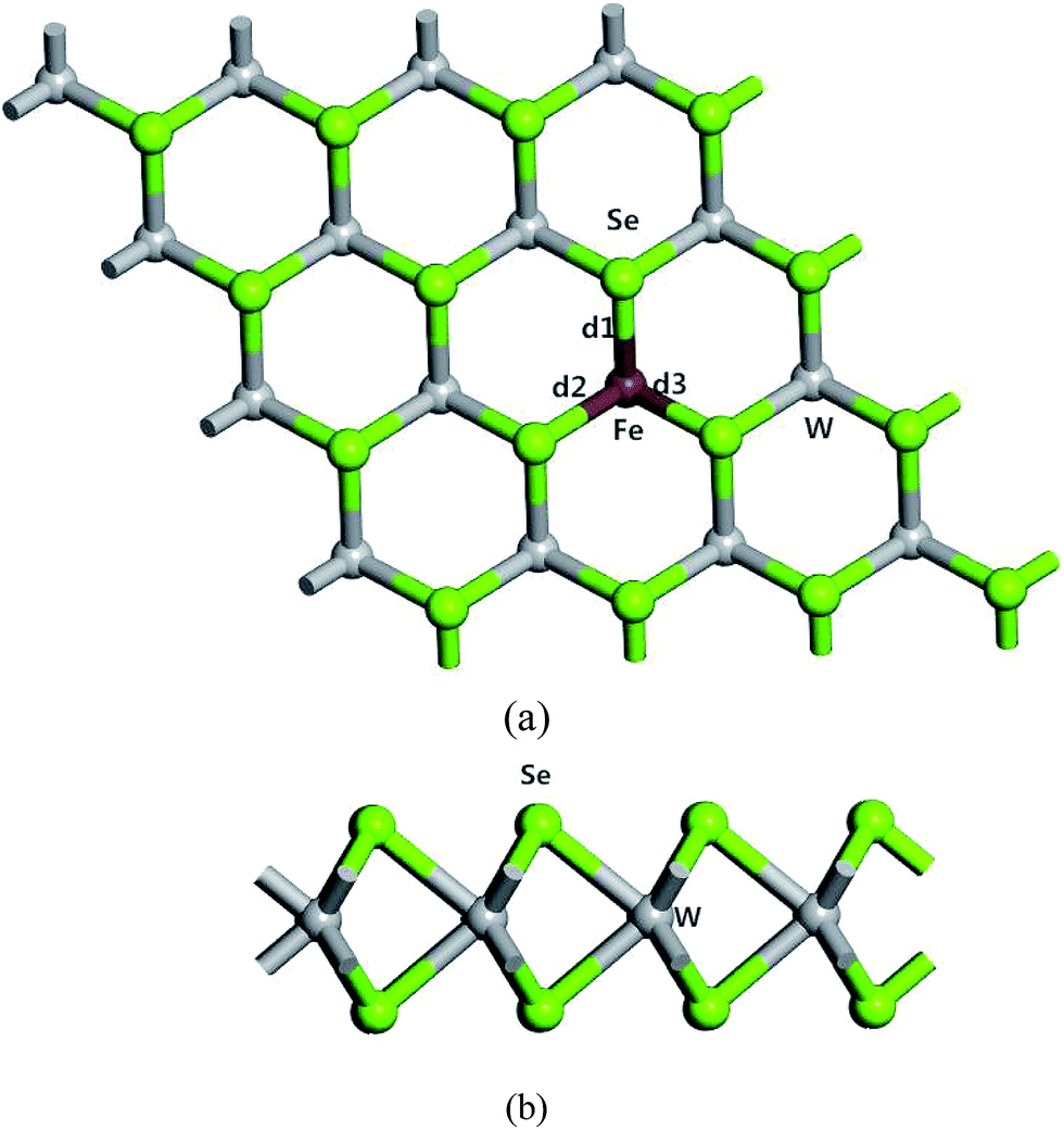 | ||
| Fig. 1 The schematic of Fe-doped WSe2 (a) top view and (b) side view. The green and grey balls represent Se and W atoms, respectively. d1, d2 and d3 represent the distance between the Fe and it's three nearest Se, respectively. | ||
Our calculations were performed within first-principles density functional theory (DFT) using the projector augmented wave (PAW) method35 was used within the Vienna ab initio simulation package (VASP).36 Electron exchange and correlation effects were described within the generalized gradient approximation (GGA) in the Perdew–Burke–Ernzerhof (PBE) parametrization.37 In all calculations, an energy cutoff of 500 eV for the plane-wave expansion of the wavefunctions was used. In order to check the convergence of the results with supercell size, the supercell of size 4 × 4 × 1 of the WSe2 primitive cell was used with a separation of 15 Å between two layers. The atomic positions were relaxed using a 9 × 9 × 1 K-points, all the structures are fully relaxed to minimize the total energy of the systems until a precision of 10−5 is reached. Both the atomic positions and cell parameters are optimized until the residual forces fall below 0.01 eV Å−1.
3. Results and discussion
In our work, we perform GGA calculations to investigate the influence of strain effect on the electronic and magnetic properties of Fe-doped WSe2. The average bond length dSe–Fe (defined as dSe–Fe = (d1 + d2 + d3)/3, where d1, d2 and d3 represent the bond lengths between the Fe atom and the three nearest neighbor (NN) Se atoms, respectively, as shown in Fig. 1) are shown in Fig. 2. The dW–Fe was calculated in the same way. It is obvious that the dW–Fe changes more quickly than dSe–Fe with increasing strain.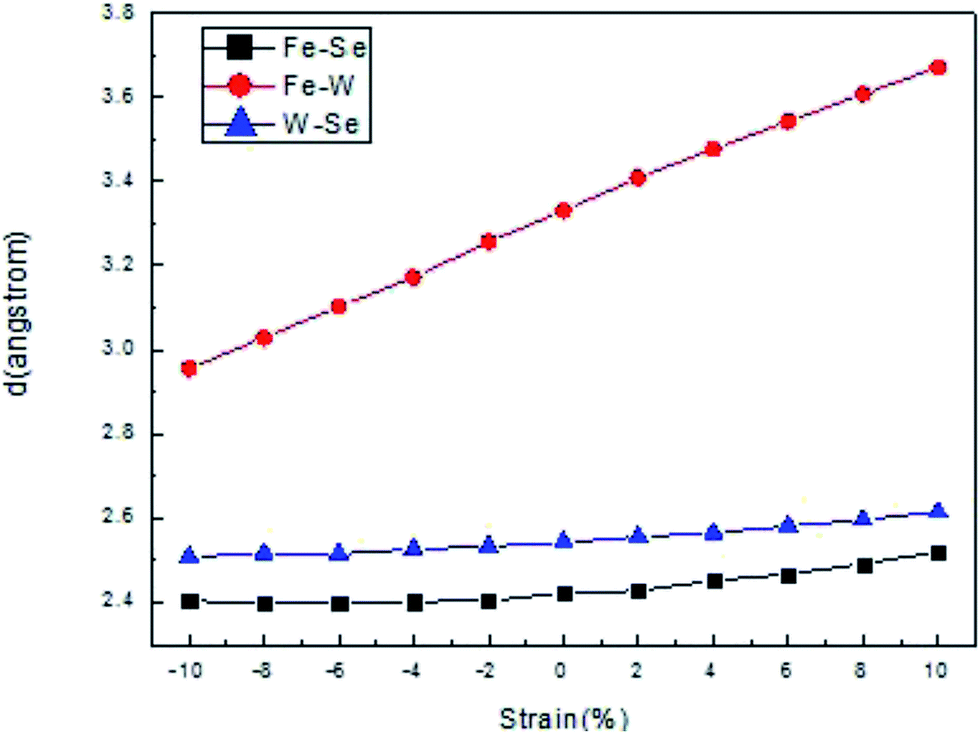 | ||
| Fig. 2 The average distance between Fe and its three nearest Se, Fe–Se (black line). The average distance between Fe and its nearest W, Fe–W (red line). The average distance between W and the nearest Se, W–Se (blue line). | ||
In the following, we present our calculation results on the effect of equibiaxial strain on the magnetic properties of Fe-doped WSe2. At the zero strain, we observed spin polarization in Fe-doped WSe2 and the magnetic moment is 1.902 μB. With the tensile strain increase to 10%, the magnetic moment enhanced to 2.117 μB slightly. Combining with bond length between the atoms, we can found that the increasing strain induces the change of the structure symmetry and the redistribution of intra-atomic d states, which changes the magnetic moments. When we applied compressive strain on Fe-doped WSe2, the magnetic moment are 1.863 μB (−2% strain) and 1.814 μB (−4% strain), respectively. Then its magnetism vanishes at −5% strain. It suggests that the excessive compressive strain changes WSe2 monolayer intrinsic properties and is meaningless. Through this analysis, we find that the strain plays an important role in electronic and magnetic properties for Fe-doped WSe2 monolayer. The results indicate that the Fe-doped WSe2 2D nanostructures can endure the strain from −4% to 10%. It is similar to ref. 38–40.
The band structures with and without strain are shown in Fig. 3. As we can see from the band structures without strain, the spin-up and spin-down band structures are not symmetric and show that the Fe-doped WSe2 is a magnetic semiconductor. The impurity states within the band gap are mainly from the Fe atom, whereas the contribution from the WSe2 can be neglected. While at 4% tensile strain, the band crossing at the Fermi level occurs with little dispersion in spin-up band structure, in spin-down band structure, there is a 0.183 eV half-metallic band gap. The half-metallic (HM) gap is an important parameter to determine application in spintronic devices, which is defined as a minimum of Ec and Ev, where Ec is the bottom energy of the minority-spin conduction band with respect to the Fermi level and Ev is the absolute value of the top energy of the minority-spin valence band, also with respect to the Fermi level. The calculated band structures show Fe-doped WSe2 has a half-metallic feature at 4% tensile strain. With the increase of tensile strain, it keeps half-metallic feature from 4% to 9% (see Table 1). According to this rule, the half-metallic gap is about 0.183, 0.166, 0.161, 0.176 eV, respectively, for strain = 4%, 6%, 8%, 9%. Then at 10% strain, both spin-up and spin-down band structure crossing at the Fermi level occur with little dispersion. It means that the Fe-doped WSe2 turn into metal at 10% tensile strain. When we apply the compressive strain on Fe-doped WSe2, we can see that it has half-metallic feature at −2% strain and then turns into magnetic metal at −4%. The system turns into the non-magnetic metal material from −5% to −10%. The system shows metal feature under larger compressive strain. Compared with tensile strain, the compressive strain is more effective on the electronic and magnetic properties of Fe-doped WSe2.
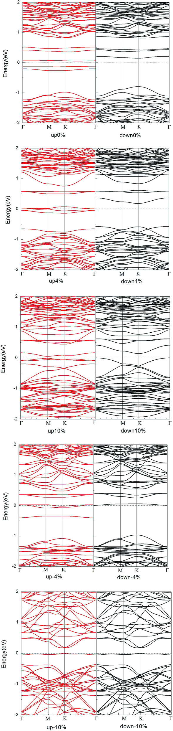 | ||
| Fig. 3 Spin-polarized band structures of Fe-doped WSe2 monolayer structures with strain 0%, 4%, 10%, −4%, and −10%, respectively. The red and black lines represent the spin-up and spin-down components, respectively. Where the Fermi level is indicated by the black imaginary line. | ||
| Strain (%) | −10 | −8 | −6 | −5 | −4 | −2 | 0 | 2 | 4 | 6 | 8 | 9 | 10 | |
|---|---|---|---|---|---|---|---|---|---|---|---|---|---|---|
| ΔEHM-gap (eV) | — | — | — | — | — | 0.149 | — | — | 0.183 | 0.166 | 0.161 | 0.176 | — | |
| Eform (eV) | W-rich | 20.825 | 13.966 | 8.957 | 7.653 | 5.527 | 3.444 | 2.349 | 2.563 | 3.584 | 5.453 | 8.693 | 10.267 | 11.422 |
| Se-rich | 19.129 | 12.269 | 7.261 | 5.957 | 3.831 | 1.748 | 0.653 | 0.867 | 1.888 | 3.759 | 6.397 | 8.571 | 9.726 | |
| Magnetic moment (μB) | 0 | 0 | 0 | 0 | 1.814 | 1.863 | 1.902 | 1.941 | 2.001 | 2.035 | 2.072 | 2.089 | 2.117 | |
In order to further understand the electronic characteristics in the Fe-doped WSe2 monolayer, the total density of states (TDOS) and the partial density of states (PDOS) for Fe-doped WSe2 monolayer with different stain are shown in Fig. 4 and 5, respectively. It is obvious that the polarized charges mainly arise from the localized 3d electrons of Fe atom, a little from the localized 5d electrons of the W atom and hardly from the localized 4p electrons of the Se atom near the Fermi level in Fig. 4. Fig. 5 further confirms that the Fe-doped WSe2 is magnetic semiconductor at 0% strain and turn into half-metal at 4% tensile strain. It keeps half-metal feature until applied 10% tensile strain and shows metal properties at 10% tensile strain. Under compressive strain, it has half-metallic feature at −2% and then becomes metal at −4%. From −5% to −10% strain, the spin-up and spin-down of DOS are symmetric and the magnetism disappears. The system turns into the non-magnetic metal material. These results indicate that the strain can change the electronic occupied of Fe-doped WSe2, which are analyzed to explain the strong strain effect on the electronic and magnetic properties.
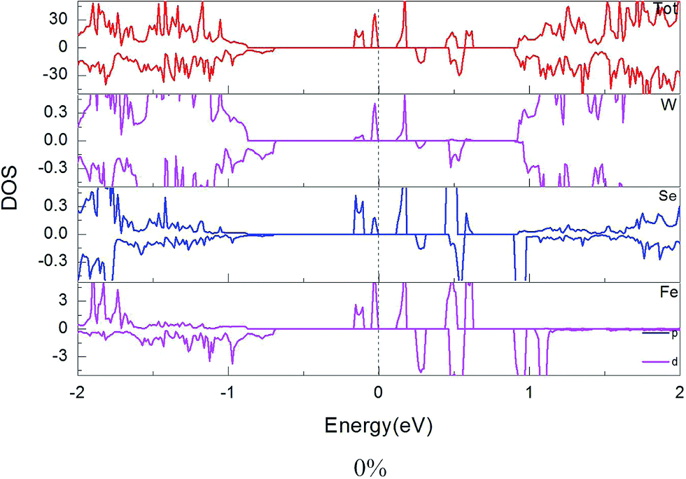 | ||
| Fig. 4 Total density of stats (TDOS) and partial density of states (PDOS) of Fe-doped WSe2 monolayer with 0% strain. | ||
 | ||
| Fig. 5 Total density of stats (TDOS) of Fe-doped WSe2 monolayer with different strain. | ||
The spin density of the Fe-doped monolayer WSe2 with different strain is shown in Fig. 6 can help us understand more deeply. It is noted that without strain, the neighboring Se atoms are antiferromagnetically coupled to the Fe atom and four nearest neighboring W atoms bonded to the Fe atom display ferromagnetic. At the 2% tensile strain, the neighboring Se atoms are antiferromagnetically coupled to the Fe atom, the p character of the spin-polarized orbitals of the Se atoms is clearly visible. Two atoms of six neighboring W atoms couple antiferromagnetically to the Fe atom, the rest bonded to the Fe atom display ferromagnetic. The d character of the spin-polarized orbitals of the W atoms is clearly visible. With the increasing of tensile strain, the antiferromagnetically of the two W atoms transform into ferromagnetic. The hybridization between the Fe 3d and the Se 4p or W 5d states enhance slowly and reach largest at 10% tensile strain. At the −2% compressive strain, the neighboring Se atoms are antiferromagnetically coupled to the Fe atom and the nearest neighboring W atoms bonded to the Fe atom display ferromagnetic. When the compressive strain reach −4%, both the neighboring Se atoms and the nearest neighboring W atoms bonded to the Fe atom display ferromagnetic mostly.
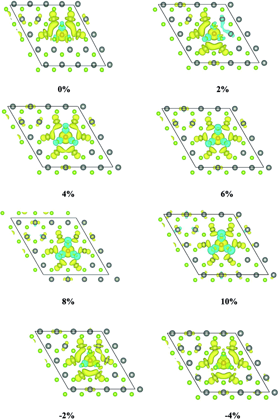 | ||
| Fig. 6 Spin density for a single Fe dopant atom in WSe2 monolayer when the strain is 0%, 2%, 4%, 6%, 8%, 10%, −2% and −4%. Yellow and cyan isosurfaces represent positive and negative spin densities (±0.001 e Å−3). | ||
To probe the stability of the Fe-doped WSe2 monolayer, the formation energy Eform can be calculated according to the following formula.41–45
| Eform = E(doped) − E(pure) + n(μW − μFe) |
4. Conclusion
In our work, we investigated the electronic and magnetic properties of Fe-doped WSe2 monolayer using the first-principles methods based on density functional theory. The compressive strain is more effective on electronic and magnetic properties in Fe-doped WSe2 monolayer than the tensile strain. Within the scope of the strain we applied, the largest magnetic moment is 2.117 μB at the 10% tensile strain and the minimum magnetic moment is 1.814 μB at the −4% compressive strain. The system undergoes a change from semiconductor to half-metal then to metal under strain. Further analysis show that strain changes the redistribution of charges and enhances the coupling between the 3d orbital of Fe atom, 5d orbital of W atom and 4p orbital of Se atom. Moreover, the formation energy calculations also indicate that it is energy favorable and relatively easier to incorporate Fe atom into the WSe2 monolayer under Se-rich experimental conditions. These results suggest that Fe-doped WSe2 monolayer might have important potential application in spintronic devices.Acknowledgements
This work is supported by a Grant from the National Natural Science Foundation of China (NSFC) under the Grant No. 11504092 and U1304518, National Undergraduate Training Programs for Innovation and Entrepreneurship (No. 201510476043), Science and technology research key project of education department of Henan province (No. 14A140012), and High Performance Computing Center of Henan Normal University.References
- A. K. Geim and K. S. Novoselov, Nat. Mater., 2007, 6, 183 CrossRef CAS PubMed.
- K. S. Novoselov, A. K. Geim, S. Morozov, D. Jiang, Y. Zhang, S. Dubonos, I. Grigorieva and A. Firsov, Science, 2004, 306, 666 CrossRef CAS PubMed.
- J. A. Wilson and A. D. Yoffe, Adv. Phys., 1969, 18, 193 CrossRef CAS.
- S. Sharma, C. A. Draxl, M. A. Khan, P. Blaha and S. Auluck, Phys. Rev. B: Condens. Matter Mater. Phys., 1999, 60, 12 CrossRef.
- E. Gourmelon, O. Lignier, H. Hadouda, G. Couturier, J. C. Bernède, J. Tedd, J. Pouzet and J. Salardenne, Sol. Energy Mater. Sol. Cells, 1997, 46, 115 CrossRef CAS.
- P. P. Hankare, A. H. Manikshete, D. J. Sathe, P. A. Chate, A. A. Patil and K. M. Garadkar, J. Alloys Compd., 2009, 479, 657 CrossRef CAS.
- K. S. Novoselov, D. Jiang, F. Schedin, T. J. Booth, V. V. Khotkevich, S. V. Morozov and A. K. Geim, Proc. Natl. Acad. Sci. U. S. A., 2005, 102(30), 10451–10453 CrossRef CAS PubMed.
- B. Radisavljevic, A. Radenovic, J. Brivio, V. Giacometti and A. Kis, Nat. Nanotechnol., 2011, 6(3), 147–150 CrossRef CAS PubMed.
- H. Fang, S. Chuang, T. C. Chang, K. Takei, T. Takahashi and A. Javey, Nano Lett., 2012, 12(7), 3788–3792 CrossRef CAS PubMed.
- Q. H. Wang, K. Kalantar-Zadeh, A. Kis, J. N. Coleman and M. S. Strano, Nat. Nanotechnol., 2012, 7(11), 699–712 CrossRef CAS PubMed.
- S. Z. Butler, S. M. Hollen, L. Cao, Y. Cui, J. A. Gupta, H. R. Gutiérrez, T. F. Heinz, S. S. Hong, J. Huang, A. F. Ismach, E. Johnston-Halperin, M. Kuno, V. V. Plashnitsa, R. D. Robinson, R. S. Ruoff, S. Salahuddin, J. Shan, L. Shi, M. G. Spencer, M. Terrones, W. Windl and J. E. Goldberger, ACS Nano, 2013, 7(4), 2898–2926 CrossRef CAS PubMed.
- M. Chhowalla, H. S. Shin, G. Eda, L. J. Li, K. P. Loh and H. Zhang, Nat. Chem., 2013, 5(4), 263–275 CrossRef PubMed.
- M. Xu, T. Liang, M. Shi and H. Chen, Chem. Rev., 2013, 113(5), 3766–3798 CrossRef CAS PubMed.
- D. Jariwala, V. K. Sangwan, L. J. Lauhon, T. J. Marks and M. C. Hersam, ACS Nano, 2014, 8(2), 1102–1120 CrossRef CAS PubMed.
- X. J. Zhang, X. C. Wang and W. B. Mi, Solid State Commun., 2015, 212, 35–40 CrossRef CAS.
- X. J. Zhang, W. B. Mi, X. C. Wang, Y. C. Cheng and U. Schwingenschlogl, Sci. Rep., 2014, 4, 7368 CrossRef CAS PubMed.
- M. Y. Yin, X. C. Wang, W. B. Mi and B. H. Yang, Comput. Mater. Sci., 2015, 99, 326–335 CrossRef CAS.
- N. Feng, W. B. Mi, Y. C. Cheng, Z. B. Guo, U. Schwingenschlögl and H. Bai, ACS Appl. Mater. Interfaces, 2014, 6, 4587–4594 CAS.
- N. Feng, W. B. Mi, Y. C. Cheng, Z. B. Guo, U. Schwingenschlogl and H. Bai, Sci. Rep., 2014, 4, 3987 Search PubMed.
- Z. Y. Zhu, Y. C. Cheng and U. Schwingenschlögl, Phys. Rev. B: Condens. Matter Mater. Phys., 2011, 84(15), 153402 CrossRef.
- D. Xiao, G. B. Liu, W. Feng, C. Xu and W. Yao, Phys. Rev. Lett., 2012, 108(19), 196802 CrossRef PubMed.
- H. Yuan, M. S. Bahramy, K. Morimoto, S. Wu, K. Nomura, B. J. Yang, H. Shimotani, R. Suzuki, M. Toh, C. Kloc, X. Xu, R. Arita, N. Nagaosa and Y. Iwasa, Nat. Phys., 2013, 9(9), 563–569 CrossRef CAS.
- G. Prasad and O. N. Srivastava, J. Phys. Appl. Phys., 1988, 21, 1028 CrossRef CAS.
- K. T. Chan, H. Lee and M. L. Cohen, Phys. Rev. B: Condens. Matter Mater. Phys., 2011, 83, 035405 CrossRef.
- H. Johll, H. C. Kang and E. S. Tok, Phys. Rev. B: Condens. Matter Mater. Phys., 2009, 79, 245416 CrossRef.
- H. Sevincli, M. Topsakal, E. Durgun and S. Ciraci, Phys. Rev. B: Condens. Matter Mater. Phys., 2008, 77, 195434 CrossRef.
- J. Li, M. L. Hu, Z. Yu, J. X. Zhong and L. Z. Sun, Chem. Phys. Lett., 2012, 532(14), 40–46 CrossRef CAS.
- T. O. Wehling, A. I. Lichtenstein and M. I. Katsnelson, Phys. Rev. B: Condens. Matter Mater. Phys., 2011, 84, 235110 CrossRef.
- J. J. He, S. Y. Ma, P. Zhou, C. X. Zhang, C. Y. He and L. Z. Sun, J. Phys. Chem. C, 2012, 116(50), 26313–26321 CAS.
- Y. Qu, S. L. Chang, S. Q. Qin and J. B. Li, Phys. Lett. A, 2013, 377(19), 1362–1367 Search PubMed.
- Y. C. Cheng, Z. Y. Zhu, W. B. Mi, Z. B. Guo and U. Schwingenschlögl, Phys. Rev. B: Condens. Matter Mater. Phys., 2013, 8(7), 10040 Search PubMed.
- H. Shu, P. Luo, P. Liang, D. Cao and X. Chen, ACS Appl. Mater. Interfaces, 2015, 7(14), 7534–7541 CAS.
- Y. G. Zhou, X. T. Zu, F. Gao, H. F. Lv and H. Y. Xiao, Appl. Phys. Lett., 2009, 95(12), 123119 CrossRef.
- Y. G. Zhou, P. Yang, Z. G. Wang, X. T. Zu, H. Y. Xiao, X. Sun and F. Gao, Phys. Chem., 2011, 13(16), 7378–7383 CAS.
- P. E. Blochl, Phys. Rev. B: Condens. Matter Mater. Phys., 1994, 50, 17953 CrossRef.
- G. Kresse and J. Furthmuller, Phys. Rev. B: Condens. Matter Mater. Phys., 1996, 54, 11169 CrossRef CAS.
- J. P. Perdew, K. Burke and M. Ernzerhof, Phys. Rev. Lett., 1996, 77, 3865 CrossRef CAS PubMed.
- S. Bertolazzi, J. Brivio and A. Kis, ACS Nano, 2011, 5, 9703–9709 CrossRef CAS PubMed.
- R. C. Cooper, C. Lee, C. A. Marianetti, X. Wei, J. Hone and J. W. Kysar, Phys. Rev. B: Condens. Matter Mater. Phys., 2013, 87, 035423 CrossRef.
- T. Li, Phys. Rev. B: Condens. Matter Mater. Phys., 2012, 85, 235407 CrossRef.
- C. X. Xia, Y. T. Peng, S. Y. Wei and Y. Jia, Acta Mater., 2013, 61, 7720–7725 CrossRef CAS.
- C. X. Xia, Y. T. Peng, H. Zhang, T. X. Wang, S. Y. Wei and Y. Jia, Phys. Chem. Chem. Phys., 2014, 16, 19674 RSC.
- Y. T. Peng, C. X. Xia, H. Zhang, T. X. Wang, S. Y. Wei and Y. Jia, Phys. Chem. Chem. Phys., 2014, 16, 18799 RSC.
- X. Zhao, T. X. Wang, G. T. Wang, X. Q. Dai, C. X. Xia and L. Yang, Appl. Surf. Sci., 2016, 383, 151–158 CrossRef CAS.
- X. Zhao, C. X. Xia, T. X. Wang and X. Q. Dai, J. Alloys Compd., 2016, 654, 574–579 CrossRef CAS.
- R. Mishra, Z. Wu, S. J. Pennycook, S. T. Pantelides and J. C. Idrobo, Phys. Rev. B: Condens. Matter Mater. Phys., 2013, 88, 144409 CrossRef.
| This journal is © The Royal Society of Chemistry 2016 |