
Positive/negative electrocaloric effect induced by defect dipoles in PZT ferroelectric bilayer thin films†
Tiandong Zhanga,
Weili Li*ab,
Yafei Houa,
Yang Yua,
Wenping Caoa,
Yu Fenga and
Weidong Fei*ac
aSchool of Materials Science and Engineering, Harbin Institute of Technology, Harbin 150001, People’ Republic of China. E-mail: wlli@hit.edu.cn; wdfei@hit.edu.cn
bNational Key Laboratory of Science and Technology on Precision Heat Processing of Metals, Harbin Institute of Technology, Harbin 150001, People’ Republic of China
cState Key Laboratory of Advanced Welding and Joining, Harbin Institute of Technology, Harbin 150001, People’ Republic of China
First published on 22nd July 2016
Abstract
Double hysteresis loops induced by defect dipoles are obtained in PbZr0.52Ti0.48O3/PbZr0.8Ti0.2O3 ferroelectric bilayer thin films prepared by a sol–gel method. The migration of the defect dipoles related to the temperature and applied electric field is investigated in detail, which has a deep influence on the polarization due to the effect of the domain pinning caused by defect dipoles. Meanwhile, the electrocaloric effect based on double hysteresis loops induced by defect dipoles has been studied. The coexistence of a negative electrocaloric effect and positive electrocaloric effect has been achieved in PbZr0.52Ti0.48O3/PbZr0.8Ti0.2O3 bilayer films, ΔT = −8.4 K at 155 °C, and ΔT = 4.4 K at 45 °C. The amplifying effect of the applied electric field in the PZr0.8Ti0.2O3 layer films plays an important role in the excellent negative electrocaloric values. More interestingly, the coexistence of the negative electrocaloric and positive electrocaloric effect can be obtained by regulating the applied electric field, which is beneficial to enhancing the cooling efficiency during the cycling of the applied electric field.
1. Introduction
Caloric effects have attracted a lot of attention recently in the field of the energy conversion.1 The electrocaloric effect (abbreviated as ECE) is an analogue of the magnetocaloric effect,2,3 which appears as a very promising alternative to vapour compression refrigeration and IC thermal management.4 The ECE of PbZr0.95Ti0.05O3 thin films and PVDF copolymer films with a giant ECE at adiabatic temperature ΔT −12 K were seeds of an explosive growth in electrocaloric research.5,6 So far various ECE materials, including bulk ceramic materials and thin films materials, have been systematically studied, and higher ΔT values in the thin films were obtained due to the much higher applied electric field compared with that of their bulk materials, for example, the BaTiO3 thick films exhibited a giant ECE of ΔT = 7.1 K and ΔS = 10.1 J K−1 kg−1 at 800 kV cm−1,7 wherein the ΔT was just 0.9 K with a lower electric field of 12 kV cm−1 in the single crystal BaTiO3.8As the research moves along, except the conventional positive ECE (abbreviated as PECE), interestingly and unexpectedly, the negative ECE (abbreviated as NECE) was found in relaxor ferroelectrics and antiferroelectrics. It was reported that the NECE may enlarge the electrocaloric family and enhance the efficiency of ferroelectric cooling device in combination with the PECE.4 A NECE in PMN-PT ceramics was observed by Peräntie and Axelsson,9,10 which was caused by the electric field induced rhombohedral and orthorhombic phase transition. And the NECE in NBT-BT ceramics was attributed to the phase transition of tetragonal antiferroelectric (AFE) phase and tetragonal ferroelectric (FE) phase.11,12 According to the Geng' results, the NECE in PLZT based materials was originated from the field induced noncollinearity of the polarization, and the application of a modest electric field in AFEs or FEs will generally increase the entropy by misaligning the dipoles, therefore generating the NECE,13,14 which was accordance with the prediction proposed by I. Ponomareva and S. Lisenkov.15 Through the thermodynamics analysis and phase field simulations method, H. H. Wu et al. reported a technology to universalize the NECE by applying mechanical compression in perovskite ferroelectrics.16,17 Furthermore, PbZr0.53Ti0.47O3/CoFe2O4 multi-layered nanostructures were found to display a NECE caused by magnetro-electric coupling effect.18 Chi et al. reported that the multilayer thin films exhibit excellent pyroelectric effect which is corresponding to the converse effect of electrocaloric effect.19,20
Based on the aforementioned viewpoints, there is no doubt that the NECE refers to the entropy increased by applying electric field. Although the NECE was originated from different mechanisms, the double hysteresis loops (PE loops) may be an important pre-conditions. The double PE loops were usually observed in AFE and FE ceramics, which were caused by the antiparallel dipoles and defect dipoles, respectively.21–24 Beyond that, it was exceptional phenomenon that the double PE loops were discovered in PbZr0.8Ti0.2O3 and HoMnO3 ferroelectric thin films,25,26 which was associated with the realignment of defect dipoles. In addition, the competition among the intrinsic ferroelectric coupling at the interface between PbTiO3/PbZr0.3Ti0.7O3 bilayer thin films also gave rise to the double PE loops.27,28 However, the ECE in FE films resulting from double PE loops induced by defect dipoles was few studied, especially for the bilayer or multilayer thin films.
Recently, the authors have observed a giant ECE (24.8 K around 125 °C) in PZT bilayer thin films, which is induced by the amplifying effect of the applied electric field.29 In order to take the full advantage of the amplifying effect of the applied electric field, the bilayer thin films' structure is also employed in this work. The electric field amplification can be realized in bilayer thin films by the uneven dielectric constant of individual layer, so the MPB composition PbZr0.52Ti0.48O3 (abbreviated as PZ0.52T0.48) with a higher εr (2038 at 1 kHz) is selected as the top layer film, and we choose the Zr-rich PbZr0.8Ti0.2O3 (abbreviated as PZ0.8T0.2) with a lower εr (1068 at 1 kHz) as the bottom layer films (see in Fig. S1, ESI†), wherein the double PE loops induced by defect dipoles have been obtained.25 The double PE loops and expected NECE are found in PbZr0.52Ti0.48O3/PbZr0.8Ti0.2O3 (abbreviated as PZ0.52T0.48/PZ0.8T0.2) ferroelectric bilayer thin films in this work. The mechanisms of this remarkable double PE loops and NECE are discussed in detail. More interestingly, it is found that the coexistence of the PECE and NECE can be obtained by regulating the amplitude of the applied electric field.
2. Results and discussion
X-ray diffraction measurement shows a pure perovskite phase as shown in Fig. 1(a). It is found inset in Fig. 1(a) that the rhombohedral phase and tetragonal phase are co-existed in PZ0.52T0.48/PZ0.8T0.2 thin films. According to the SEM and AFM scanning results as shown in Fig. 1(b) and (c), the thickness and grain size of PZ0.52T0.48/PZ0.8T0.2 films are about 350 nm and 135 nm, respectively. | ||
| Fig. 1 (a) XRD patterns, (b) cross-section image of SEM scanning, (c) surface image of AFM scanning of PZ0.52T0.48/PZ0.8T0.2 bilayer films. | ||
Fig. 2(a)–(d) show the room temperature polarization behavior of the bilayer films with different applied electric fields. It is exciting that the double PE loops are observed in PZ0.52T0.48/PZ0.8T0.2 ferroelectric bilayer films. To further confirm the AFE-like behavior of the bilayer films, the voltage dependence of capacitance curves (CV curves) measured at different frequencies are given in Fig. 3. The butterfly curves with a valley are observed when the applied voltage is lower than 10 V, which indicates that the AFE-like behavior exists in PZ0.52T0.48/PZ0.8T0.2 bilayer films. The possible origin for the double PE loops in PZ0.52T0.48/PZ0.8T0.2 bilayer films has not been yet elucidated but inferred to be induced by the domain pinning by defect dipoles,25,26 so it is necessary for us to investigate whether the double PE loops in PZ0.52T0.48/PZ0.8T0.2 bilayer films are caused by defect dipoles.
 | ||
| Fig. 2 PE loops of PZ0.52T0.48/PZ0.8T0.2 bilayer films with different applied electric fields, (a) 143 kV cm−1, (b) 282 kV cm−1, (c) 426 kV cm−1, (d) 566 kV cm−1. | ||
 | ||
| Fig. 3 CV curves of PZ0.52T0.48/PZ0.8T0.2 bilayer films with different applied voltage, (a) 5 V, (b) 8 V, (c) 10 V, (d) 12 V. | ||
If the double PE loops in PZ0.52T0.48/PZ0.8T0.2 ferroelectric bilayer films are caused by the restoring forces provided by the “immobile” defect dipoles, it is well believed that the stability of defect dipoles is sensitive to the temperature.22 So the temperature dependence of polarization is an efficient way to confirm the presence of defect dipoles and to observe the migration of defect dipoles in the macroscopic perspective. As shown in Fig. 4(a) and (b), it can be seen that the constricted PE loops measured at 100 Hz becomes “opened” near a critical temperature, which should be attributed to the high migration rate of the defect dipoles at high temperature. The critical temperature is about 200 °C when the electric field is 143 kV cm−1, and it decreases to 150 °C when the higher electric field (566 kV cm−1) is applied. It implies that higher applied electric field is also beneficial to the migration of defect dipoles. In addition, it can be found that as the measured frequency decreases, the PE loops open gradually and the remnant polarization value increases rapidly at low frequencies as shown inset in Fig. 4(a). It indicates that if the polarization switching time is long enough, the defect dipoles will migrate and rotate along the polarization direction.
 | ||
| Fig. 4 PE loops with different applied electric fields at selected temperatures (a) under 143 kV cm−1 (measured frequency dependence of the remnant polarization values is given in inset), (b) under 566 kV cm−1. | ||
It has been reported that the double PE loops are also obtained in PZ0.8T0.2 single layer films,25 this result supports that the effect of the domain pinning induced by defect dipoles gives rise to the double PE loops in PZ0.8T0.2 single layer films. The XPS results have been provided to support the existence of the oxygen vacancy (see in Fig. S1, ESI†). And in order to confirm the existence of defect dipoles in PZ0.8T0.2 single layer films, the PE loops and CV curves for the single layer thin films are also investigated. The double PE loops and the butterfly CV curves are observed in PZ0.8T0.2 single layer films (as shown in Fig. S2, ESI†). The schematic diagram of a possible mechanism for the origin of double PE loops induced by defect dipoles in PZ0.52T0.48/PZ0.8T0.2 bilayer films is given in Fig. 5. The oxygen vacancies ( ) associated with defect dipoles are simultaneously created by charge compensation, which are introduced unintentionally during the PZ0.8T0.2 films growth process. Based on the symmetry conforming principle, the defect dipoles tend to adopt a statistical symmetry that follows the crystal symmetry.21,30 The defect dipoles makes a defect polarization (PD) aligning along the spontaneous polarization (PS), wherein the spontaneous polarization PS along 〈111〉R direction in the rhombohedral ferroelectrics as shown in Fig. 5(a). When an electric field (E) is applied, PS orientation changes to align along E direction, but the defect dipoles symmetry and the associated PD can not have a sudden change with E, wherein still in the original direction. The PD provides an intrinsic restoring force acting on PS as shown in Fig. 5(b1), leading to a macroscopic double PE loops at room temperature (RT). With the temperature increasing, the constricted PE loops become opened gradually due to the high migration rate of the defect dipoles at higher temperature (shown in Fig. 5(b2) and (b3)). The constricted PE loops, under the application of lower E and higher E, become fully opened around T2 and T1 (T1 < T2), respectively. It suggests that the migration of defect dipoles is also related to the amplitude of the applied E. And the higher E and the larger polarization induced by higher E also provide an attractive electric field force, which is beneficial to the migration of the defect dipoles. In this work, T2 is about 200 °C under a lower electric field (143 kV cm−1), and T1 is around 150 °C with a higher electric field (566 kV cm−1), as shown in Fig. 4(a) and (b).
 | ||
| Fig. 5 Mechanism of double hysteresis loops induced by defect dipoles in PZ0.52T0.48/PZ0.8T0.2 bilayer films, and the schematic of the relationship between the migration of the defect dipoles and temperature, applied electric field. (a) Defect symmetry follows crystal symmetry, (b) and (c) shows the unstable state of defect dipoles at different temperature T and applied electric field E. (b1) RT, lower E, (b2) T1, lower E, (b3) T2, lower E, (c1) RT, higher E, (c2) T1, higher E, (c3) T2, higher E, wherein RT < T1 < T2. | ||
Before the investigation of the effect of the double PE loops induced by defect dipoles on ECE in PZ0.52T0.48/PZ0.8T0.2 bilayer thin films, it is necessary to investigate the phase transition behavior. As shown in Fig. 6(a), there is no significant structural phase transition according the results of the dielectric spectrum with temperature and the evolution of (200)pc diffraction peaks with temperature. However, the lower dielectric loss value obtained around 160 °C may indicate that the effect of domain pinning induced by defect dipoles is weakened, which lead to the decreasing dielectric loss values, and the broad dielectric loss peaks near room temperature may be caused by the domain rotation process in PZ0.52T0.48 layer as shown in Fig. 6(b). In order to further study the effect of temperature on the migration rate of defect dipoles, the temperature dependence of CV curves measured at 1 MHz are given in Fig. 6(c) and (d). The twin peaks of CV curves are observed at room temperature due to the domain pinning by defect dipoles, which are consistent with the characteristics of double hysteresis loops. It also implies that the polarization behavior is affected by defect dipoles. With the temperature increasing, the twin peaks disappear completely at about 200 °C due to the vanished domain pinning effect, which is induced by the high migration rate of defect dipoles at high temperature. Then, the twin peaks appear gradually with the temperature decreasing due to the reappearance of the domain pinning effect induced by the low migration rate of defect dipoles.
 | ||
Fig. 6 (a) Temperature dependence of dielectric constant, the inset shows the evolution of (200)pc diffraction peaks, (b) dielectric loss tan![[thin space (1/6-em)]](https://www.rsc.org/images/entities/char_2009.gif) δ, (c) CV curves dependence on the temperature increasing, (d) CV curves dependence on the temperature decreasing. δ, (c) CV curves dependence on the temperature increasing, (d) CV curves dependence on the temperature decreasing. | ||
Assuming the reversible adiabatic changes following the Maxwell relationship  , the temperature change ΔT and entropy change ΔS for a material of density ρ with specific heat capacity C are expressed as follows:5,31
 | (1) |
 | (2) |
Values of ∂P/∂T are obtained from fourth-order polynomial fit to the P(T) data extracted from the upper branches of PE loops in E > 0, see the inset of Fig. 7(a) and (b).
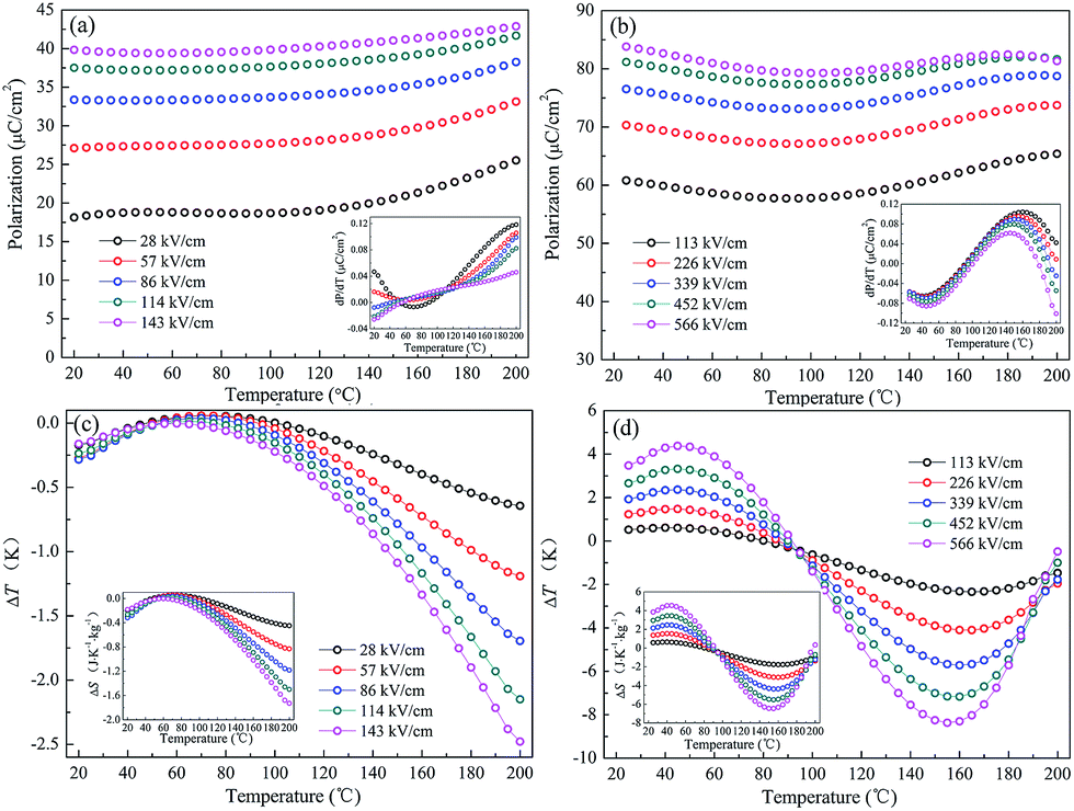 | ||
| Fig. 7 Polarization (P) dependence on temperature (T) at selected electric fields, the inset shows the ∂P/∂T values (a) measured under 143 kV cm−1, (b) measured under 566 kV cm−1, ΔT of bilayer thin films at selected electric field, the inset shows the ΔS values (c) measured under 143 kV cm−1, (d) measured under 566 kV cm−1. | ||
The PZ0.52T0.48/PZ0.8T0.2 films can be considered as the Zr-rich lead based thin films, and the heat capacity C = 330 J K−1 kg−1 and density ρ = 8.3 kg cm−3 can be selected for the Zr-rich lead-based thin films.5,32 In Fig. 7(c), ΔT = −2.5 K and ΔS = −1.7 J K−1 kg−1 are obtained at 200 °C under the application of an electric field ∼143 kV cm−1. When the applied electric field is 566 kV cm−1, the coexistence of NECE and PECE has been found, as shown in Fig. 7(d). The NECE with ΔT = −8.4 K, ΔS = −6.4 J K−1 kg−1 at 155 °C, and PECE with ECE ΔT = 4.4 K, ΔS = 4.5 J K−1 kg−1 at 45 °C are achieved. It is well believed that the driving force of ECE is the change of entropy associated with the electric field variation, in other words, which corresponds to the realignment of the defect dipoles under the application or withdrawal of applied electric fields. A possible mechanism for NECE is that the weakened effect of domain pinning by defect dipoles leads to the increase of polarization with the temperature increasing, which gives rise to the increase of ΔS when the electric field is applied. In addition, according to the Gauss law, the electric field amplification can be realized in bilayer thin films by the uneven dielectric constant of individual layer, the amplifying effect of the applied electric field in PZ0.8T0.2 layer films may also play an important role on the excellent NECE.29 It is also worth mentioning that the peaks of the optimal NECE values are shifted to the lower temperature with the applied electric field increasing, which are consistence with the fully opened temperature of the double PE loops. The PECE (ΔT = 4.4 K at 45 °C) is also observed when a higher electric field ∼566 kV cm−1 is applied, the phase boundaries in PZ0.52T0.48 layer may act as potential resources of high ΔS values due to more lattice entropy induced by a higher applied electric field. The coexistence of the NECE and PECE is beneficial for us to enhance the cooling efficiency during the cycling of an applied electric field.13,14,16
Although originated from different mechanisms, the NECE have been found in many kinds of materials. For comparison, Table 1 lists the NECE of representative materials. To fully utilize the PECE combined with NECE may be an effective way to enhance the cooling efficiency, for example, when the applied electric field is increased at NECE operating temperature, the NECE works, and then, at PECE operating temperature, the applied electric field is decreased from maximum to zero, the PECE works. It is worth expecting that a solid-state cooling device based on the coexistence of PECE and NECE would be achieved with the development of technology.
| Materials | ΔT (K) | ΔS (J K−1 kg−1) | ΔE (kV cm−1) | T (°C) | Reference |
|---|---|---|---|---|---|
| a P indicates the PECE while N stands for NECE; f refers to thin films, while bs and bc correspond to single crystal and bulk ceramics. | |||||
| PZ0.52T0.48/PZ0.8T0.2 bilayer filmsNf | −2.5 | −1.7 | 143 | 200 | This work |
| PZ0.52T0.48/PZ0.8T0.2 bilayer filmsPNf | −8.4 | −6.4 | 566 | 155 | |
| 4.4 | 4.5 | 566 | 45 | ||
| Na0.5Bi0.5TiONbc3 | −0.33 | −0.41 | 50 | 140 | 11 |
| Pb0.97La0.02Zr0.95Ti0.05ONf3 | −5 | — | 303 | 30 | 13 |
| Pb0.97La0.02Zr0.95Ti0.05OPf3 | 8 | — | 308 | 225 | |
| PbZr0.53Ti0.47O3/CoFeO4-L3Nf | −52.2 | −94.23 | 370 | −91 | 18 |
| Eu-doped PbZrONf3 | −6.62 | −5.42 | 709 | 130 | 33 |
| Na0.5Bi0.5TiO3–0.06BaTiONbc3 | −2.4 | — | 70 | 50 | 12 |
| Na0.5Bi0.5TiO3–0.04BaSrTiONbc3 | −2.1 | — | 60 | 80 | |
| Sr0.5Ba0.5Nb2ONbs6 | −1.4 | — | 15 | 127 | 34 |
| Pb0.97La0.02Zr0.66Sn0.23Ti0.11ONbs3 | −0.14 | −0.3 | 30 | 125 | 14 |
| Pb0.97La0.02Zr0.66Sn0.23Ti0.11OPbs3 | 0.75 | 1.5 | 30 | 160 | |
| PbMg1/3Nb2/3–0.3PbTiONbs3 | −0.15 | — | 10 | 80 | 35 |
| PbMg1/3Nb2/3–0.3PTiOPbs3 | 0.65 | — | 10 | 135 | |
3. Experimental
The PZ0.52T0.48/PZ0.8T0.2 bilayer thin films were fabricated on a Pt(111)/Ti/SiO2/Si substrate using sol–gel method. Pb(CH3COO)2·3H2O was dissolved in 2-methoxyethanol and refluxed at 120 °C for 30 min, and then zirconium n-propoxide and titanium isopropoxide were added into the above solution when it cooled down to room temperature. After refluxing for another 60 min, the concentration of the solution was adjusted to 0.4 mol L−1 by adding 2-methoxyethanol. After aging the precursor solution for 24 h, PZ0.52T0.48/PZ0.8T0.2 bilayer thin films were deposited on Pt(111)/Ti/SiO2/Si substrates through spin coating process, the individual PZ0.52T0.48 and PZ0.8T0.2 layer films have a equal thickness. Each layer was followed by pyrolysis at 375 °C for 3 min, and then the bilayer thin films were annealed in RTA at 700 °C for 5 min.The crystalline structures of the prepared thin films were analyzed by a Philips X′ pert X-ray diffractometer (XRD) with Cu Kα radiation generated at 40 kV and 40 mA. The cross-section micrograph of the thin films was performed by SEM (Helios Nanolab600i). For further electrical properties measurements, platinum electrodes with a size of 3.14 × 10⁻⁴ cm2, as the top electrode, were deposited by DC magnetron sputtering. The ferroelectric properties were characterized by a Radiant Precision Workstation Ferroelectric Measurement System, and the PE loops dependence on the temperature was measured at a frequency of 100 Hz at a 5 °C interval from 25 °C to 200 °C by Sigma heating system. With the help of Agilent 4294A precision impedance analyzer, temperature dependence of dielectric properties of the samples was measured at different frequency with a 500 mV ac amplitude. The capacitance with the applied voltage of the samples was measured at different frequencies with a 50 mV ac amplitude.
4. Conclusions
The double hysteresis loop caused by defect dipoles is discovered in PZ0.52T0.48/PZ0.8T0.2 bilayer thin films. The effects of the temperature and applied electric field on the migration ability of defect dipoles have been studied systematically. The coexistence of NECE and PECE has been found in PZ0.52T0.48/PZ0.8T0.2 bilayer films, the NECE ΔT = −8.4 K at 155 °C and PECE ΔT = 4.4 K at 45 °C. Meanwhile, a possible mechanism associated with defect dipoles for NECE is proposed. And the coexistence of the NECE and PECE is beneficial to enhance the cooling efficiency during the cycling of the applied electric field.Acknowledgements
The authors gratefully acknowledge support from Natural Science Foundation of China (Grant No. 11272102 and 51471057).References
- J. F. Scott, Annu. Rev. Mater. Res., 2011, 41, 229–240 CrossRef CAS.
- X. Moya, S. Kar-Narayan and N. D. Mathur, Nat. Mater., 2014, 13, 439–450 CrossRef CAS PubMed.
- X. Moya, E. Defay, V. Heine and N. D. Mathur, Nat. Phys., 2015, 11, 202–205 CrossRef CAS.
- T. Correia and Q. Zhang, Electrocaloric Materials: New Generation of Cooler, Springer Verlag, Berlin, Germany, 2014 Search PubMed.
- A. S. Mischenko, Q. Zhang, R. W. Whatmore, J. F. Scott and N. D. Mathur, Science, 2006, 311, 1270 CrossRef CAS PubMed.
- B. Neese, B. J. Chu, S. G. Lu, Y. Wang, E. Furman and Q. M. Zhang, Science, 2008, 321, 821 CrossRef CAS PubMed.
- Y. Bai, G. P. Zheng, K. Ding, L. J. Qiao, S. Q. Shi and D. Guo, J. Appl. Phys., 2011, 110, 094103 CrossRef.
- X. Moya, E. Stern-Taulats, S. Crossley, D. González-Alonso, S. Kar-Narayan, A. Planes, L. Mañosa and N. D. Mathur, Adv. Mater., 2013, 25, 1360–1365 CrossRef CAS PubMed.
- J. Peräntie, J. Hagberg, A. Uusimäki and H. Jantunen, Phys. Rev. B: Condens. Matter Mater. Phys., 2010, 82, 134119 CrossRef.
- A.-K. Axelsson, F. L. Goupil, L. J. Dunne, G. Manos, M. Valant and N. M. Alford, Appl. Phys. Lett., 2013, 102, 102902 CrossRef.
- Y. Bai, G. P. Zheng and S. Q. Shi, Mater. Res. Bull., 2011, 46, 1866–1869 CrossRef CAS.
- S. Uddin, G. P. Zheng, Y. Iqbal, R. Ubic and J. H. Yang, J. Appl. Phys., 2013, 114, 213519 CrossRef.
- W. P. Geng, Y. Liu, X. J. Meng, L. Bellaiche, J. F. Scott, B. Dkhil and A. Q. Jiang, Adv. Mater., 2015, 27, 3165–3169 CrossRef CAS PubMed.
- F. P. Zhuo, Q. Li, J. H. Gao, Y. J. Wang, Q. F. Yan, Y. L. Zhang, X. Q. Xi, X. C. Chu and W. W. Cao, Appl. Phys. Lett., 2016, 108, 082904 CrossRef.
- I. Ponomareva and S. Lisenkov, Phys. Rev. Lett., 2012, 108, 167604 CrossRef CAS PubMed.
- H. H. Wu, J. M. Zhu and T. Y. Zhang, Nano Energy, 2015, 16, 419–427 CrossRef CAS.
- H. H. Wu, J. Zhu and T. Y. Zhang, Phys. Chem. Chem. Phys., 2015, 17, 23897–23908 RSC.
- G. Vats, A. Kumar, N. Ortega, C. R. Bowen and R. S. Katiyar, Energy Environ. Sci., 2016, 9, 1335–1345 CAS.
- Q. G. Chi, X. Wang, W. L. Li, W. D. Fei and Q. Q. Lei, Appl. Phys. Lett., 2011, 98, 242903 CrossRef.
- Q. G. Chi, J. F. Dong, C. H. Zhang, X. Wang and Q. Q. Lei, J. Mater. Chem. C, 2016, 4, 4442 RSC.
- X. B. Ren, Nat. Mater., 2004, 3, 91–94 CrossRef CAS PubMed.
- D. M. Lin, K. W. Kwok, H. L. Wong and L.-W. Chan, J. Am. Ceram. Soc., 2009, 92, 1362–1365 CrossRef CAS.
- H. Tian, B. Yao, P. Tan, Z. X. Zhou, G. Shi, D. W. Gong and R. Zhang, Appl. Phys. Lett., 2015, 106, 102903 CrossRef.
- R. A. Maier, T. A. Pomorski, P. M. Lenahan and C. A. Randall, J. Appl. Phys., 2015, 118, 164102 CrossRef.
- Y. T. Pu, J. L. Zhu, X. H. Zhu, Y. S. Luo, M. S. Wang, X. H. Li, J. Liu, J. G. Zhu and D. Q. Xiao, J. Appl. Phys., 2011, 109, 044102 CrossRef.
- D. Lee, H. S. Kim, S. Y. Jang, K. W. Joh, T. W. Noh, J. Yu, C. E. Lee and J.-G. Yoon, Phys. Rev. B: Condens. Matter Mater. Phys., 2010, 81, 012101 CrossRef.
- L. L. Sun, O. K. Tan and W. G. Zhu, J. Appl. Phys., 2006, 99, 094108 CrossRef.
- J. G. Wu, J. L. Zhu, D. Q. Xiao and J. G. Zhu, Appl. Phys. Lett., 2007, 91, 212905 CrossRef.
- T. D. Zhang, W. L. Li, W. P. Cao, Y. F. Hou, Y. Yu and W. D. Fei, Appl. Phys. Lett., 2016, 108, 162902 CrossRef.
- Z. Y. Feng and X. B. Ren, Phys. Rev. B: Condens. Matter Mater. Phys., 2008, 77, 134115 CrossRef.
- Y. Zhao, X. H. Hao and Q. Zhang, ACS Appl. Mater. Interfaces, 2014, 6, 11633–11639 CAS.
- Y. Zhao, X. H. Hao and Q. Zhang, J. Mater. Chem. C, 2015, 3, 1694–1699 RSC.
- M. Ye, T. Li, Q. Sun, Z. K. Liu, B. L. Peng, C. W. Huang, P. Lin, S. M. Ke, X. R. Zeng, X. Peng, L. Chen and H. T. Huang, J. Mater. Chem. C, 2016, 4, 3375–3378 RSC.
- I. Bhaumik, S. Ganesamoorthy, R. Bhatt, A. K. Karnal, P. K. Gupta, S. Takekawa and K. Kitamura, Europhys. Lett., 2014, 107, 47001 CrossRef.
- F. L. Goupil, A. Berenov, A.-K. Axelsson, M. Valant and N. M. Alford, J. Appl. Phys., 2012, 111, 124109 CrossRef.
Footnote |
| † Electronic supplementary information (ESI) available: Dielectric and ferroelectric properties for the PbZr0.8Ti0.2O3 and PbZr0.8Ti0.2O3 single layer thin films. See DOI: 10.1039/c6ra14776c |
| This journal is © The Royal Society of Chemistry 2016 |