Efficient planar perovskite solar cells prepared via a low-pressure vapor-assisted solution process with fullerene/TiO2 as an electron collection bilayer

Zheng Zhouab, Jia Xuab, Li Xiaoab, Jing Chena, Zhan'ao Tanab, Jianxi Yao*ac and Songyuan Dai*ab
aState Key Laboratory of Alternate Electrical Power System With Renewable Energy Sources, North China Electric Power University, Beijing 102206, China
bBeijing Key Laboratory of Energy Safety and Clean Utilization, North China Electric Power University, Beijing 102206, China
cBeijing Key Laboratory of Novel Film Solar Cell, North China Electric Power University, Beijing 102206, China

Received 2nd June 2016 , Accepted 14th August 2016

First published on 15th August 2016


Abstract

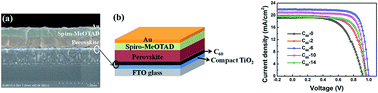
In perovskite solar cells (PSC), electron collection layers play a critical role in blocking holes and transporting electrons for high performances. In this study, a fullerene layer was introduced by a solution-process method between the TiO2 layer and CH3NH3PbI3 layer, which was synthesized via a low-pressure vapor assisted solution process. Both the fullerene and TiO2 layers acted as electron collection layers together. The results show that the electron collection bilayer dramatically enhances cell performance even with part of the fullerene dissolved in DMF solution. The optimized PSC can achieve a PCE of 16.58%, with a FF of 75.91% measured under reverse voltage scanning. For PSCs only using TiO2 as the collection layer, the average PCE and FF values are 10.2% and 58.6%, respectively. When fullerene was used as a single electron collection layer, the PCE is only 4.29%, because of the incomplete coverage of fullerene on the FTO substrate. Additionally, PSCs with fullerene interface layers showed far less hysteresis than reference cells without fullerene layers. Analysis of the equivalent circuit of devices and fluorescence lifetime measurements focusing on the CH3NH3PbI3 film with an electron extraction layer confirm that in our device configuration fullerene facilitates electron injection from CH3NH3PbI3 into the compact TiO2 layer.


Introduction

Since Miyasaka and co-workers introduced CH3NH3PbX3 (where X is I or Br) as sensitizers for liquid-electrolyte-based dye-sensitized solar cells between 2006 and 2009,1,2 organic/inorganic metal halide perovskite materials have come to the attention of photovoltaics researchers. After the introduction of the molecular solid state hole transporting material spiro-OMeTAD in solar cells,3 there was an explosion of interest in organic/inorganic hybrid perovskite materials. The study of these materials has become central to the field of thin-film photovoltaics, owing to these materials' unique photoelectrical properties, such as their direct bandgap nature, large absorption coefficient, ambipolar diffusion, long carrier diffusion length, small exciton binding energy, high dielectric constant, and high charge carrier mobility.4–10 The most striking development has been the rapid boost in the power conversion efficiency (PCE) of perovskite solar cells (PSCs), to more than 20% within 5 years.11 Two basic PSC device architectures (mesoporous and planar) have been reported.12 Planar-architecture PSCs can be further divided into n–i–p and p–i–n structures, in which the electron and hole collection layer, respectively, is adjacent to the transparent conducting electrode. A planar architecture potentially provides avenues for enhanced flexibility for device optimization, multi-junction construction, and investigation of the underlying device physics. Additionally, it has garnered great concerted research efforts in the areas of high-quality perovskite film fabrication and correct selection of carrier-selective transport layers to facilitate electron/hole extraction.

Interface modification layers are also crucial components for photogenerated charge extraction.13,14 A variety of routes have been proposed to facilitate electron/hole extraction through taking advantage of special materials such as fullerene, graphene, or core/shell metal nanoparticles.15–17 Three fullerene derivatives, phenyl-C61-butyric acid methyl ester (PCBM), indene-C60 bisadduct (IC60BA), and fullerene (C60), have been applied as electron extraction layers in PSCs.7,15,18 But they are usually applied between the perovskite layer and the metal back electrode, forming a p–i–n structure. When these facilitating electron extraction layers are used in n–i–p structure PSCs—besides their connection with the adjacent materials—their transmittance to visible light must also be considered. Fullerene-based interface layers were not widely used in n–i–p structure PSCs until a large enhancement of the PCE was demonstrated in CH3NH3PbI3−xClx PSCs with a TiO2 compact layer, which had been modified by a self-assembled C60 monolayer.14 However, the self-assembly procedure took more than 24 hours. In the subsequent synthesis of perovskite layers, dimethylformamide (DMF) was generally used as the solvent for dissolving PbI2. However, this method faced a serious problem that the C60 film may be also partially dissolved in DMF solution which may destroy the surface structure of C60 layer and deteriorate the electron-transporting properties.

Recently, Snaith's group19 and Fang's group20 reported that C60 layers could be alone directly deposited on the FTO substrates as electron collection layers in n–i–p structured PSCs. To avoid the meeting of DMF and C60, Snaith's group deposited PbI2 layer by vacuum thermal evaporation on the solution-processed C60 substrates.19 Alternatively, to obtain a relatively compact C60 layer to withstand the partial dissolution in DMF in the subsequent procedures, Fang's group prepared C60 layer by vacuum thermal evaporation.20 The vacuum thermal evaporation of C60 or PbI2 inevitably was an additional process for the general fabrication of PSCs. Anyway, solution-processed C60 layer intentionally followed by the subsequent DMF-processed PbI2 layer procedure was still an easy and feasible method. To simplify the fabrication process of PSCs, the metal C60/oxide electron collection bilayer would be an appropriate choice in the solution-phased process. On one hand, the C60 layer could improve the electron collection, on the other hand the metal oxide layer could remedy the imperfect coverage of the FTO substrate caused by the dissolution of C60 in DMF.

Besides the one-step or sequential deposition from solution methods for fabricating perovskite films, vapor deposition methods, including dual-source vacuum evaporation,21 low-pressure chemical vapor deposition,22 and vapor-assisted solution process (VASP),23 had also been developed to fabricate high-quality pinhole-free perovskite thin films. With respect to the conventional solution process, vapor deposition can not only avoid the solvation and dehydration processing or some undesirable structural transitions during solution process,24 but also effectively reduce the over-rapid intercalating reaction rate between PbI2 and CH3NH3I,22,25 which could result in optimized surface morphology of perovskite. In a typical VASP, CH3NH3I vapor reacts directly with the as-deposited PbI2 films, forming perovskite films with large grain sizes even up to micrometers,23–27 which generally differ from films prepared through traditional solution-based methods. Low-pressure VASP (LP-VASP), in which the gas–solid reaction takes place in low vacuum conditions,28 is a modified process which can also be used to fabricate efficient PSCs. Since the perovskite film morphologies produced by LP-VASP and all-solution processing are quite different, it is necessary to study whether C60 films are suitable for using as electron extraction layers in PSCs fabricated through LP-VASP. However, so far there are no reports on LP-VASP perovskite solar cells with C60 thin films as electron selective layers.

In this study, C60 layer was introduced by a solution-process method between the CH3NH3PbI3 layer and compact TiO2 layer in planar structured PSCs. Different from the previous studies, both C60 and TiO2 layers acted as the electron collection layers together, and CH3NH3PbI3 was synthesized via LP-VASP. Even if C60 dissolved in DMF, the synergetic effect of TiO2 and C60 layer offer the PSC excellent performance. By adjusting the C60 solution concentration, the optimized PSC can achieve a PCE of 16.58% with an FF of 75.91% measured under reverse voltage scanning operation. To the best of our knowledge, this PCE is among the highest record for the CH3NH3PbI3 PSC fabricated via VASP. Through equivalent circuit analysis of working devices and fluorescence lifetime measurements of CH3NH3PbI3 films with electron extraction layer, we have confirmed that in our device configuration C60 facilitates electron injection from CH3NH3PbI3 into the compact TiO2 layer. Therefore, in addition to the enhancement in PCE, insertion of a C60 layer also significantly reduces hysteresis compared with a reference cell without a C60 layer. Our results reveal that a solution-processed C60 layer can act as an efficient electron extraction layer in CH3NH3PbI3 PSCs fabricated via LP-VASP.

Experimental section

Materials

CH3NH3I (99.5%) and 2,2′,7,7′-tetrakis-(N,N-di-p-methoxyphenylamine)-9,9′-spirobifluorene (spiro-OMeTAD) (99.7%) were both purchased from Borun Chemicals (Ningbo, China). PbI2 (99%) and 1,2-dichlorobenzene (98%) were both purchased from Acros. C60 and N,N-dimethylformamide (DMF) were both purchased from Alfa Aesar. Isopropanol was purchased from J&K Scientific Co., Ltd. Tris(2-(1H-pyrazol-1-yl)-4-tert-butylpyridine)–cobalt(III)–tris(bis(trifluoromethylsulfonyl)imide) (FK209–cobalt(III)–TFSI) was purchased from MaterWin Chemicals (Shanghai, China). Bis(trifluoromethane)sulfonimide lithium salt and tert-butylpyridine (tBP) was purchased from Sigma-Aldrich. All chemicals were directly used without further purification. Glass substrates with a transparent fluorine doped tin oxide (FTO, thickness 2.2 mm, sheet resistance 15 Ω per square) layer were used for the PSCs.

Cell fabrication

The FTO glass substrates were first etched using Zn powder and 2 M HCl diluted in deionized (DI) water. Then the etched substrates were cleaned sequentially in a special detergent solution, DI water, and ethanol. After drying under clean dry air, the FTO glass substrates were annealed at 500 °C for 30 min in air to remove any remaining organic matter. Then, the c-TiO2 layer was deposited on the FTO glass substrates by spin-coating a precursor solution (titanium isopropoxide in anhydrous ethanol (0.254 M) with the addition of a 0.02 M HCl) at 3000 rpm for 30 s, followed by sintering at 500 °C for 30 min. The C60 layer was subsequently spin coated onto the TiO2 layer from a C60 1,2-dichlorobenzene solution at a speed of 1500 rpm, then dried at 60 °C for 2 min. Several different concentrations of the C60 1,2-dichlorobenzene solution, including 2, 6, 10, and 14 mg ml−1, were used to fabricate the various PSCs, which are referred to as C60-2, C60-6, C60-10, and C60-14. And the reference PSC without C60 layer was marked as C60-0.

After allowing the samples to cool, a solution of 462 mg ml−1 PbI2 in DMF was spin coated onto the FTO/c-TiO2/C60-x samples (x = 0, 2, 6, 10, and 14) at 3000 rpm for 30 s, and then dried at 70 °C for 30 min in a nitrogen-filled glovebox. CH3NH3I powder was evenly spread out around the PbI2 coated substrates in a Petri dish covered with a lid. The Petri dish was placed in a vacuum drying oven (10 kPa) set at 150 °C for 30 min. After this reaction process, the as-prepared perovskite films were first washed with isopropanol, then dried and annealed at 150 °C for 5 min in a nitrogen-filled glovebox.

For the hole transport layer, 20 μl of a spiro-OMeTAD mixed solution was spin coated onto each perovskite film at 4000 rpm for 30 s. The spiro-OMeTAD mixed solution was composed of 1 ml spiro-OMeTAD solution (72.3 mg of spiro-OMeTAD in 1 ml of chlorobenzene), 28.8 μl tBP, 17.5 μl Li–TFSI solution (520 mg of bis(trifluoromethane)sulfonimide lithium salt in 1 ml of acetonitrile) and 8 μl FK209–cobalt(III)–TFSI solution (300 mg of FK209–cobalt(III)–TFSI in 1 ml of acetonitrile). Finally, Au was thermally evaporated on top to form the back electrode (60 nm) at an atmospheric pressure of 4 × 10⁻⁴ Pa.

Characterization

Current density–voltage (JV) characteristic were measured with a Keithley 2400 source-meter together with a sunlight simulator (XES-300T1, SAN-EI Electric, AM 1.5), which was calibrated using a standard silicon reference cell. The solar cells were masked with a black aperture to define an active area of 0.09 cm2. Scanning electron microscopy (SEM) images were taken with a SU8010 SEM (Hitachi). X-ray diffraction (XRD) patters were measured with a Bruker X-ray diffractometer with a Cu-Kα radiation source. The 2θ diffraction angle was scanned from 10° to 80°, with a scanning speed of 3.5° per min. Atomic force microscopy (AFM) images were acquired in tapping mode with a 5500 AFM (Agilent Technologies). Incident photon-to-electron conversion efficiency (IPCE) was measured in air using a QE-R measurement system (Enli Technology). Time-resolved photoluminescence (TR-PL) spectra were collected by a transient state spectrophotometer (F900, Edinburgh Instruments). Samples were excited with a 660 nm pulsed diode laser with a repetition rate of 2.5 MHz and an excitation intensity of ∼14 nJ cm−2. Transmission spectra were measured with a UV-2450 spectrophotometer (Shimadzu) from 300 to 800 nm. Impedance spectra of the cells were obtained using an electrochemical workstation (Zahner) under AM1.5 illumination, at the positive bias voltages ranging from 0.5 to 1.0 V with an oscillating voltage of 10 mV and a frequency of 1 Hz to 1 MHz.

Results and discussion

Fig. 1(a) shows a representative SEM cross-sectional image of a PSC fabricated via LP-VASP with a C60 interlayer between the TiO2 and CH3NH3PbI3 layer. Several layers were deposited successively on top of the FTO glass substrate as follows: compact TiO2, C60, CH3NH3PbI3, spiro-OMeTAD, and Au. The total thickness of the cells was about 550 nm, most of which was owing to the CH3NH3PbI3 and spiro-OMeTAD layers. Since the TiO2 and C60 layers were ultra-thin, they were difficult to identify and distinguish from the other layers in the cross-sectional SEM image. A schematic diagram of the device architecture is shown in Fig. 1(b) for clarity. The area of the device stack that is the focus of this study is circled in the diagram. The energy band diagram of our PSCs were schematically shown in Fig. 1(c). The LUMO of C60 was reported as −4.1 eV,29 which matched with the conduction band level of the perovskite (−3.9 eV)20 and TiO2 (−4.2 eV).30 The valence band maximum of the perovskite (−5.4 eV) and HOMO of spiro-OMeTAD, and the Fermi level of FTO and Au electrodes were cited from the reported works.20 Finally, these band gap offsets between different layers made the photo-induced electrons and holes in the perovskite layer be extracted effectively by the electron collecting layer and hole collecting layer respectively.
image file: c6ra14372e-f1.tif
Fig. 1 (a) Cross-sectional SEM image, (b) schematic device architecture, and (c) schematic diagram of energy band of the FTO/TiO2/C60/CH3NH3PbI3/spiro-MeOTAD/Au cells.

The deposited C60 film may be partially dissolved during the deposition of the subsequent PbI2 layer, which is spin-coated from a DMF solution, and thus its hole-blocking properties may deteriorate.19 Therefore, a solution-processed C60 film alone may have difficulty shouldering the electron selecting function. Thus, in this study, C60 films were spin-coated from a dichlorobenzene solution on the top of TiO2-coated FTO glass substrates. TiO2 and C60 together constitute the electron selective layer. To characterize the surface morphology of the films beneath CH3NH3PbI3 layer by layer, SEM images of FTO, TiO2/FTO, and C60/TiO2/FTO (before and after processing with DMF) are shown in Fig. 2(a)–(d). The FTO surface (Fig. 2(a)) is so rough that its gain-boundaries visibly penetrate the thin TiO2 layer deposited on top (Fig. 2(b)). However, the root mean square roughness of the FTO substrate obtained from the AFM images (Fig. S1(a) and (b)) was reduced slightly by depositing the TiO2 layer. Pristine C60 films (Fig. 2(c)) visibly formed a complete coverage on top of the TiO2 layer, and caused an obvious reduction of the surface roughness (Fig. S1(c)). To clarify the effect of DMF on the morphology of the C60 film, we spin coated DMF on top of the C60/TiO2/FTO part of the device stack. As shown in Fig. 2(d), the morphology of C60 film changed a lot after the DMF process. The C60 layer took on a granular morphology, consistent with thousands of nanoparticles smaller than 50 nm covering the surface. Fig. 2(d) indicated that the C60 and c-TiO2 layers could still completely cover the surface of FTO although parts of C60 dissolve in DMF. This complete coverage provide PSCs an excellent hole-blocking properties. Accordingly, the roughness increased to a similar value to the sample prior to C60 deposition (Fig. S1(c) and (d)).


image file: c6ra14372e-f2.tif
Fig. 2 SEM images of (a) bare FTO substrate; (b) TiO2 layer on FTO substrate; and C60 layers on TiO2/FTO substrate (c) before and (d) after processed with DMF solution.

The DMF process also had an effect on the transmittance of the FTO/TiO2/C60 samples (Fig. S2). For every concentration of the C60 solution, the transmittance was enhanced after the DMF process. This observation is also evidence for the partial dissolution of C60 by DMF, which has been pointed out in previous research.19 Moreover, the partial dissolution can also be confirmed by the decrease in thicknesses of the C60-x (x = 2, 6, 10, and 14) layers after the DMF process. The thicknesses were obtained by measuring from the cross-sectional SEM images of FTO/TiO2/C60-x samples, as shown in Fig. S3. And the average thicknesses of the C60-x (x = 2, 6, 10, and 14) layers after blank solvent coating were 8.0, 15.6, 23.8 and 27.1 nm respectively. Due to spin-coating PbI2 layer from a DMF solution on C60 layers in our experiments, we measured the transmittances of the FTO/TiO2/C60 samples after the DMF processes (Fig. 3). As we increased the concentration of the C60 solution, the transmittances of the samples decreased, particularly for the wavelengths shorter than 550 nm. Thus, the addition of C60 on top of the TiO2 layer was bound to cause some loss of the visible light incident on the perovskite layer.


image file: c6ra14372e-f3.tif
Fig. 3 Transmission spectra of FTO substrate, TiO2 layer on FTO substrate, and C60 layers on TiO2/FTO substrate spin-coated from different solution concentrations after spin-coating DMF solution on top.

The effects of the C60 layer on the microscopic morphologies and crystal structures of both PbI2 and CH3NH3PbI3 films have also been analyzed. Porous PbI2 films were formed on both FTO/TiO2 (Fig. 4(a)) and FTO/TiO2/C60 samples (Fig. 4(b)). However, the film deposited on the FTO/TiO2/C60 sample possessed greater porosity and roughness (Fig. S4(a) and (b)) than the film deposited on FTO/TiO2. The XRD patterns shown in Fig. S5(a) exhibited the hexagonal 2H polytype crystallization of PbI2 for all the samples prepared with different C60 solution concentrations. The strong diffraction peak at 12.6° corresponds to its (001) lattice plane.31 The surface morphologies of CH3NH3PbI3 on FTO/TiO2 and FTO/TiO2/C60 were characterized by SEM as shown in Fig. 4(c) and (d), respectively. In both cases, the CH3NH3PbI3 films showed full coverage and a large-sized grain structure. For the films deposited on FTO/TiO2, numerous smaller grains could be observed in the gaps between the larger grains. Although the largest grain size of the film deposited on FTO/TiO2/C60 was smaller than that of the film deposited on FTO/TiO2, the distribution of the grain size was narrower in the former film compared with the latter one. Analysis of the XRD spectra shown in Fig. S5(b) revealed no significant difference in perovskite crystallization among all the CH3NH3PbI3 films prepared with the various C60 solution concentrations and deposited onto the various materials. The sharp diffraction peaks at 14.1°, 24.5°, 28.4°, and 31.8°, were assigned as the (100), (111), (200), and (210) lattice planes, respectively, of a cubic perovskite structure.4 The peak at 12.6° was ascribed to the PbI2 residual for all the samples.


image file: c6ra14372e-f4.tif
Fig. 4 SEM images of PbI2 films on (a) FTO and (b) FTO/TiO2/C60-6; and CH3NH3PbI3 films on (c) FTO/TiO2 and (d) FTO/TiO2/C60-6.

The JV curves of the PSCs with and without a C60 interface layer prepared with different solution concentrations measured under the reverse voltage scanning voltages are shown in Fig. 5. The curves in the figure correspond to best-performing PSCs of each device set. The average statistical values of each device set (Fig. 6(a)) display the same dependency on the C60 solution concentration as the best-performing samples. The cell performances improved when a C60 interface layer was used. The PSC without the C60 interface layer only achieved a PCE of 10.61%, with an open circuit voltage (Voc) of 0.93 V, a short circuit current (Jsc) of 18.77 mA cm−2, and a FF of 60.82%. The PCE of the PSCs with C60 interface layers first increased then decreased as the concentration of the C60 solution increased. The cell prepared with 6 mg ml−1 C60 concentration had the best PCE of all the cells we studied. Specifically, this cell attained a maximum PCE of 16.58%, with a Voc of 1.00 V, a Jsc of 21.92 mA cm−2, and a FF of 75.91%. The photovoltaic parameters of the other PSCs shown in Fig. 5 are summarized in Table 1. Moreover, box plots of PCE, Voc, Jsc, and FF of all the PSCs with varying C60 solution concentrations are shown in Fig. 6. The photovoltaic properties of the various cells described above show that improvements in Voc, Jsc, and FF all contribute to the enhanced PSC performance achieved by the insertion of the C60 layer. SEM images of C60/FTO before and after processed with DMF were shown in Fig. S6. Before processing with DMF, the C60 layer could completely cover the FTO surface (Fig. S6(a)). However, Fig. S6(b) showed that part of FTO surface exposed outside after processed with DMF (indicated by the red circle) because the dissolution of C60 in DMF. To understand the effect of c-TiO2 layer on the performance of PSCs, the JV curves of the PSCs with and without the c-TiO2 layer (with the C60 concentration of 6 mg ml−1) measured under reverse voltage scanning voltage were shown in Fig. S7. The cell without the c-TiO2 layer just attained a maximum PCE of 4.29%, with a Voc of 0.62 V, a Jsc of 19.57 mA cm−2, and a FF of 35.42%. The performance decay of the PSCs without c-TiO2 layer was due to the lack of the effective barrier, and the recombination of carriers was enhanced.


image file: c6ra14372e-f5.tif
Fig. 5 JV curves of the PSCs without and with C60 interface layers, which were prepared with different solution concentrations. Only the curves from the best performing PSCs of each set measured under the reverse voltage scanning are shown.

image file: c6ra14372e-f6.tif
Fig. 6 Statistical results for (a) PCE, (b) Voc, (c) Jsc and (d) FF values of PSCs with C60 interface layers, which were prepared with different solution concentrations. Twenty samples of each device set were measured.
Table 1 Photovoltaic parameters of PSCs with and without C60 interface layers, which were prepared with different solution concentrations
Concentration of C60 (mg ml−1) Voc (V) Jsc (mA cm−2) FF (%) η (reverse) (%) η (forward) (%)
0 0.93 18.77 60.82 10.61 5.48
2 0.97 19.79 64.79 12.48 7.32
6 1.00 21.92 75.91 16.58 13.28
10 0.97 20.92 74.81 15.12 12.75
14 0.95 19.59 72.16 13.48 12.19


Equivalent circuit analysis was carried out to extract more information about the cells from their JV curves. Solar cells are roughly equivalent to a parallel circuit consisting of a current source and a diode. The output currents density (J) of the cells can be described as,32

 
image file: c6ra14372e-t1.tif(1)
where J0 is the reverse saturated current density, Jsc is the measured short-circuit current density, Rs and Rsh are the series and shunt resistance, respectively, A is the ideality factor of a heterojunction, K is the Boltzmann constant, T is the absolute temperature, q is the elementary charge, and V is the direct-circuit bias voltage applied to the cell. When RsRsh, eqn (1) can be expressed as
 
image file: c6ra14372e-t2.tif(2)

Fig. 7(a) gives the plots of dV/dJ vs. (J + Jsc)−1 and the linear fitting curves of the PSCs with different concentration of C60 according to eqn (2). It can be found that the relationship between dV/dJ and (J + Jsc)−1 becomes more linear as the C60 solution concentration increases. The slope and intercept of the linear fitting results can be obtained by calculating the ideality factor and series resistance, respectively.


image file: c6ra14372e-f7.tif
Fig. 7 (a) Plots of (dV/dJ) vs. (J + Jsc)−1 for the best performing cells under illumination (linear fitting curves also are shown). (b) Series resistances (Rs) and ideality factors (A) derived from fitting curves in (a).

The values of Rs and A for different C60 solution concentrations are shown in Fig. 7(b). When C60 interface layers were used in the PSCs, Rs decreased from 3.51 Ω cm2 to the lowest value of 0.69 Ω cm2; additionally, A decreased from 4.35 to the lowest value of 2.31. The decrease in Rs induced by the insertion of the C60 interface layer can be attributed not only to a reduction of charge carrier recombination at the compact TiO2/CH3NH3PbI3 interfaces in the cells, but also to good electron mobility of C60.20,33 For a well behaved single heterojunction solar cell, the ideality factor is typically in the range of 1 < A < 2.34 The two boundary values of 1 and 2 represent two extreme cases in which the diode current is dominated by carrier diffusion or recombination, respectively, for low charge carrier injection.35 Because our PSCs are much more complex than the single heterojunction solar cells, the ideality factors in our study were all above 2. Nevertheless, the addition of the C60 layer in the PSCs caused a significant reduction of the ideality factors, and they were much closer to the ideality factors of ideal diodes than the ones of the PSC without the C60 interface layer. When the C60 solution concentration was 10 mg ml−1, the ideality factor achieved was 2.31—the smallest value we measured in our studies. However, it cannot be ignored that the addition of the C60 layers inevitably introduces their own intrinsic resistance into the cells. When the increase in the intrinsic resistance of the C60 layer offsets the decrease in the carrier recombination at the original interface between the c-TiO2 and CH3NH3PbI3 layers, the series resistance starts to increase. Owing to the above mentioned two effects of adding the C60 layer, the optimized solution concentration in our study was 6 mg ml−1.

An equivalent circuit was used to analyze the dark condition JV curves (Fig. S8). Similar to the results under illumination discussed above, the C60-6 sample had the smallest Rs in our study. The ideality factor decreased from its original value of 3.23 to 2.22. We found smaller differences in ideality factors taken in dark and under illumination for the PSCs with a C60 layer compared with the PSCs without a C60 layer. The change in a cell's ideality factor under illumination compared with under dark conditions reflects the changes induced by the illumination of the internal functional layers of the cell. Thus, it can be concluded that C60 interface layers play a role in stabilizing the chemical and physical properties of the adjacent materials in the cell.

To study the spectral response of the devices, we measured the IPCE spectra of the best-performing PSC with and without a C60 interface layer (Fig. 8). The integrated photocurrent obtained from the IPCE curve of the cell with a C60 layer was 20.32 mA cm−2. This value is slightly lower than the Jsc obtained from the JV curve under both forward and reverse bias voltage scanning. We attribute this to chemical and physical changes that affect the performance of PSCs, which are affected by different historical processes in the measurement. Though the transmittance of the samples was slightly reduced in the short wavelength range by the C60 layers, the corresponding IPCE spectrum does not show a reduction in this wavelength range. The integrated photocurrent obtained from the IPCE curve of the cell without an interface layer was only 15.53 mA cm−2. The high IPCE values of PSCs with C60 layers can be attributed to the strong absorption of visible light by the CH3NH3PbI3 film and effective electron–hole separation and collection at the interfaces.


image file: c6ra14372e-f8.tif
Fig. 8 IPCE spectra of the best-performing cells with and without a C60 interface layer.

To obtain more in-depth information, the photoluminescence lifetime of the CH3NH3PbI3/C60-x/TiO2 (x = 0, 2, 6, 10, and 14) samples are evaluated by TR-PL and the results are shown in Fig. 9(a). Biexponential decay functions were used to fit the decay curves, which contain a fast and a slow decay component. The parameters resulting from the fitting are summarized in Table 2. When the perovskite film is in the presence of a quenching layer, the quencher mainly contributes to the fast decay process. The t2 value, which represents the fast decay component of the sample, was 0.97 ns for the sample without the C60 layer. In contrast, when CH3NH3PbI3 films were interfaced with C60 layers, all t2 values dropped to 0.40 or 0.39 ns. The whole decay process also includes the radiative recombination within the perovskite layer. A calculated average lifetime (tave), which takes into account both time constants as well as their weighting, was used to evaluate the whole lifetime of the film. The CH3NH3PbI3/TiO2 sample had much longer carrier lifetimes (24.33 ns) than the other samples with C60 interface layers. Thus, the results demonstrate that C60 plays an important role in effectively quenching photoinduced carriers generated in the perovskite absorbers. Although the PSCs assembled with CH3NH3PbI3/C60-6/TiO2 showed the best performance in our studies, the average lifetime of CH3NH3PbI3/C60-6/TiO2 sample was longer than that of the CH3NH3PbI3/C60-10/TiO2 and CH3NH3PbI3/C60-14/TiO2 sample. In this measurement, the laser beam illuminated the samples from the CH3NH3PbI3 side. However, in the real JV measurements of our solar cells, light is incident from the FTO side; it penetrates through TiO2 first, then C60, and is finally absorbed by the CH3NH3PbI3 layer. Additionally, transmission spectra (Fig. 3) showed that the loss of incident light at wavelength shorter than 550 nm increased for higher C60 solution concentrations. Thus, the shortest average lifetime for the monochromatic light here is not necessarily representative of the working PSC device with the highest PCE.


image file: c6ra14372e-f9.tif
Fig. 9 (a) TR-PL spectra for quartz/TiO2/C60-x/CH3NH3PbI3 samples after excitation at 635 nm. Normalization was performed with respect to the data for the x = 0 sample. (b) Charge transfer resistance resulting from impedance spectrometry measurements fitted for different applied biases under illumination (inset: Nyquist plots of the cells at 900 mV) of the cells with and without a C60-6 layer, respectively.
Table 2 Time parameters derived from the fitting results of the transient TR-PL decay curves shown in Fig. 9
  Sample
TiO2/C60-x/CH3NH3PbI3 (x=)
0 2 6 10 14
t1 Value (ns) 25.65 35.38 34.11 17.23 27.24
Rel. (%) 94.64 24.65 11.37 8.65 13.83
t2 Value (ns) 0.97 0.40 0.40 0.39 0.40
Rel. (%) 5.36 75.35 88.63 91.35 86.17
tave Value (ns) 24.33 9.02 4.23 1.85 4.11


Moreover, impedance spectrometry was used to study the charge recombination in PSCs with and without a C60 interface layer under illumination. Inset in Fig. 9(b) plots characteristic Nyquist patterns obtained for both cells at applied voltage of 0.9 V in the working conditions. Semicircles can be observed for both cells, and they were fitted with a resistance-constant phase element model. Thus, the values of charge transfer resistance (Rct) were obtained, which related the charge transfer within the whole cells. As can be seen in Fig. 9(b), at different bias voltages, all the Rct values of the PCS with a C60-6 interface layer were obviously larger than that of the PSC without C60 layer. It indicated that the recombination of the photo-induced carriers in planar PSCs has been significantly suppressed by inserting a C60 layer between the compact TiO2 and CH3NH3PbI3 layers. The result agrees with other results obtained by the equivalent circuit and TR-PL analysis discussed above.36

Hysteresis effects of the PSCs have also been reduced by using the C60 interface layers. Fig. 10 shows the JV curves of the PSCs with a C60 interface layer (prepared from a 6 mg ml−1 solution) and without one, measured in forward and reverse voltage scanning at the same scan rate. Both two kinds of cells had lower PCE values under forward voltage scanning than under reverse voltage scanning. However, by comparing the differences between the PCE values obtained under forward and reverse voltage scanning, it can be confirmed that the PSC with the C60 interface layer exhibit much less hysteresis than the cells without the interface layer. Additionally, the PCEs obtained under reverse voltage scanning conditions are summarized in Table 1 for every kind of cell in our study. Two probable reasons are considered attributing to the less hysteresis in the PSC with the C60 interface layer. Firstly, it had been confirmed that capacitive charge would tend to be stored in the perovskite films composed of smaller CH3NH3PbI3 crystals, which released as crystal size increased.35 The hysteresis was alleviated as crystal size increased.35 As shown in Fig. 4(c) and (d), compared with the perovskite film on FTO/TiO2/C60, there are much more small grains in the film deposited on FTO/TiO2 substrate. The numerous small CH3NH3PbI3 grains could store more capacitive charges and thus result in more serious hysteresis. Secondly, it has been previously suggested that defects near the surface of the material or specifically generated interface states are possible causes for the anomalous hysteresis in PSCs.37 The reduced hysteresis of the PSCs in this study can be attributed to the C60 induced passivation of the TiO2/CH3NH3PbI3 interface. Previous research has demonstrated that fullerenes can effectively passivate grain boundaries, reduce the density of trap states and non-radiative recombination, thus further reduce or even eliminate hysteresis for PSCs.14,20,38–40


image file: c6ra14372e-f10.tif
Fig. 10 JV curves of the PSCs with and without C60 interface layers, which were prepared with a solution concentration of 6 mg ml−1. PSCs were measured under both forward and reverse voltage scanning.

To determine the steady-state performance and probe the repeatability of the cells, current densities of the PSC with C60-6 as interface layers have be studied as a function of time under persistent illumination (Fig. 11(a)) and pulse type illumination (Fig. 11(b)) generated by a solar simulator. Moreover, the measurements were carried out under two conditions, namely under the forward voltage scanning of 0 V and 0.82 V which corresponds to the maximum power points of the cells. The current densities at these two cases marked as Jsc and JPmax, respectively, and are shown in Fig. 11. As shown in Fig. 11(a), immediately after light turn-on, there was an initial fast drop and a slow and slight decrease in the Jsc. The proportional decrease in Jsc compared with the entire illumination of 150 s was only about 2%. After an initial slow increase for about 10 s, JPmax, settled in the range of 19.2–19.5 mA cm−2, which is between the values obtained from forward and reverse voltage scanning. As shown in Fig. 11(b), five cycles of pulse type illumination demonstrated good repeatability of both Jsc and JPmax for the PSCs.


image file: c6ra14372e-f11.tif
Fig. 11 Dynamic response of current density for FTO/TiO2/C60-6/CH3NH3PbI3/spiro-MeOTAD/Au cells at bias voltages of 0 and 0.82 V, which represent the voltage for Jsc and JPmax, respectively. (a) Under continuous illumination after being kept in the dark for 10 s, and (b) after repetitive illumination pulses with both a duration and an interval of 10 s.

We additionally checked whether the prepared FTO/TiO2/C60 modified substrates could be used to fabricate PSCs with a high PCE via an all-solution process. To test this, CH3NH3I in isopropanol (8.0 mg ml−1) was used to react with PbI2 film deposited by spin-coating and a following annealing at 70 °C for 30 min. The best-performing JV curves for this kind of PSC are shown in Fig. S9. Obviously, the PCEs under both forward and reverse voltage scanning were lower than those of the cells fabricated via LP-VASP.

Conclusions

In conclusion, we have demonstrated a solution-processed C60 layer can be used as an interface layer between a c-TiO2 layer and a CH3NH3PbI3 layer synthesized via LP-VASP. The C60/c-TiO2 bilayer can act as an excellent electron collection layer to enhance cell performance dramatically.

By adjusting the C60 solution concentration, the optimized PSC can achieve a PCE of 16.58% with an FF of 75.91% measured under reverse voltage scanning operation. Without C60 interface layers, the PSCs possess average PCE, FF, Jsc, and Voc values of 10.2%, 58.6%, 18.6 mA cm−2, and 0.93 V, respectively, which were increased to 16.1%, 73.4%, 22.2 mA cm−2, and 0.99 V by inserting the C60 interface layer prepared with a solution concentration of 6 mg ml−1. While C60 was alone used as the electron collection layer, the dissolution of C60 in DMF destroyed the structure of C60 layer and decayed the performance of cell. Additionally, PSCs with C60/TiO2 layers showed far less hysteresis than the reference cells without C60 layers. While adding the C60 layer caused some loss of light incident on the perovskite layer, it still had a positive impact in the following two ways: first, by analyzing the JV curves with equivalent circuits, we confirmed that the C60 interface layer reduces the series resistance of the cells and optimizes the ideality factor, so that the ideality factor values are closer to those for a well behaved single heterojunction diode. Second, the results of the TR-PL measurements showed that fluorescence lifetimes of the perovskite films adjacent to C60 layers were much shorter than the lifetimes of perovskite films directly adjacent to c-TiO2 layers; this indicates fast extraction of photoinduced electrons by the C60 interface layer. Our results suggest that solution-processed C60 layers can act as an efficient electron collection enhancer in PSCs prepared via LP-VASP, which is an important step towards fabricating high performing PSCs with large areas.

Acknowledgements

This work was supported by the National High Technology Research and Development Program of China (863 Program) (No. 2015AA050602), the National Natural Science Foundation of China (No. 51372083), and the Fundamental Research Funds for the Central Universities (No. 2014ZZD07, 2015ZD11).

References

  1. A. Kojima, K. Teshima, Y. Shirai and T. Miyasaka, 210th ECS Meeting, Cancun, Mexico, Oct. 29–Nov. 3, 2006 Search PubMed.
  2. A. Kojima, K. Teshima, Y. Shirai and T. Miyasaka, J. Am. Chem. Soc., 2009, 131, 6050–6051 CrossRef CAS PubMed.
  3. H. S. Kim, C. R. Lee, J. H. Im, K. B. Lee, T. Moehl, A. Marchioro, S. J. Moon, R. Humphry-Baker, J. H. Yum, J. E. Moser, M. Grätzel and N. G. Park, Sci. Rep., 2012, 2, 591 Search PubMed.
  4. T. Baikie, Y. Fang, J. M. Kadro, M. Schreyer, F. Wei, S. G. Mhaisalkar, M. Grätzel and T. J. White, J. Mater. Chem. A, 2013, 1, 5628–5641 CAS.
  5. H. J. Snaith, J. Phys. Chem. Lett., 2013, 4, 3623–3630 CrossRef CAS.
  6. J. H. Heo, S. H. Im, J. H. Noh, T. N. Mandal, C. S. Lim, J. A. Chang, Y. H. Lee, H. J. Kim, A. Sarkar, M. K. Nazeeruddin, M. Grätzel and S. I. Seok, Nat. Photonics, 2013, 7, 487 CrossRef.
  7. S. D. Stranks, G. E. Eperon, G. Grancini, C. Menelaou, M. J. P. Alcocer, T. Leijtens, L. M. Herz, A. Petrozza and H. J. Snaith, Science, 2013, 342, 341–344 CrossRef CAS PubMed.
  8. D. Q. Bi, S. J. Moon, L. Haggman, G. Boschloo, L. Yang, E. M. J. Johansson, M. K. Nazeeruddin, M. Grätzel and A. Hagfeldt, RSC Adv., 2013, 3, 18762–18766 RSC.
  9. E. J. Juarez-Perez, R. S. Sanchez, L. Badia, G. Garcia-Belmonte, Y. S. Kang, I. Mora-Sero and J. Bisquert, J. Phys. Chem. Lett., 2014, 5, 2390–2394 CrossRef CAS PubMed.
  10. S. Gamliel and L. Etgar, RSC Adv., 2014, 4, 29012–29021 RSC.
  11. National Renewable Energy Laboratory, Best Research-Cell Efficiencies, 2015, http://www.nrel.gov/ncpv/images/efficiency_chart.jpg Search PubMed.
  12. M. Grätzel, Nat. Mater., 2014, 13, 838–842 CrossRef PubMed.
  13. C. Tao, S. Neutzner, L. Colella, S. Marras, A. R. S. Kandada, M. Gandini, M. D. Bastiani, G. Pace, L. Manna, M. Caironi, C. Bertarelliac and A. Petrozza, Energy Environ. Sci., 2015, 8, 2365–2370 CAS.
  14. K. Wojciechowski, S. D. Stranks, A. Abate, G. Sadoughi, A. Sadhanala, N. Kopidakis, G. Rumbles, C. Z. Li, R. H. Friend, A. K. Jen and H. J. Snaith, ACS Nano, 2014, 8, 12701–12709 CrossRef CAS PubMed.
  15. J. Y. Jeng, Y. F. Chiang, M. H. Lee, S. R. Peng, T. F. Guo, P. Chen and T. C. Wen, Adv. Mater., 2013, 25, 3727–3732 CrossRef CAS PubMed.
  16. J. T. W. Wang, J. M. Ball, E. M. Barea, A. Abate, J. A. Alexander-Webber, J. Huang, M. Saliba, I. Mora-Sero, J. Bisquert, H. J. Snaith and R. J. Nicholas, Nano Lett., 2014, 14, 724–730 CrossRef CAS PubMed.
  17. W. Zhang, M. Saliba, S. D. Stranks, Y. Sun, X. Shi, U. Wiesner and H. J. Snaith, Nano Lett., 2013, 13, 4505–4510 CrossRef CAS PubMed.
  18. G. Xing, N. Mathews, S. Sun, S. S. Lim, Y. M. Lam, M. Grätzel, S. Mhaisalkar and T. C. Sum, Science, 2013, 342, 344–347 CrossRef CAS PubMed.
  19. K. Wojciechowski, T. Leijtens, S. Siprova, C. Schlueter, M. T. Hörantner, J. T. W. Wang, C. Z. Li, A. K. Y. Jen, T. L. Lee and H. J. Snaith, J. Phys. Chem. Lett., 2015, 6, 2399–2405 CrossRef CAS PubMed.
  20. W. Ke, D. Zhao, C. R. Grice, A. J. Cimaroli, J. Ge, H. Tao, H. Lei, G. Fang and Y. Yan, J. Mater. Chem. A, 2015, 3, 17971–17976 CAS.
  21. M. Liu, M. B. Johnston and H. J. Snaith, Nature, 2013, 501, 395–398 CrossRef CAS PubMed.
  22. P. Luo, Z. Liu, W. Xia, C. Yuan, J. Cheng and Y. Lu, ACS Appl. Mater. Interfaces, 2015, 7, 2708–2714 CAS.
  23. Q. Chen, H. Zhou, Z. Hong, S. Luo, H. S. Duan, H. H. Wang, Y. Liu, G. Li and Y. Yang, J. Am. Chem. Soc., 2014, 136, 622–625 CrossRef CAS PubMed.
  24. H. Feng, C. C. Stoumpos, L. Zhao, R. P. H. Chang and M. G. Kanatzidis, J. Am. Chem. Soc., 2014, 136, 16411–16419 CrossRef PubMed.
  25. T. Du, N. Wang, H. J. Chen, H. Lin and H. C. He, ACS Appl. Mater. Interfaces, 2015, 7, 3382–3388 CAS.
  26. C. Liu, J. D. Fan, X. Zhang, Y. J. Shen, L. Yang and Y. H. Mai, ACS Appl. Mater. Interfaces, 2015, 7, 9066–9071 CAS.
  27. Q. Chen, H. Zhou, T. B. Song, S. Luo, Z. Hong, H. S. Duan, L. Dou, Y. Liu and Y. Yang, Nano Lett., 2014, 14, 4158–4163 CrossRef CAS PubMed.
  28. Y. Li, J. K. Cooper, R. Buonsanti, C. Giannini, Y. Liu, F. M. Toma and I. D. Sharp, J. Phys. Chem. Lett., 2015, 6, 493–499 CrossRef CAS PubMed.
  29. W. C. Lai, K. W. Lin, T. F. Guo, P. Chen and Y. T. Wang, Appl. Phys. Lett., 2015, 107, 253301 CrossRef.
  30. G. Yang, H. Tao, P. Qin, W. Ke and G. Fang, J. Mater. Chem. A, 2016, 4, 3970–3990 CAS.
  31. D. H. Cao, C. C. Stoumpos, O. K. Farha, J. T. Hupp and M. G. Kanatzidis, J. Am. Chem. Soc., 2015, 137, 7843–7850 CrossRef CAS PubMed.
  32. J. J. Shi, J. Dong, S. T. Lv, Y. Z. Xu, L. F. Zhu, J. Y. Xiao, X. Xu, H. J. Wu, D. M. Li, Y. H. Luo and Q. B. Meng, Appl. Phys. Lett., 2014, 104, 063901 CrossRef.
  33. P. W. Liang, C. C. Chueh, X. K. Xin, F. Zuo, S. T. Williams, C. Y. Liao and A. K. Y. Jen, Adv. Energy Mater., 2015, 5, 140233221 Search PubMed.
  34. S. M. Sze and K. K. Ng, Physics of Semiconductor Devices, 3rd edn, 2006 Search PubMed.
  35. H. S. Kim and N. G. Park, J. Phys. Chem. Lett., 2014, 5, 2927–2934 CrossRef CAS PubMed.
  36. X. Xu, H. Y. Zhang, J. J. Shi, J. Dong, Y. H. Luo, D. M. Li and Q. B. Meng, J. Mater. Chem. A, 2015, 3, 19288–19293 CAS.
  37. H. J. Snaith, A. Abate, J. M. Ball, G. E. Eperon, T. Leijtens, N. K. Noel, S. D. Stranks, J. T. W. Wang, K. Wojciechowski and W. Zhang, J. Phys. Chem. Lett., 2014, 5, 1511–1515 CrossRef CAS PubMed.
  38. Y. C. Shao, Z. G. Xiao, C. Bi, Y. B. Yuan and J. S. Huang, Nat. Commun., 2014, 5, 5784 CrossRef CAS PubMed.
  39. A. Abrusci, S. D. Stranks, P. Docampo, H. L. Yip, A. K. Jen and H. J. Snaith, Nano Lett., 2013, 13, 3124–3128 CrossRef CAS PubMed.
  40. J. Xu, A. Buin, A. H. Ip, W. Li, O. Voznyy, R. Comin, M. Yuan, S. Jeon, Z. Ning, J. J. McDowell, P. Kanjanaboos, J. P. Sun, X. Lan, L. N. Quan, D. H. Kim, I. G. Hill, P. Maksymovych and E. H. Sargent, Nat. Commun., 2015, 6, 7081 CrossRef CAS PubMed.

Footnote

Electronic supplementary information (ESI) available. See DOI: 10.1039/c6ra14372e

This journal is © The Royal Society of Chemistry 2016