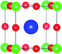
Potential thermoelectric materials CsMI3 (M = Sn and Pb) in perovskite structures from first-principles calculations

San-Dong Guo* and Jian-Li Wang
Department of Physics, School of Sciences, China University of Mining and Technology, Xuzhou 221116, Jiangsu, China. E-mail: guosd@cumt.edu.cn

Received 31st May 2016 , Accepted 11th October 2016

First published on 13th October 2016


Abstract

The thermoelectric properties of halide perovskites CsMI3 (M = Sn and Pb) are investigated from a combination of first-principles calculations and semiclassical Boltzmann transport theory by considering both the electron and phonon transport. The electronic part is performed using a modified Becke and Johnson (mBJ) exchange potential, including spin–orbit coupling (SOC), while the phonon part is computed using generalized gradient approximation (GGA). It is found that SOC has remarkable detrimental effect on the n-type power factor, while it has a negligible influence on p-type doping, which can be explained by considering the effect of SOC on the conduction and valence bands. The calculated results show exceptionally low lattice thermal conductivities in CsSnI3 and CsPbI3, and the corresponding room-temperature lattice thermal conductivity is 0.54 W m−1 K−1 and 0.25 W m−1 K−1, which suggests that they may be potential thermoelectric materials. At 1000 K, the maximal figure of merit ZT is up to 0.63 and 0.64 for CsSnI3 and CsPbI3 with scattering time τ = 10−14 s, and the peak ZT is 0.49 and 0.41 with τ = 10−15 s. These results lead us to believe that CsMI3 (M = Sn and Pb) in perovskite structures may be potential thermoelectric materials.


I. Introduction

Thermoelectric materials enable the direct conversion from heat to electricity, which may make an essential contribution to the energy crisis.1,2 A good thermoelectric material should have high dimensionless figure of merit ZT = S2σT/(κe + κL), where S, σ, T, κe and κL are the Seebeck coefficient, electrical conductivity, absolute temperature, the electronic and lattice thermal conductivities, respectively. A high ZT material requires a high power factor (S2σ) and low thermal conductivity (κ = κe + κL). They generally influence each other, and a counteracting relationship between the electrical conductivity and thermal conductivity or Seebeck coefficient is often found. Excellent classic thermoelectric materials include bismuth–tellurium systems,3,4 silicon–germanium alloys,5,6 lead chalcogenides7,8 and skutterudites.9,10 For thermoelectric research, searching for potential high ZT materials with a classic common lattice structure, like a perovskite structure, is interesting and challenging.

The cubic perovskite structure SrTiO3 has attracted growing attention for thermoelectric power generation.11 The ZT value of undoped SrTiO3 is less than 0.5 due to its high thermal conductivity,12 which can be reduced by introducing point defects.13,14 Searching other perovskites for more efficient thermoelectric applications is imperative and fruitful. The AMX3 perovskites (A = Cs, CH3NH3; M = Sn, Pb; X = halide) have recently attracted a great deal of attention for solar cell designs, which can realize up to 15% energy conversion efficiencies.15–18 A fair amount of theoretical works have been performed to investigate their electronic structures, phonons and optical properties.19–24 The CsMI3 (M = Sn and Pb) under reasonable hydrostatic pressure can turn into three-dimensional topological insulators, which has been predicted by first-principles calculations.25,26

Here, we report on the thermoelectric properties of cubic CsMI3 (M = Sn and Pb) in perovskite structures from a combination of first-principles calculations and semiclassical Boltzmann transport theory. The spin–orbit coupling (SOC) can produce obvious effects on the power factor of many thermoelectric materials,27–34 so the SOC is included in our calculations of the electronic part. The calculated results show that SOC has a notably reduced influence on the n-type power factor. It is noteworthy that ultralow lattice thermal conductivities are attained for CsMI3 (M = Sn and Pb), and the corresponding lattice thermal conductivities at 300 K are 0.54 W m−1 K−1 and 0.25 W m−1 K−1, which is comparable with the lattice thermal conductivity of 0.23 W m−1 K−1 in SnSe with an unprecedented ZT of 2.6 at 923 K.35 Finally, the dimensionless thermoelectric figure of merit ZT is calculated with τ = 10−14 s or τ = 10−15 s, and can reach about 0.6 or 0.4 at high temperature with optimized doping.

The rest of the paper is organized as follows. In the next section, we shall describe computational details. In the third section, we shall present the electronic structures and thermoelectric properties of CsMI3 (M = Sn and Pb). Finally, we shall give our discussions and conclusion in the fourth section.

II. Computational details

The electronic structures of CsMI3 (M = Sn and Pb) are modelled using a full-potential linearized augmented-plane-waves method within the density functional theory (DFT),36 as implemented in the WIEN2k package.37 We employ Tran and Blaha's mBJ exchange potential plus local-density approximation (LDA) correlation potential for the exchange–correlation potential,38 which has been known to produce more accurate band gaps than LDA and GGA for these materials.39 Moreover, the computational time is nearly the same as those for LDA or GGA. The SOC was included self-consistently40–43 due to containing heavy elements, which leads to band splitting, and produces important effects on the power factor. We use 5000 k-points in the first Brillouin zone for the self-consistent calculation, make harmonic expansion up to lmax = 10 in each of the atomic spheres, and set Rmt × kmax = 8. The self-consistent calculations are considered to be converged when the integration of the absolute charge-density difference between the input and output electron density is less than 0.0001|e| per formula unit, where e is the electron charge. Transport calculations, including Seebeck coefficient, electrical conductivity and electronic thermal conductivity, are performed through solving Boltzmann transport equations within the constant scattering time approximation (CSTA) as implemented in BoltzTrap,44 and reliable results have been obtained for several materials.45–47 To obtain accurate transport coefficients, we use 140[thin space (1/6-em)]000 k-points in the first Brillouin zone for the energy band calculation. The lattice thermal conductivities are calculated within the linearized phonon Boltzmann equation by using Phono3py + VASP codes.48–51 For the third-order force constants, 2 × 2 × 2 supercells are built, and reciprocal spaces of the supercells are sampled by 3 × 3 × 3 meshes. To compute lattice thermal conductivities, the reciprocal spaces of the primitive cells are sampled using the 20 × 20 × 20 meshes.

III. Main calculated results and analysis

CsMI3 (M = Sn and Pb) belong to the family of perovskite semiconductors, which consists of a network of corner-sharing MI6 octahedra. The perovskites undergo a series of structural transitions from high temperature to low temperature due to the rotations and rearrangements of the MI6 octahedra; they change from the cubic phase to the tetragonal phase, and then to the orthorhombic phase. To attain the lattice thermal conductivity relatively easily (calculating lattice thermal conductivity is very time consuming, especially for a low-symmetry structure), we investigate cubic CsMI3 (M = Sn and Pb), and the schematic crystal structure is shown in Fig. 1. Based on the experimental structures, the electronic structures of CsMI3 (M = Sn and Pb) are investigated using mBJ and mBJ + SOC, and the energy band structures are plotted in Fig. 2. Both mBJ and mBJ + SOC show that the CsMI3 (M = Sn and Pb) species are direct-gap semiconductors, with the conduction band minimum (CBM) and valence band maximum (VBM) at the R point. The mBJ and mBJ + SOC energy band gap values are 0.52 eV (1.69 eV) and 0.17 eV (0.50 eV) for CsSnI3 (CsPbI3), respectively. The conduction bands are dominated by M-6p states, and the CBM is threefold degenerate in the absence of SOC. The VBM is a mixture of I-p and M-s states, which is nondegenerate. The SOC can remove band degeneracy, and lead to a spin–orbital splitting value of 0.43 eV and 1.49 eV for CsSnI3 and CsPbI3 at CBM. It is clearly seen that, near the Fermi level, the SOC has a more obvious influence on the conduction bands than on the valence bands. The related data are shown in Table 1, and the mBJ gaps are larger than GGA or LDA ones, but are smaller than GW or HSE ones.19,21–24
image file: c6ra14144g-f1.tif
Fig. 1 The crystal structure of CsMI3 (M = Sn and Pb). The largest blue ball represent the Cs atom, the medium green balls M, and the smallest red balls I.

image file: c6ra14144g-f2.tif
Fig. 2 The energy band structures of CsMI3 (M = Sn and Pb) using mBJ (left) and mBJ + SOC (right).
Table 1 The experimental lattice constant a (Å); the calculated energy band gap values with mBJ E1 (eV) and mBJ + SOC E2 (eV); E1E2 (eV); spin–orbit splitting Δ (eV) at the CBM
Name a E1 E2 E1E2 Δ
CsSnI3 6.22 0.52 0.17 0.35 0.43
CsPbI3 6.29 1.69 0.50 1.19 1.49


Next, we calculate semi-classic transport coefficients using CSTA Boltzmann theory. The rigid band approach is used to mimic the doping effects by shifting the Fermi level, which is reasonable, when the doping level is low.52–54 The semi-classic transport coefficients, such as the Seebeck coefficient S, electrical conductivity with respect to scattering time σ/τ and power factor with respect to scattering time S2σ/τ, as a function of doping level at room temperature using mBJ and mBJ + SOC are plotted in Fig. 3. Due to electrical thermal conductivity κe = LσT (Lorenz number L = π2kB2/3e2, where kB is the Boltzmann constant, e is the charge of an electron), the electrical thermal conductivity has a similar outlines to the electrical conductivity. The Fermi level moves into the conduction bands, which means n-type doping (negative doping levels) with the negative Seebeck coefficient. The p-type doping (positive doping levels) with the positive Seebeck coefficient can be achieved by shifting the Fermi level into the valence bands. Although the Seebeck coefficient is very large, when the Fermi level is in the middle of band gap, the low electrical conductivity leads to very small power factor. Upon shifting the Fermi level into the conduction bands or valence bands, the Seebeck coefficient (absolute value) decreases, while the electrical conductivity increases, which leads to a maximum of the power factor at certain doping level.


image file: c6ra14144g-f3.tif
Fig. 3 At room temperature, transport coefficients of CsSnI3 (top panel) and CsPbI3 (bottom panel) are plotted as a function of doping level (N): Seebeck coefficient S, electrical conductivity with respect to scattering time σ/τ and power factor with respect to scattering time S2σ/τ calculated with mBJ (black solid lines) and mBJ + SOC (red dashed lines). The N means electrons (minus value) or holes (positive value) per unit cell.

It has been proved that SOC has very important effects on the power factor in many thermoelectric materials containing heavy elements.27–34 The calculated results show that SOC has an obviously reduced influence on S and σ/τ in n-type doping for both CsSnI3 and CsPbI3, but weak effects for p-type. The large slope of the density of states (DOS) near the energy band gap can induce a large Seebeck coefficient in narrow-gap semiconductors. This can be understood by the following formula: image file: c6ra14144g-t1.tif,55 where n(E) and μ(E) are the energy dependent carrier density and mobility, respectively. It is found that the slope of the DOS using mBJ near the energy band gap is larger than that using mBJ + SOC for the conduction bands, while they are nearly the same for the valence bands. Band degeneracy, namely band convergence, can induce a larger slope of DOS. The SOC can reduce the slope of DOS by removing band degeneracy. The SOC effects on energy bands can explain SOC influences on S. The SOC-induced reduced S and σ/τ for n-type lead to a very remarkable detrimental influence on the power factor, especially for CsPbI3. However, the SOC has weak effects on p-type power factor. For CsPbI3, at the absence of SOC, the best n-type power factor is larger than that in p-type doping. However, including SOC, it is opposite in the considered doping range. Similar SOC-induced switch of best power factor between n-type and p-type can be achieved in Mg2Sn.32 Therefore, including SOC is very important in the theoretical prediction of thermoelectric properties of CsMI3 (M = Sn and Pb).

The power factor and electronic thermal conductivity with respect to scattering time (S2σ/τ and κe/τ) of CsSnI3 and CsPbI3 as a function of doping level with temperature from 200 K to 1000 K using mBJ + SOC are shown in Fig. 4. For CsSnI3, n-type doping has larger power factor than p-type doping, while the p-type power factor is larger than that of the n-type for CsPbI3. If we assume the scattering time is constant, in the considered doping and temperature range, the best power factor of CsSnI3 is nearly four times larger than that of CsPbI3, and about two times larger for electronic thermal conductivity. The lattice thermal conductivity is an important factor, which significantly affects thermoelectric performance. The phonon band structures and lattice thermal conductivities κL as a function of temperature of CsMI3 (M = Sn and Pb) are shown in Fig. 5 and 6, respectively. The calculated results show imaginary frequency modes for CsMI3 (M = Sn and Pb), which reflect the instability of the cubic crystal structures at low temperatures. These are in agreement with previous theoretical and experimental results.20,56 The calculated results show ultralow lattice thermal conductivities in CsMI3 (M = Sn and Pb). The lattice thermal conductivity can be assumed to have weak dependence on doping level, and typically proceeds as 1/T. The corresponding room-temperature lattice thermal conductivity is 0.54 W m−1 K−1 and 0.25 W m−1 K−1 for CsSnI3 and CsPbI3. The imaginary frequencies may produce some errors in the lattice thermal conductivities of CsMI3 (M = Sn and Pb) at low temperature. The major cause is that they undergo structural transition from high temperature to low temperature. However, CsMI3 (M = Sn and Pb) should possess low lattice thermal conductivities with low-symmetry crystal structures, because the structural transition is only due to rotations and rearrangements of MI6 octahedra, and the basic framework of perovskites still remains. Theoretically, ultralow lattice thermal conductivities in many compounds have been predicted, such as PbRbI3 (0.10 W m−1 K−1), PbIBr (0.13 W m−1 K−1), K2CdPb (0.45 W m−1 K−1) and Cs2[PdCl4]I2 (0.31 W m−1 K−1).57 Many compounds composed of these elements (Pb, Cs, I, Br and Cl) show lower lattice thermal conductivities,57 which supports our results of ultralow lattice thermal conductivities in CsMI3 (M = Sn and Pb). It is found that the lattice thermal conductivity of CsSnI3 is nearly two times larger than that of CsPbI3.


image file: c6ra14144g-f4.tif
Fig. 4 The power factor with respect to scattering time S2σ/τ and electronic thermal conductivity with respect to scattering time κe/τ of CsSnI3 (top panel) and CsPbI3 (bottom panel) as a function of doping level with temperature being 200, 400, 600, 800 and 1000 (unit: K) using mBJ + SOC.

image file: c6ra14144g-f5.tif
Fig. 5 Phonon band structure of CsSnI3 (left) and CsPbI3 (right) using GGA.

image file: c6ra14144g-f6.tif
Fig. 6 The lattice thermal conductivities κL of CsMI3 (M = Sn and Pb) as a function of temperature using GGA.

Due to the complexity of various carrier scattering mechanisms, it is difficult to calculate the scattering time τ from first principles. To estimate the thermoelectric conversion efficiency, the thermoelectric figure of merit ZT is calculated with hypothetical τ = 10−14 and τ = 10−15 s, and plotted in Fig. 7. The peak ZT and corresponding doping concentrations for both n- and p-type at 1000 K are summarized in Table 2. For CsSnI3, the n-type doping has a larger ZT than p-type doping, which is mainly due to the larger n-type Seebeck coefficient. However, the ZT between n- and p-type are nearly the same for CsPbI3 due to almost the same Seebeck coefficient. According to Fig. 4 and 6, the total thermal conductivity κ is dominated by the lattice thermal conductivity κL in the very low doping level, but the electronic thermal conductivity κe becomes much larger than lattice thermal conductivity κL in the slightly high doping region. These leads to a very low doping concentration for peak ZT. Therefore, the electronic thermal conductivity of CsMI3 (M = Sn and Pb) is a fatal disadvantage to obtain a higher ZT value.


image file: c6ra14144g-f7.tif
Fig. 7 The ZT of CsSnI3 (top panel) and CsPbI3 (bottom panel) as a function of doping level with temperature being 200, 400, 600, 800 and 1000 (unit: K), and the scattering time τ is 1 × 10⁻¹⁴ s (left) and 1 × 10⁻¹⁵ s (right).
Table 2 Peak ZT for both n- and p-type at 1000 K with τ = 10−14 s and τ = 10−15 s, and the corresponding doping concentrations. The doping concentration equals 4.16 × 1021 cm−3 (4.02 × 1021 cm−3) × doping level for CsSnI3 (CsPbI3)
Name τ = 10−14 s τ = 10−15 s
n (×1019 cm−3) ZT p (×1019 cm−3) ZT n (×1019 cm−3) ZT p (×1019 cm−3) ZT
CsSnI3 4.16 0.63 1.08 0.36 9.78 0.49 1.88 0.19
CsPbI3 0.53 0.64 0.60 0.65 1.14 0.38 1.53 0.41


IV. Discussions and conclusion

The CBM of CsMI3 (M = Sn and Pb) is dominated by a giant spin–orbit coupling (SOC), especially for CsPbI3. The SOC removes the band degeneracy of CBM by spin–orbit splitting, which leads to obvious effects on the n-type Seebeck coefficient, and further affects the power factor. The larger spin–orbit splitting Δ leads to a more obvious detrimental influence on the n-type power factor, which can be observed from Fig. 4. The similar SOC-induced detrimental influence on the power factor has been observed in Mg2Sn and half-Heusler ANiB (A = Ti, Hf, Sc, Y; B = Sn, Sb, Bi).28,32 Therefore, it is very important for the electronic part of the thermoelectric properties of CsMI3 (M = Sn and Pb) to include SOC.

CsMI3 (M = Sn and Pb) have been predicted to be three-dimensional topological insulators under reasonable hydrostatic pressure using a tight-binding analysis and first-principles calculations,25,26 which means that the electronic structures of CsMI3 (M = Sn and Pb) are easily tuned by pressure. The pressure-induced enhanced power factor has been predicted in Mg2Sn32 and BiTeI58 by first-principles calculations. Experimentally, it is possible to tune the thermoelectric properties of CsMI3 (M = Sn and Pb) by pressure.

To attain accurate gaps, an improved mBJ exchange potential is used to investigate the electronic structures and thermoelectric properties of CsMI3 (M = Sn and Pb), which is superior to GGA and LDA. However, the gaps are still far below the experimental values for lead halide perovskites. Recently, Jishi, Ta and Sharif considered a new set of values for the parameter of mBJ exchange potential (JTS-mBJ), and the calculated band gaps of all six lead halide compounds CH3NH3PbI3, CH3NH3PbBr3, CsPbX3 (X = Cl, Br, I) and RbPbI3 agree well with the experimental results.39 Here, the JTS-mBJ is used to investigate electronic structures of CsMI3 (M = Sn and Pb), and the energy band structures using mBJ + SOC and JTS-mBJ + SOC are shown in Fig. 8. The band gap of CsSnI3 using JTS-mBJ + SOC is 0.18 eV, which is very close to 0.17 eV using mBJ + SOC. For CsPbI3, the JTS-mBJ + SOC gap is 1.01 eV, which is larger than 0.50 eV with mBJ + SOC, and agrees well with previous value of 1.07 eV with JTS-mBJ + SOC.39 The JTS-mBJ can accurately calculate the band gaps of lead halide semiconductors, but it may be inappropriate for tin halide semiconductors. The outlines of energy band structures using JTS-mBJ + SOC have observable changes with respect to those with mBJ + SOC, especially for valence bands, which can produce obvious effects on transport coefficients. The room-temperature power factors with respect to scattering time S2σ/τ of CsMI3 (M = Sn and Pb) as a function of doping level using mBJ + SOC and JTS-mBJ + SOC are plotted in Fig. 9. In n-type doping, the power factor of CsMI3 (M = Sn and Pb) with JTS-mBJ + SOC is larger than that with mBJ + SOC. For p-type, the peak value of the power factor using JTS-mBJ + SOC is smaller than that using mBJ + SOC, and the corresponding doping level moves toward a higher level. The difference of transport coefficients between JTS-mBJ + SOC and mBJ + SOC is mainly due to the difference of their outlines of energy band structures rather than energy band gaps.


image file: c6ra14144g-f8.tif
Fig. 8 The energy band structures of CsSnI3 (left) and CsPbI3 (right) using mBJ + SOC (black lines) and JTS-mBJ + SOC (red lines).

image file: c6ra14144g-f9.tif
Fig. 9 At room temperature, the power factor with respect to scattering time S2σ/τ of CsSnI3 (top panel) and CsPbI3 (bottom panel) are plotted as a function of doping level (N) calculated with mBJ + SOC (black lines) and JTS-mBJ + SOC (red lines).

In summary, mBJ and mBJ + SOC are chosen to investigate the electronic structures and electronic part of the thermoelectric properties of halide perovskites CsMI3 (M = Sn and Pb). The strength of SOC’s influence on CBM is very large, especially for CsPbI3, which gives rise to an obvious detrimental influence on n-type power factor. The lattice thermal conductivities of CsMI3 (M = Sn and Pb) are performed with GGA, and ultralow lattice thermal conductivities are predicted, which is key for providing high thermoelectric performance. At 1000 K, with a low doping level, the figure of merit ZT reaches about 0.6 with τ = 10−14, and about 0.4 with τ = 10−15. The present work provides a platform to search for potential thermoelectric materials from perovskite compounds.

Acknowledgements

This work is supported by the National Natural Science Foundation of China (Grant No. 11404391). We are grateful to the Advanced Analysis and Computation Center of CUMT for the award of CPU hours to accomplish this work.

References

  1. Y. Pei, X. Shi, A. LaLonde, H. Wang, L. Chen and G. J. Snyder, Nature, 2011, 473, 66–69 CrossRef CAS PubMed.
  2. L. E. Bell, Science, 2008, 321, 1457 CrossRef CAS PubMed.
  3. W.-S. Liu, Q. Zhang, Y. Lan, S. Chen, X. Yan, Q. Zhang, H. Wang, D. Wang, G. Chen and Z. Ren, Adv. Energy Mater., 2011, 1, 577–587 CrossRef CAS.
  4. D.-K. Ko, Y. Kang and C. B. Murray, Nano Lett., 2011, 11, 2841–2844 CrossRef CAS PubMed.
  5. M. Zebarjadi, G. Joshi, G. Zhu, B. Yu, A. Minnich, Y. Lan, X. Wang, M. Dresselhaus, Z. Ren and G. Chen, Nano Lett., 2011, 11, 2225–2230 CrossRef CAS PubMed.
  6. B. Yu, M. Zebarjadi, H. Wang, K. Lukas, H. Wang, D. Wang, C. Opeil, M. Dresselhaus, G. Chen and Z. Ren, Nano Lett., 2012, 12, 2077–2082 CrossRef CAS PubMed.
  7. Y. Z. Pei, X. Y. Shi and A. Lalonde, et al., Nature, 2011, 473, 66 CrossRef CAS PubMed.
  8. J. He, J. R. Sootsman, S. N. Girard, J.-C. Zheng, J. Wen, Y. Zhu, M. G. Kanatzidis and V. P. Dravid, J. Am. Chem. Soc., 2010, 132, 8669–8675 CrossRef CAS PubMed.
  9. A. C. Sklad, M. W. Gaultois and A. P. Grosvenor, J. Alloys Compd., 2010, 505, L6 CrossRef CAS.
  10. X. Shi, J. Yang and J. R. Salvador, J. Am. Chem. Soc., 2011, 133, 7837 CrossRef CAS PubMed.
  11. T. Okuda, K. Nakanishi, S. Miyasaka and Y. Tokura, Phys. Rev. B: Condens. Matter Mater. Phys., 2001, 63, 113104 CrossRef.
  12. H. Muta, K. Kurosaki and S. Yamanaka, J. Alloys Compd., 2005, 392, 306 CrossRef CAS.
  13. S. Ohta, T. Nomura, H. Ohta and K. Koumoto, J. Appl. Phys., 2005, 97, 034106 CrossRef.
  14. H. C. Wang, C. L. Wang, W. B. Su, J. Liu, Y. Sun, H. Peng and L. M. Mei, J. Am. Ceram. Soc., 2011, 94, 838 CrossRef CAS.
  15. J. Burschka, N. Pellet, S.-J. Moon, R. Humphry-Baker, P. Gao, M. K. Nazeeruddin and M. Grätzel, Nature, 2013, 499, 316 CrossRef CAS PubMed.
  16. M. Liu, M. B. Johnston and H. J. Snaith, Nature, 2013, 501, 395 CrossRef CAS PubMed.
  17. K. Wojciechowski, M. Saliba, T. Leijtens, A. Abate and H. J. Snaith, Energy Environ. Sci., 2014, 7, 1142 CAS.
  18. G. Hodes, Science, 2013, 342, 317 CrossRef CAS PubMed.
  19. P. Umari, E. Mosconi and F. De Angelis, Sci. Rep., 2014, 4, 4467 Search PubMed.
  20. L. Y. Huang and W. R. L. Lambrecht, Phys. Rev. B: Condens. Matter Mater. Phys., 2014, 90, 195201 CrossRef.
  21. L. Y. Huang and W. R. L. Lambrecht, Phys. Rev. B: Condens. Matter Mater. Phys., 2013, 88, 165203 CrossRef.
  22. J. Even, L. Pedesseau, J. M. Jancu and C. Katan, Phys. Status Solidi RRL, 2014, 8, 31 CrossRef CAS.
  23. J. Even, L. Pedesseau, J. M. Jancu and C. Katan, J. Phys. Chem. Lett., 2013, 4, 2999 CrossRef CAS.
  24. L. Lang, J. H. Yang, H. R. Liu, H. J. Xiang and X. G. Gong, Phys. Lett. A, 2014, 378, 290 CrossRef CAS.
  25. K. Yang, W. Setyawan, S. Wang, M. B. Nardelli and S. Curtarolo, Nat. Mater., 2012, 11, 614 CrossRef CAS PubMed.
  26. H. Jin, J. Im and A. J. Freeman, Phys. Rev. B: Condens. Matter Mater. Phys., 2012, 86, 121102 CrossRef.
  27. K. Kutorasinski, B. Wiendlocha, J. Tobola and S. Kaprzyk, Phys. Rev. B: Condens. Matter Mater. Phys., 2014, 89, 115205 CrossRef.
  28. S. D. Guo, J. Alloys Compd., 2016, 663, 128 CrossRef CAS.
  29. P. Larson, S. D. Mahanti and M. G. Kanatzidis, Phys. Rev. B: Condens. Matter Mater. Phys., 2000, 61, 8162 CrossRef CAS.
  30. T. J. Scheidemantel, C. Ambrosch-Draxl, T. Thonhauser, J. V. Badding and J. O. Sofo, Phys. Rev. B: Condens. Matter Mater. Phys., 2003, 68, 125210 CrossRef.
  31. S. J. Youn and A. J. Freeman, Phys. Rev. B: Condens. Matter Mater. Phys., 2001, 63, 085112 CrossRef.
  32. S. D. Guo and J. L. Wang, RSC Adv., 2016, 6, 31272 RSC.
  33. S. D. Guo, RSC Adv., 2016, 6, 47953 RSC.
  34. N. Singh and U. Schwingenschlögl, Phys. Status Solidi RRL, 2014, 08, 805 CrossRef CAS.
  35. L. D. Zhao, S. H. Lo and Y. S. Zhang, et al., Nature, 2014, 508, 373 CrossRef CAS PubMed.
  36. P. Hohenberg and W. Kohn, Phys. Rev., 1964, 136, B864 CrossRef.
  37. P. Blaha, K. Schwarz, G. K. H. Madsen, D. Kvasnicka and J. Luitz, WIEN2k, an Augmented Plane Wave + Local Orbitals Program for Calculating Crystal Properties, Karlheinz Schwarz Technische Universität Wien, Austria, 2001 Search PubMed.
  38. F. Tran and P. Blaha, Phys. Rev. Lett., 2009, 102, 226401 CrossRef PubMed.
  39. R. A. Jishi, O. B. Ta and A. A. Sharif, J. Phys. Chem. C, 2014, 118, 28344 CAS.
  40. A. H. MacDonald, W. E. Pickett and D. D. Koelling, J. Phys. C: Solid State Phys., 1980, 13, 2675 CrossRef CAS.
  41. D. J. Singh and L. Nordstrom, Plane Waves, Pseudopotentials and the LAPW Method, Springer, New York, 2nd edn, 2006 Search PubMed.
  42. J. Kunes, P. Novak, R. Schmid, P. Blaha and K. Schwarz, Phys. Rev. B: Condens. Matter Mater. Phys., 2001, 64, 153102 CrossRef.
  43. D. D. Koelling and B. N. Harmon, J. Phys. C: Solid State Phys., 1977, 10, 3107–3114 CrossRef CAS.
  44. G. K. Madsen and D. J. Singh, Comput. Phys. Commun., 2006, 175, 67–71 CrossRef CAS.
  45. B.-L. Huang and M. Kaviany, Phys. Rev. B: Condens. Matter Mater. Phys., 2008, 77, 125209 CrossRef.
  46. L. Xu, Y. Zheng and J.-C. Zheng, Phys. Rev. B: Condens. Matter Mater. Phys., 2010, 82, 195102 CrossRef.
  47. J. J. Pulikkotil, D. J. Singh, S. Auluck, M. Saravanan, D. K. Misra, A. Dhar and R. C. Budhani, Phys. Rev. B: Condens. Matter Mater. Phys., 2012, 86, 155204 CrossRef.
  48. G. Kresse, J. Non-Cryst. Solids, 1995, 192–193, 222–229 CrossRef.
  49. G. Kresse and J. Furthmller, Comput. Mater. Sci., 1996, 6, 15–50 CrossRef CAS.
  50. G. Kresse and D. Joubert, Phys. Rev. B: Condens. Matter Mater. Phys., 1999, 59, 1758–1775 CrossRef CAS.
  51. A. Togo, L. Chaput and I. Tanaka, Phys. Rev. B: Condens. Matter Mater. Phys., 2015, 91, 094306 CrossRef.
  52. T. J. Scheidemantel, C. Ambrosch-Draxl, T. Thonhauser, J. V. Badding and J. O. Sofo, Phys. Rev. B: Condens. Matter Mater. Phys., 2003, 68, 125210 CrossRef.
  53. G. K. H. Madsen, J. Am. Chem. Soc., 2006, 128, 12140 CrossRef CAS PubMed.
  54. X. Gao, K. Uehara, D. Klug, S. Patchkovskii, J. Tse and T. Tritt, Phys. Rev. B: Condens. Matter Mater. Phys., 2005, 72, 125202 CrossRef.
  55. W. Liu, X. Tan, K. Yin, H. Liu, X. Tang, J. Shi, Q. Zhang and C. Uher, Phys. Rev. Lett., 2012, 108, 166601 CrossRef PubMed.
  56. I. Chung, J. H. Song, J. Im, J. Androulakis, C. D. Malliakas, H. Li, A. J. Freeman, J. T. Kenney and M. G. Kanatzidis, J. Am. Chem. Soc., 2012, 134, 8579 CrossRef CAS PubMed.
  57. A. Seko, A. Togo, H. Hayashi, K. Tsuda, L. Chaput and I. Tanaka, Phys. Rev. Lett., 2015, 115, 205901 CrossRef PubMed.
  58. S. D. Guo and J. L. Wang, J. Phys. D: Appl. Phys., 2016, 49, 215107 CrossRef.

Footnote

PACS numbers: 72.15.Jf, 71.20.-b, 71.70.Ej, 79.10.-n.

This journal is © The Royal Society of Chemistry 2016
Click here to see how this site uses Cookies. View our privacy policy here.