DOI:
10.1039/C6RA14092K
(Paper)
RSC Adv., 2016,
6, 84562-84572
Sol–gel synthesis of transition-metal doped ferrite compounds with potential flexible, dielectric and electromagnetic properties
Received
31st May 2016
, Accepted 22nd August 2016
First published on 22nd August 2016
Abstract
A compact and flexible dielectric substrate with efficient electromagnetic performances both in flat and bending conditions are presented in this paper. The proposed substrates, for potential microwave radiator applications have been fabricated from Mn doped zinc ferrite compounds by sol–gel method. Prepared MnxZn(1−x)Fe2O4, (x = 0.0, 0.2, 0.4, 0.6, 0.8) substrates were analysed structurally by X-ray diffraction spectroscopy and morphologically studied by scanning electron microscopy. We studied the optical and dielectric properties in the microwave range to evaluate the new material as a dielectric substrate for microwave applications. The prepared flexible substrates exhibit high dielectric permittivity and low dielectric loss in the microwave frequency range. For the proof of concept, the electromagnetic performances both at flat and bending conditions were verified by loading an electromagnetic radiator. We report the detailed measured performances of the reflection coefficient below −10 dB, average efficiency above 73% and average realized gain above 1.5 dBi within the operational bandwidth for the first time. The measured stable omnidirectional radiation patterns both in flat and bending conditions also confirm the potential of the proposed material to be used as a new flexible dielectric substrate.
Introduction
In recent years, a number of flexible materials have earned immense interest in modern wireless communication systems, which include polydimethylsiloxane (PDMS), liquid crystal polymer, organic material, liquid metal, fabric and paper.1–5 Flexible antenna technology has its significance, mostly in the biomedical and communication sectors, where already established rigid antennas could not deliver up to the mark. The flexible material can be wrapped around any arbitrary shape to give the anticipated results. Several researchers reported simulated performances of flexible antenna for wireless communication6,7 and microwave imaging8 applications, but to date no measured data has been reported for efficiency, gain and radiation patterns for such flexible materials at bending conditions.
Ferrite magnetic materials are among the most important materials used in today's modern technology. At present, mixed ferrite nanoparticles are being studied extensively because of their varied applications, ranging from fundamental research to industrial use. Low-conductivity spinel ferrite has attracted interest due to its promising high-frequency applications. A prime feature of ferrite materials of high saturation magnetization makes the ferrite samples superior to garnet structure materials, in millimetre and microwave device applications9 and microwave absorption mechanisms.10–16
In general, ferrites are known as semiconducting materials with sensitive structures among ferromagnetic oxides. Spinel ferrites belong to the Fd3m space group and have general formula AB2O4. In the face centered cubic (fcc) oxygen lattice, the A-site contains a tetrahedral divalent cation and the B-site contains an octahedral trivalent cation.17 A mixed ferrite such as Mn-doped Zn ferrite shows magnetic and dielectric characteristics. A magneto dielectric material is a type of dielectric material. Thus far, Mn–Zn ferrites have been used in magnetic sensors, switch mode power supplies and biomedical applications.18–20 However, to the best of our knowledge, experimental studies of Mn–Zn ferrite in microwave substrate applications are yet to be reported.
During the last few decades, the processing and characterization of nanostructure powders have attracted considerable research interest. Moreover, fabrication of a ferrite oxide substrate is a very sensitive process owing to their dopant composition and processing conditions. The synthesis procedure strongly influences the pattern, dimension and distribution of the crystal as well as the crystallinity and phase purity of the powder formation. Thus far, the solid state reaction method has been used to prepare a mixed oxide containing iron owing to its low cost and easy fabrication technique.21 In contrast, sintering temperature higher than 1000 °C is a prerequisite, for obtaining a single-phase powder by eliminating the unreacted starting oxide through this method. To overcome these drawbacks, some techniques such as solgel,22 hydrothermal,23 combustion,24 autocombustion,25 polymeric precursor route,26 solvothermal27 and co-precipitation28 methods can be employed. For the last few decades, the sol–gel method has been widely used to synthesize numerous mixed metal oxides, nanoporous oxides, nanomaterials and organic–inorganic oxides.29,30 Among the various methods mentioned above, the sol–gel method is the most advantageous and desirable method for the preparation of nanostructures due to its expedient features such as good stoichiometric control, high homogeneity, productivity at low temperature (<1000 °C) and it can produce pure and ultrafine powders.
Microwave dielectric ceramic materials play significant roles in reducing the dimension of the radiator substrates, which are immensely required. Several methods have been introduced to reduce the electromagnetic radiator dimension in recent years. Materials with high permittivity help to reduce the radiator size with the cost of narrow bandwidth and low radiation efficiency. In contrast, magneto dielectric materials have attracted much attention in electromagnetic radiator designs because they help to reduce the dimension of electromagnetic radiators without degrading their performances.31 Moreover, a low-dielectric-permittivity material helps to reduce the cross-coupling with conductors, resulting in a shortened electronic signal transition time. The optimal value of the dielectric permittivity εr, for an electromagnetic radiator substrate is within the range of 4–12 for microwave applications.
In this paper, we investigate the performances of the mixed ferrite flexible substrate for microwave applications in both flat and bending conditions. The dielectric properties of the MnxZn(1−x)Fe2O4 substrate were closely investigated and discussed in terms of dielectric permittivity and dielectric loss. The X-ray diffraction (XRD), scanning electron microscope (SEM) and optical band gap (UV-Vis) analysis were also carried out to study the crystal structure, microstructures and semiconductor behaviour of the materials. An impedance bandwidth in terms of the reflection coefficient (>10 dB) and electromagnetic performances such as efficiency, gain radiation patterns were measured to confirm the prepared flexible substrate for microwave applications.
Materials and methods
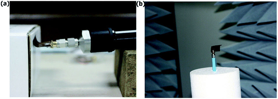
Reagent-grade ferric nitrate (Fe(NO3)3·9H2O), zinc nitrate (Zn2(NO3)·6H2O), and manganese nitrate (Mn2(NO3)·4H2O) were purchased from Sigma-Aldrich Company and used without any further purification; they were weighed according to the stoichiometric composition. The XRD patterns of the mixed ferrites were recorded with a Siemens D500 X-ray diffractometer using CuKα radiation and an angle range of 2θ: 20–60°. The structural morphology of the proposed substrate was observed by a Carl Zeiss Supra 55 VP SEM, operated at 15 kV. The optical property of the prepared ferrite substrates was measured from the absorption spectra using a double beam spectrometer from Perkin Elmer (Germany) Lambda-950 UV-Vis from 200 to 800 nm. A dielectric assessment kit (DAK 3.5) was employed to measure the dielectric properties within the frequency range of 1–6 GHz at room temperature. To measure the electromagnetic performances in bending conditions, all the fabricated substrates were bent 90° towards the radiating patch as shown in Fig. 1. The vector network analyzer (VNA) of PNA Series N5227A and Satimo hybrid StarLab in an anechoic chamber were deployed to measure the electromagnetic performances such as reflection coefficient, efficiency, gain and radiation patterns in a frequency range of 3–7 GHz, as shown in Fig. 1a and b.
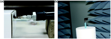 |
| | Fig. 1 Measurement setup for electromagnetic performances at bending condition, (a) VNA, (b) SATIMO. | |
Preparation of MnxZn(1−x)Fe2O substrate
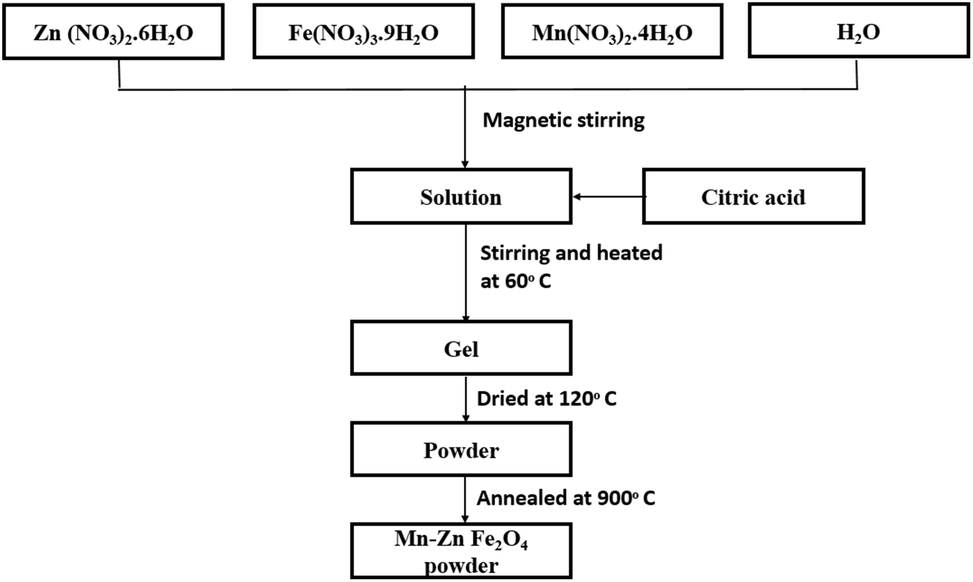
Zinc nitrate, manganese nitrate and ferrite nitrate were dissolved separately in distilled water to prepare mixed ferrite of several concentrations of Mn2+ (x = 0.0, 0.2, 0.4, 0.6 and 0.8) utilizing the sol–gel technique as shown in Fig. 2. Initially, zinc nitrate was dissolved in 75 mL of distilled water, followed by ferrite nitrate and manganese nitrate. The pH value of 6 was maintained with ammonia to produce the nanosized sample. For lower pH values, the Mn mixture may found to be incomplete; for higher pH values, there may be some loss of zinc. To complete the chemical reaction, the mixture was heated at 60 °C, continuously for around 5 h with constant magnetic stirring till the produced solution became sticky and transparent. To obtain the powder by evaporating the water completely, the sticky solution was dried in alumina crucible at 120 °C for 2 h. Afterwards, the grinding precursor was annealed at 900 °C for 1 h in the crucible furnace. Simultaneously, polyvinyl alcohol (PVA) was dissolved in distilled water to prepare the binder. Finally, the ferrite flexible substrate was obtained by mixing 1 g of the prepared ferrite powder and 10 mL of the PVA solution and dried at 70 °C for 7 h to completely evaporate the water. A 200 nm-thick silver/copper coating was sputtered on the ferrite substrate as a radiating patch and ground plane by magnetron sputtering.
 |
| | Fig. 2 Flowchart for sample preparation procedure for MnxZn(1−x)Fe2O4 compounds. | |
Results and discussion
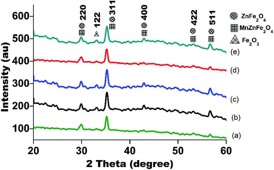
Fig. 3 shows the XRD patterns of the MnxZn(1−x)Fe2O4 substrates sintered at 900 °C. Three structural types of the crystalline phases of ZnFe2O4, MnZnFe2O4 and Fe2O3 were identified by indexing the patterns. The characteristic peaks of the ZnFe2O4, MnZnFe2O4 and Fe2O3 phases were found corresponding to the JCPDS files 01-0708731, 01-070-3821 and 01-058-0266, respectively. The added Mn2+ successfully emerged into the same phase in the samples, whilst being doped into the ZnFe2O4 lattice. The crystal structures of Mn/ZnFe2O4 peak resembles the standard face-centered-cubic structure (fcc)32 with a dominant peak (311). In Fig. 3, the major diffraction peaks are observed at 29.97°, 35.253°, 42.805°, 53.252° and 56.611° which represent (220), (311), (400), (422), (511) planes of ZnFe2O4 and MnZnFe2O4 structures, respectively. The XRD intensities of αFe2O3 (122) at 33.071° enhance gradually with increasing Mn2+ content. Moreover, the dominant peak shifts slightly towards a higher angle by increasing the concentration of Mn2+, which helps to improve the crystallizability by reducing the unit cell dimension.33–35
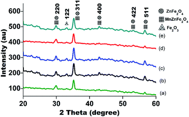 |
| | Fig. 3 XRD pattern of MnxZn(1−x)Fe2O4 for different concentrations (a) x = 0.0, (b) x = 0.2, (c) x = 0.4, (d) x = 0.6, (e) x = 0.8. | |
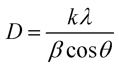
Generally, residual strain or stress increase the full width at half maximum (FWHM) of the peak because the residual stress and defects deform the lattice causing the peak to shift. Integration of Mn2+ and Zn2+ of different ionic radii also affects the shifting of the peak and the distortion.36 The lattice parameter tends to decrease with the shifting of the diffraction peak to a higher degree causing an increase in ceramic densities.37 The crystallite size D of the prominent peak (311) was calculated and listed in Table 1, using the Scherrer's equation formula:38
| |
 | (1) |
where,
k = 0.94, known as Scherrer constant,
λ is the X-ray wavelength (1. 54059 Å),
β is the broadening of the diffraction line measured at the half of its maximum intensity in radians and
θ is the angle of diffraction. The calculated crystallite size of ZnFe
2O
4 is 31.69 nm which is in good agreement with the reported results.
39 The crystallite size increases linearly from 31.69 nm to 38.21 nm with the increase of Mn
2+ concentration. Crystallinity increases with integration of Mn
2+ ions due to the incompatibilities between the ionic radii of Mn
2+ and Zn
2+ ions within the lattice host.
40 The crystallite size was affected by the variation of ionic radius between Mn
2+ (0.83 Å) and Zn
2+ (0.74 Å). On the basis of the XRD patterns, the lattice parameter (
a) of MnZnFe
2O
4 was measured from the following equation:
33| |
 | (2) |
where,
a is the lattice parameter (Å),
d is the interplanar distance (Å) and
hkl is the Miller index of the peaks (311). The experimental result reveals that the dominant peak shifted to the right (higher) angle upon the substitution of Zn
2+ with Mn
2+, which resulted in the decrease of lattice parameters from 8.443 Å to 8.420 Å. The evaluated lattice parameter of ZnFe
2O
4 are well agreed with the theoretical and reported value of 8.443 Å and
a = 8.444 Å,
39 respectively.
Fig. 4 shows the linear decrease in the lattice constant with Mn content follows the Vegard's law.
33 In material science and metallurgy, Vegard's law is the empirical heuristic that the lattice parameter of a solid solution of two constituents is approximately equal to a rule of mixtures of the two constituents' lattice parameters at the same temperature.
41
Table 1 Effect of composition on lattice constant and crystallite size for MnxZn(1−x)Fe2O4
| Composition x |
2θ (°) |
Lattice constant (Å) |
Crystallite size (nm) |
| 0.0 |
35.19 |
8.443 |
31.69 |
| 0.2 |
35.25 |
8.438 |
35.81 |
| 0.4 |
35.28 |
8.433 |
36.96 |
| 0.6 |
35.45 |
8.428 |
37.87 |
| 0.8 |
35.28 |
8.420 |
38.21 |
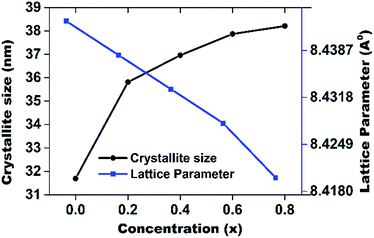 |
| | Fig. 4 Crystallite size and lattice parameter of MnxZn(1−x)Fe2O4 substrate with different concentration of Mn2+. | |
| | |
αA(1−x)Bx = (1 − x)αA + xαB
| (3) |
Vegard's law assumes that both components A and B in their pure form (i.e. before mixing) have the same crystal structure. Here, αA and αB are the lattice parameters of the pure constituents and x is the molar fraction of B in the solution.
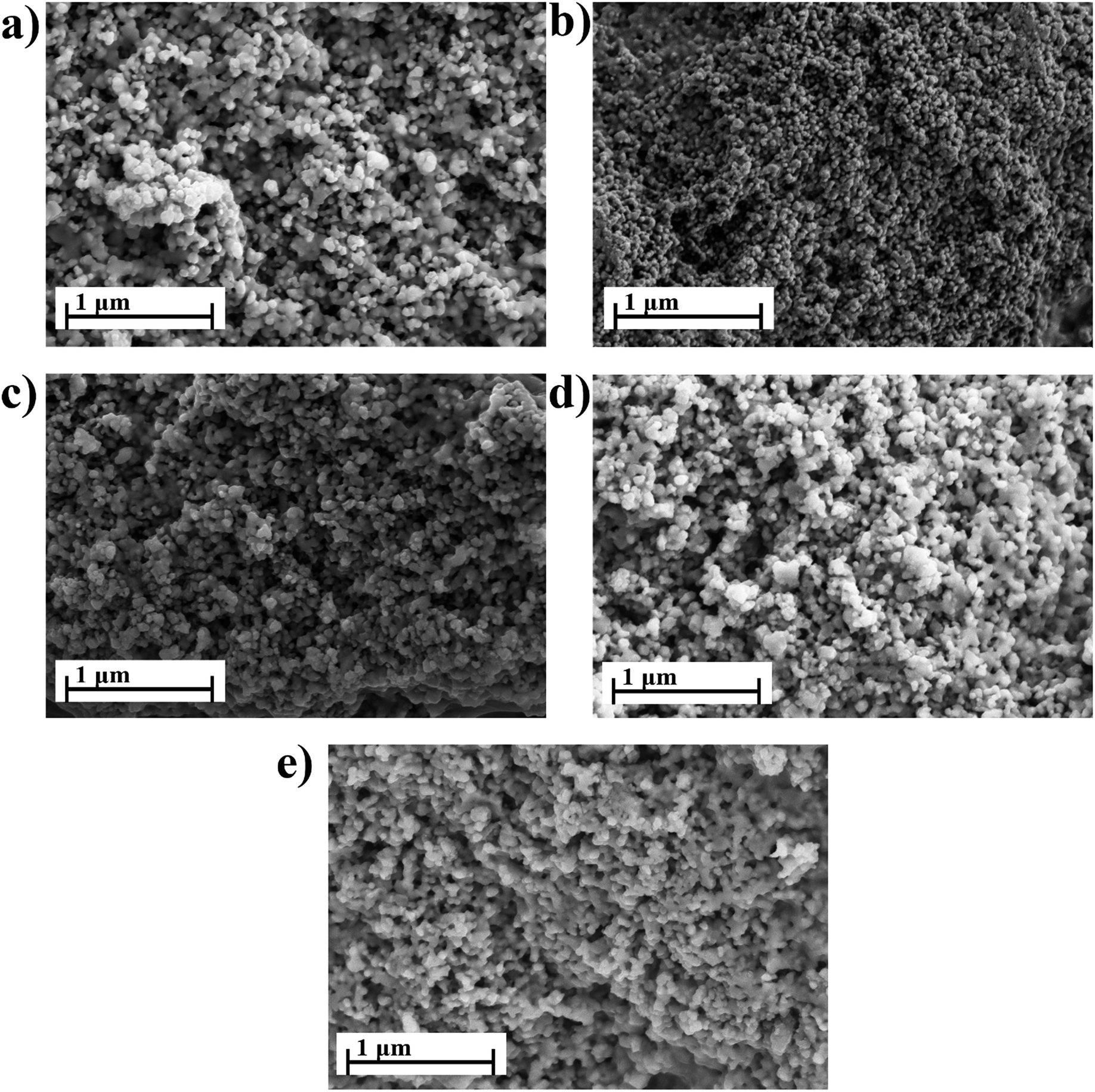
Fig. 5 shows the microstructure of (MnxZn(1−x)Fe2O4) samples sintered at 900 °C for 2 h with compositions of x = 0.0, 0.2, 0.4, 0.6 and 0.8. All samples appear to consist of some regular grains with a narrow distribution of grain sizes. The films have a spinel structure with cubic symmetry in the form of a regular octahedral. A magnetic interaction between the particles formed an agglomerated fine particulate in all samples. The average grain size of the mixed ferrite compounds varies with increasing Mn concentration: e.g., 66 nm (x = 0.0), 90 nm (x = 0.2), 92 nm (x = 0.4), 96 nm (x = 0.6) and 99 nm (x = 0.8). The dielectric loss decreases considerably with an increase in the average grain size. According to Chen,42 microwave dielectric loss is affected by many factors which consist of intrinsic and extrinsic losses. Moreover, intrinsic loss is associated with the vibration modes of the lattice and extrinsic loss is associated with the porosity, second phase, grain size, internal strain and lattice defects. An increase in the average grain size considerably improves the quality factor.
 |
| | Fig. 5 Scanning electron micrograph of MnxZn(1−x)Fe2O4 with x concentration (a) x = 0.0, (b) x = 0.2, (c) x = 0.4, (d) x = 0.6, (e) x = 0.8. | |
The absorption spectra of MnxZn(1−x)Fe2O4, in the transmission mode, were tested by dispersing the particles uniformly in liquid paraffin in the wavelength range of 200–800 nm. The intensity (I) of the transmitted beam through the sample was measured, then the absorption coefficient was calculated using eqn (3) with the preliminary measures of the intensity of the incident beam Io and the thickness of the sample d.38
| |
 | (4) |
The absorption coefficient of a direct bandgap semiconducting material can be evaluated from the following formula:38
| |
 | (5) |
where,
α is the absorption coefficient,
hν is the photon energy,
Eg is the bandgap and
A is a constant that depends on the type of transition.
Eqn (5) can be rearranged into the following form:
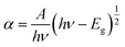
Hereafter, the optical band gap for the absorption peak was determined by extrapolating the linear portion of the plot shown in Fig. 6 to α = 0. The obtained value for ZnFe2O4 was 2.12 eV, which reveals the semiconductor behavior. As x increases, the optical bandgap decreases from 1.92 eV (x = 0.2) to 1.51 eV (x = 0.8), as shown in Fig. 6. In the literature, the bandgap for ZnFe2O4 ranges between 1.90 and 2.15 eV.42 However, not much information is available for the bandgap value of MnFe2O4 particles, except for a study performed by Guo et al. The bandgap values in this study are given as 1.68 and 1.74 eV for hollow spheres and a colloidal nanocrystal cluster respectively.43 The band-gap value is influenced by various factors such as film thickness, crystallite size, carrier concentrations, presence of impurities and deviation from stoichiometry of the film and lattice constant.44 The decrease in band-gap in the present case may be attributed to the decrease in lattice constant with Mn concentration. In addition, the band-gap decreases due to the increase in intermediary energy levels within the optical band gap. Wan Jalal et al. reported that decreasing the band gap can improve the dielectric properties, which is suitable for generating patch antennas.33
 |
| | Fig. 6 Variation of absorbance with wavelength of MnxZn(1−x)Fe2O4 powders, (a) x = 0.0, (b) x = 0.2, (c) x = 0.4, (d) x = 0.6, (e) x = 0.8. | |
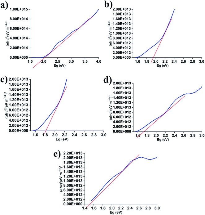
Cation distribution, grain size and synthesis techniques have an immense influence on the dielectric behavior of ferrite nanoparticles.45 The dielectric permittivity characteristic of the samples reveals that the permittivity value (ε′) varies with the applied frequency as shown in Fig. 7.
 |
| | Fig. 7 Variation of dielectric permittivity of MnxZn(1−x)Fe2O4 with applied frequency. | |
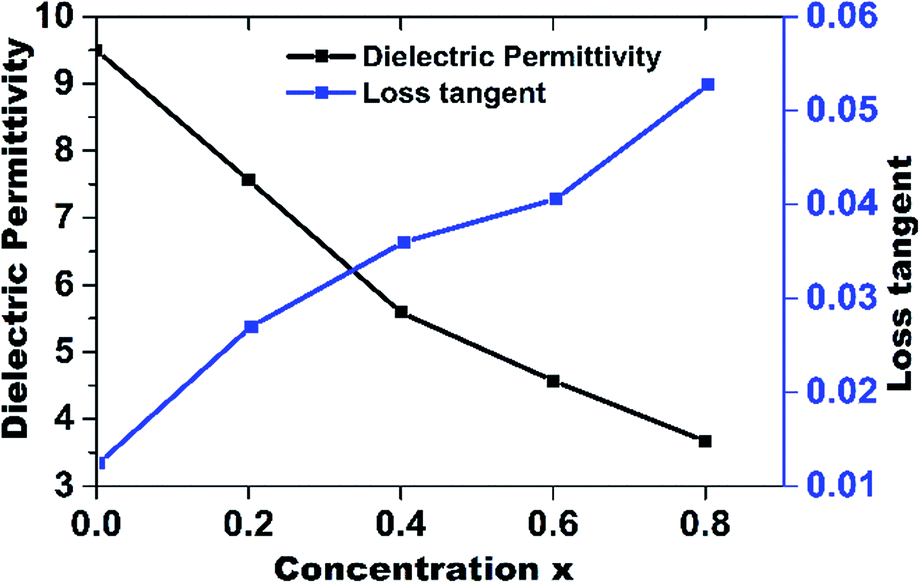
Characteristically, dielectric permittivity and dielectric loss fluctuate slightly with increasing frequency. Such a fluctuation can be characterized with the electron exchange interaction between Fe2+ and Fe3+, which cannot follow the external electric field.46 Other researchers reported similar behaviors for various ferrite systems.47,48 The dielectric constant for pure ZnFe2O4 is 9.52, whereas that for Mn-7.50 (x = 0.2), 5.56 (x = 0.4), 4.58 (x = 0.6) and 3.69 (x = 0.8). The decrease in εr caused by the increase in the number of pores as shown in SEM images in Fig. 5.
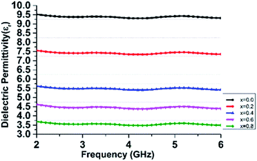
Fig. 8 shows the dielectric permittivity and loss tangent (tan![[thin space (1/6-em)]](https://www.rsc.org/images/entities/char_2009.gif) δ) of (MnxZn(1−x)Fe2O4) substrate with different degrees of Mn substitution within the frequency range of 1–6 GHz. There are two types of losses in dielectric materials. A conduction loss, due to the flow of electron charges and a dielectric loss caused by the atomic movement in an alternating field. Among the total core loss, dielectric loss plays an important role in microwave dielectric materials. The loss tangent is defined as the ratio of the loss in the reaction to the electric field E in the curl equation to the lossless reaction, which is less than 90°. The dielectric loss is measured from this loss tangent angle.
δ) of (MnxZn(1−x)Fe2O4) substrate with different degrees of Mn substitution within the frequency range of 1–6 GHz. There are two types of losses in dielectric materials. A conduction loss, due to the flow of electron charges and a dielectric loss caused by the atomic movement in an alternating field. Among the total core loss, dielectric loss plays an important role in microwave dielectric materials. The loss tangent is defined as the ratio of the loss in the reaction to the electric field E in the curl equation to the lossless reaction, which is less than 90°. The dielectric loss is measured from this loss tangent angle.
 |
| | Fig. 8 Dielectric permittivity and dielectric loss of MnxZn(1−x)Fe2O4 substrate with different concentration of Mn2+. | |
The dielectric loss for different compositions is tabulated in Table 2. The lowest dielectric loss of 0.012 was obtained for ZnFe2O4. The dielectric loss increased from 0.025 to 0.052 as x increased from 0.2 to 0.8.
Table 2 Impedance bandwidth and return loss characteristics along with dielectric permittivity and dielectric loss
| Concentration (x) |
Dielectric permittivity (εr) |
Dielectric loss (tanδ) |
Resonant frequency (GHz) |
Bandwidth (GHz) |
S11 (dB) |
| Bending |
Flat |
Bending |
Flat |
| 0.0 |
9.52 |
0.012 |
4.8 |
4.8 |
1.6 |
1.8 |
−19.6 |
| 0.2 |
7.50 |
0.025 |
4.4 |
4.4 |
1.3 |
1.3 |
−17.6 |
| 0.4 |
5.56 |
0.032 |
4.4 |
4.4 |
1.3 |
1.3 |
−14.8 |
| 0.6 |
4.58 |
0.040 |
4.4 |
4.8 |
1.3 |
1.6 |
−19.2 |
| 0.8 |
3.69 |
0.052 |
4.8 |
4.8 |
1.3 |
1.6 |
−18.0 |
Fabrication and electromagnetic performances
The dimension of the radiator plays an important role in the electromagnetic performances. The resonant frequency determined by the width (W) of the patch along with the material's dielectric permittivity (εr) according to the following equation:38| |
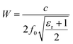 | (7) |
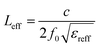
where, c denotes the speed of light in air and f0 refers to the resonant frequency. The effective permittivity (εreff) of the substrate is calculated using the following equation:38| |
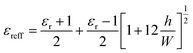 | (8) |
where h is the height of the substrate. Therefore, the effective patch length is calculated by using the value of the effective dielectric permittivity as follows:38| |
 | (9) |
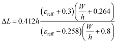
Considering the fringing field effect, the extended incremental length (ΔL) of the patch on both sides is measured as follows:38
| |
 | (10) |
Finally, the length of the patch is calculated from the following equation:38
The patch length of the radiator plays a critical role because of the inherently narrow bandwidth of the patch.
Fig. 9 shows the prototypes of the realized electromagnetic radiator. The proposed electromagnetic radiator fabricated on a flexible mixed ferrite substrate with a thickness of 1.2 mm. The electromagnetic radiator has a square patch with dimensions of 13 × 13 mm2, fed by a microstrip line. 50 Ω characteristics impedance was achieved with 3 × 6 mm2 microstrip feed line. A microstrip line with 3 mm width was connected to the radiation patch. On the back side of the substrate, a fractional ground plane of side length (Lg) 6 mm was fabricated. We utilized the magnetron sputtering for the copper coating of 200 nm thickness to fabricate the patch and ground plane of the electromagnetic radiator.
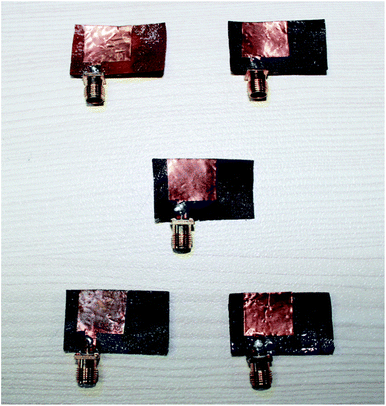 |
| | Fig. 9 Prototypes of the fabricated patch radiator. | |
The overall dimension of the radiating device is 29 × 19 mm2 and for experimental verification we prototyped the electromagnetic radiators. The simulation of the proposed electromagnetic radiator was performed using high frequency simulation software (HFSS) based on the finite element method. In this simulation, we applied the obtained dielectric permittivity and loss tangent value to measure the reflection coefficient. Fig. 10a–e show the measured (flat and bend) and simulated reflection coefficients against frequency for the proposed device. Measurements of all the electromagnetic radiators were performed between 3 to 7 GHz. The measured resonant frequencies were close to the simulation results. A small deviation was observed due to the fabrication tolerance. The measured results are tabulated in Table 2 along with the dielectric permittivity and dielectric loss.
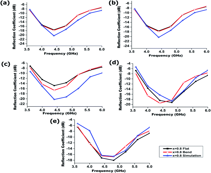 |
| | Fig. 10 Simulation and measured reflection coefficient of the electromagnetic radiator both at flat and bending conditions, (a) x = 0.0, (b) x = 0.2, (c) x = 0.4, (d) x = 0.6, (e) x = 0.8. | |
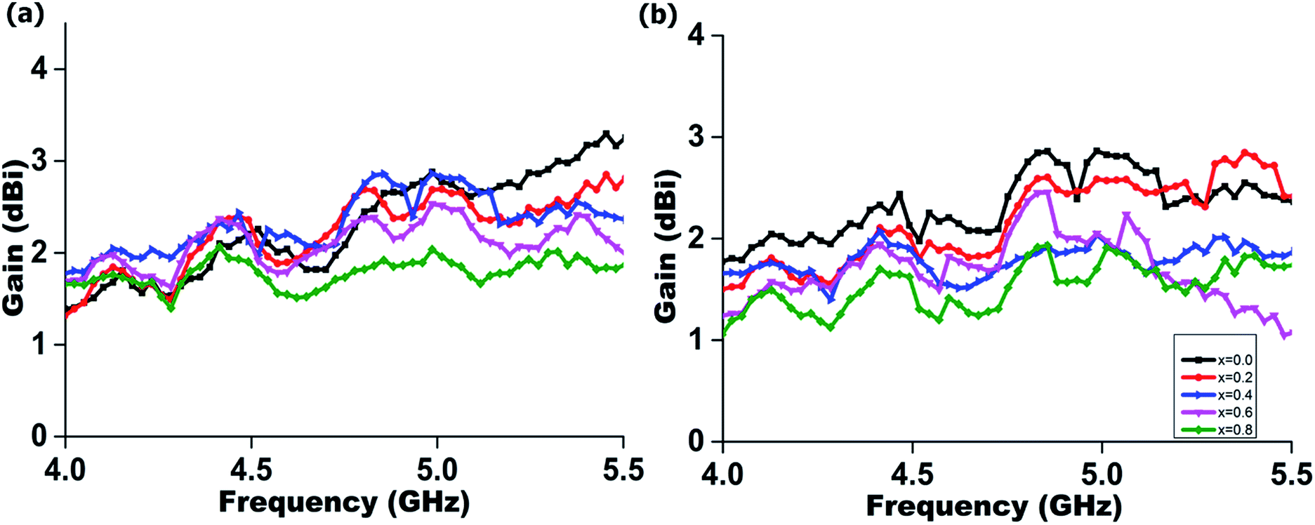
Fig. 11 illustrates the realized gain for both flat and bending conditions of the proposed radiator. Fig. 11 shows the measured realized gain of the proposed radiator at boresight (+z direction) in the operational frequency bandwidth. All the measured values are tabulated in Table 3. The electromagnetic radiators have a stable gain above 1.5 dBi throughout the operational frequency range. It is observed that the variations are less than 1 dBi between flat and bending conditions.
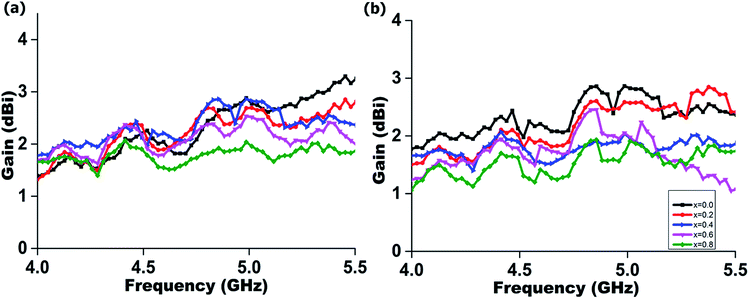 |
| | Fig. 11 Measured peak realized gain both at (a) flat and (b) bending conditions. | |
Table 3 Electromagnetic performances both at bending and flat conditions
| Composition (x) |
Efficiency (%) |
Gain (dBi) |
−3 dB (HPBW) (°) |
| Bending |
Flat |
Bending |
Flat |
Bending |
Flat |
| Max |
Avg |
Max |
Avg |
Max |
Avg |
Max |
Avg |
E-Plane |
H-Plane |
E-Plane |
H-Plane |
| 0.0 |
95 |
84 |
98 |
85 |
2.8 |
2.3 |
3.3 |
2.4 |
190 |
60 |
190 |
40 |
| 0.2 |
90 |
79 |
94 |
84 |
3.0 |
2.2 |
3.0 |
2.3 |
184 |
28 |
186 |
32 |
| 0.4 |
88 |
77 |
93 |
80 |
2.0 |
1.7 |
2.8 |
2.2 |
236 |
38 |
166 |
36 |
| 0.6 |
84 |
73 |
90 |
79 |
2.4 |
1.6 |
2.6 |
2.1 |
190 |
52 |
186 |
60 |
| 0.8 |
82 |
73 |
88 |
77 |
2.4 |
1.6 |
2.0 |
1.7 |
186 |
40 |
112 |
60 |
Fig. 12 depicts the measured radiation efficiency of the realized radiator at boresight. The average radiation efficiency is above 73% and 75% for bending and flat conditions respectively. All the measured data are tabulated in Table 3. It is obvious that the radiation efficiency of electromagnetic radiator will decrease with the increasing manganese concentration, as the dielectric loss increases simultaneously.
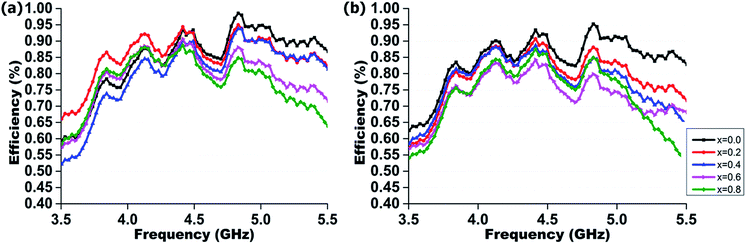 |
| | Fig. 12 Measured radiation efficiency both at (a) flat and (b) bending conditions. | |
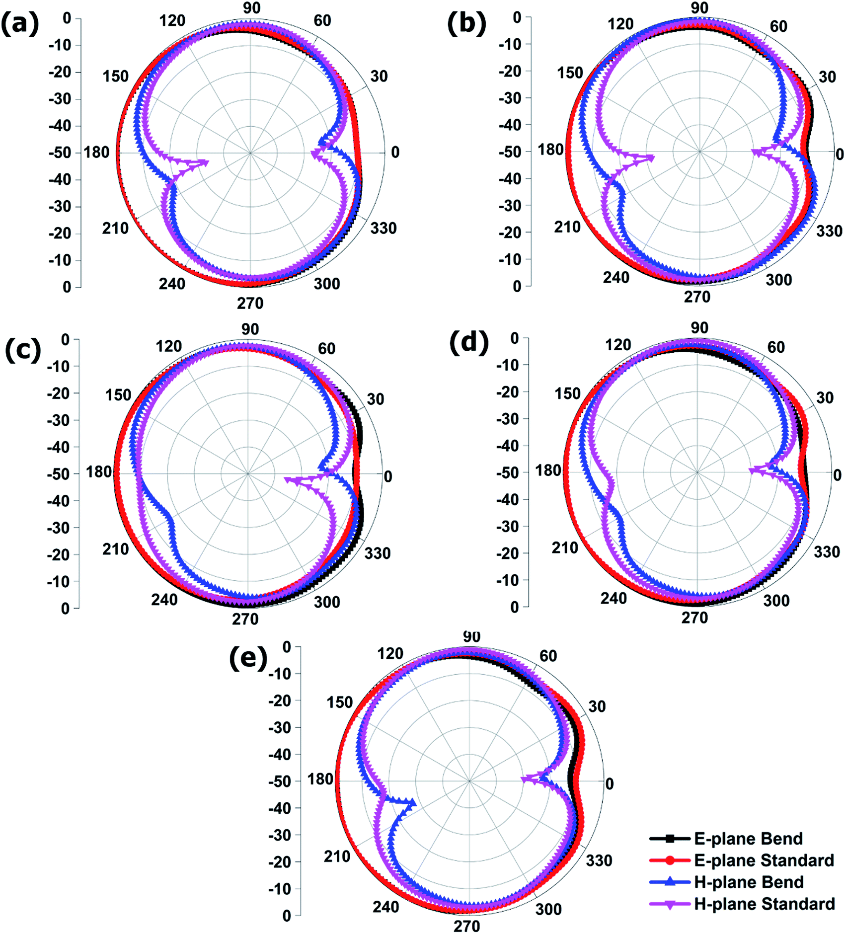
The measured radiation patterns, in both flat and bending conditions of the realized radiator are demonstrated in Fig. 13. An omnidirectional radiation pattern was observed for both cases, generated from the normalized E-plane. Moreover, a symmetric and stable radiation profile in both conditions was realized. A co-polar −3 dB half power beam width (HFBW) has been measured for all samples and tabulated in Table 3. From the table, it can be observed that there is no variation in the front lobe for both cases and a very negligible variation is observed in the back lobe. A considerable amount of back lobe was observed, which might be due to the utilization of the partial ground plane. A full ground plane can reduce this back lobe, which will cause low gain, low efficiency and narrow bandwidth. Fig. 13 also demonstrates the H-plane radiation pattern. It is found that, both the flat and bending radiators construct a donut-shape radiation pattern, resulting from nulls near 180° and 0° of the radiation pattern at the H-plane, which is consistent with the half wave dipole radiation pattern. A co-polar −3 dB half power beam width (HFBW) for the H-plane is also tabulated in Table 3.
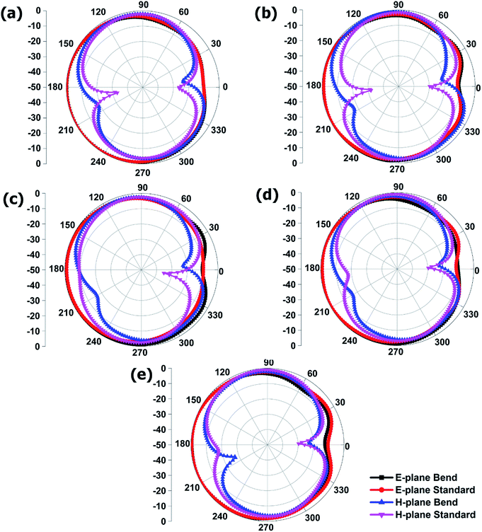 |
| | Fig. 13 Measured radiation pattern for flat and bending conditions, (a) x = 0.0, (b) x = 0.2, (c) x = 0.4, (d) x = 0.6, (e) x = 0.8. | |
Conclusions
This paper demonstrates the structural, morphological, dielectric characteristics and electromagnetic performances of the magneto dielectric flexible material. For the proof of concept, an electromagnetic radiator is fabricated on the proposed magneto dielectric substrate. The flexible substrate exhibits features such as high efficiency, adequate gain and stable radiation pattern without sacrificing the bandwidth at bending condition. A stable omnidirectional radiation pattern with a minimum average radiation efficiency above 73% and a minimum average realized gain beyond 1.5 dBi was achieved over the operating frequency range at bending condition. In conclusion, the optimal performances of the proposed flexible substrate validate its potential as a suitable candidate for flexible wireless communication and microwave imaging applications in the near future.
Acknowledgements
This work is supported by the University Research Grant (DIP-2015-014).
Notes and references
- R. A. Liyakath, A. Takshi and G. Mumcu, IEEE Antenn. Wireless Propag. Lett., 2013, 12, 603–606 CrossRef
 .
. - G. J. Hayes, J.-H. So, A. Qusba, M. D. Dickey and G. Lazzi, IEEE Trans. Antennas. Propag., 2012, 60, 2151–2156 CrossRef .
- Y. B. Pottathara, V. Bobnar, S. Gorgieva, Y. Grohens, S. Thomas and M. Finšgar, RSC Adv., 2016, 6, 49138 RSC .
- A. Rahman, M. T. Islam, M. Samsuzzaman, M. J. Singh and M. Akhtaruzzaman, Materials, 2016, 9, 358 CrossRef .
- J. Xi, H. Zhu and T. T. Ye, 2011 IEEE International Conference on RFID, 2011 Search PubMed .
- F. Axisa, D. Brosteaux, E. De Leersnyder, F. Bossuyt, M. Gonzalez, V. M. Bulcke and J. Vanfleteren, IEEE Polytronic 2007-6th International Conference on Polymers and Adhesives in Microelectronics and Photonics, 2007 Search PubMed .
- S. J. Chen, T. Kaufmann, R. Shepherd, B. Chivers, B. Weng, A. Vassallo, A. Minett and C. Fumeaux, IEEE Antenn. Wireless Propag. Lett., 2015, 14, 1207–1210 CrossRef .
- H. Bahramiabarghouei, E. Porter, A. Santorelli, B. Gosselin, M. Popovic and L. A. Rusch, IEEE Trans. Biomed. Eng., 2015, 62, 2516–2525 CrossRef PubMed .
- C. Williams, D. Chrisey, P. Lubitz, K. Grabowski and C. Cotell, J. Appl. Phys., 1994, 75, 1676–1680 CrossRef CAS .
- X. Huang, J. Zhang, W. Rao, T. Sang, B. Song and C. Wong, J. Alloys Compd., 2016, 662, 409–414 CrossRef CAS .
- X. Huang, J. Zhang, S. Xiao and G. Chen, J. Am. Ceram. Soc., 2014, 97, 1363–1366 CrossRef CAS .
- M. Jamalian, A. Ghasemi and E. Paimozd, J. Alloys Compd., 2014, 604, 373–378 CrossRef CAS .
- X. Huang, J. Zhang, W. Wang, T. Sang, B. Song, H. Zhu, W. Rao and C. Wong, J. Magn. Magn. Mater., 2016, 405, 36–41 CrossRef CAS .
- J. Shen, J. Feng, L. Li, G. Tong and Y. He, J. Alloys Compd., 2015, 632, 490–499 CrossRef CAS .
- X. Huang, J. Zhang, Z. Liu, T. Sang, B. Song, H. Zhu and C. Wong, J. Alloys Compd., 2015, 648, 1072–1075 CrossRef CAS .
- X. Huang, J. Zhang, M. Lai and T. Sang, J. Alloys Compd., 2015, 627, 367–373 CrossRef CAS .
- P. Gao, X. Hua, V. Degirmenci, D. Rooney, M. Khraisheh, R. Pollard, R. M. Bowman and E. V. Rebrov, J. Magn. Magn. Mater., 2013, 348, 44–50 CrossRef CAS .
- M. Atif, M. Idrees, M. Nadeem, M. Siddique and M. Ashraf, RSC Adv., 2016, 6, 20876–20885 RSC .
- C. H. Kwon, H.-K. Hong, D. H. Yun, K. Lee, S.-T. Kim, Y.-H. Roh and B.-H. Lee, Sens. Actuators, B, 1995, 25, 610–613 CrossRef CAS .
- G. Mangamma, V. Jayaraman, T. Gnanasekaran and G. Periaswami, Sens. Actuators, B, 1998, 53, 133–139 CrossRef CAS .
- L. Dan, P. Zhijian, C. Xuemin, W. Chengbiao, G. Huilin, F. Zhiqiang and Y. Yiyong, Rare Met. Mater. Eng., 2009, 38, 920–923 Search PubMed .
- A. Kool, P. Thakur, B. Bagchi, N. A. Hoque, S. Banerjee and S. Das, RSC Adv., 2015, 5, 104299–104313 RSC .
- L. Nalbandian, A. Delimitis, V. Zaspalis, E. Deliyanni, D. Bakoyannakis and E. Peleka, Microporous Mesoporous Mater., 2008, 114, 465–473 CrossRef CAS .
- M. Sertkol, Y. Köseoğlu, A. Baykal, H. Kavas and M. S. Toprak, J. Magn. Magn. Mater., 2010, 322, 866–871 CrossRef CAS .
- M. Barati, S. S. Ebrahimi and A. Badiei, J. Non-Cryst. Solids, 2008, 354, 5184–5185 CrossRef CAS .
- M. Gharagozlou, J. Alloys Compd., 2009, 486, 660–665 CrossRef CAS .
- S. Yáñez-Vilar, M. Sánchez-Andújar, C. Gómez-Aguirre, J. Mira, M. A. Señarís-Rodríguez and S. Castro-García, J. Solid State Chem., 2009, 182, 2685–2690 CrossRef .
- A. Xia and H. Zhang, Curr. Appl. Phys., 2010, 10, 825–827 CrossRef .
- C. J. Brinker and G. W. Scherer, Sol-gel science: the physics and chemistry of sol-gel processing, Academic press, 2013 Search PubMed .
- A. Katelnikovas, J. Barkauskas, F. Ivanauskas, A. Beganskiene and A. Kareiva, J. Sol-Gel Sci. Technol., 2007, 41, 193–201 CrossRef CAS .
- A. O. Karilainen, P. M. Ikonen, C. R. Simovski, S. A. Tretyakov, A. N. Lagarkov, S. A. Maklakov, K. N. Rozanov and S. N. Starostenko, IET microwaves, antennas & propagation, 2011, 5, 495–502 Search PubMed .
- A. Rahman, H. Abdullah, M. S. Zulfakar, M. J. Singh and M. T. Islam, J. Sol-Gel Sci. Technol., 2015, 1–10 Search PubMed .
- W. N. W. Jalal, H. Abdullah, M. S. Zulfakar, M. T. Islam, S. Shaari and B. Bais, J. Sol-Gel Sci. Technol., 2015, 74, 566–574 CrossRef CAS .
- J.-H. Park, S. Nahm and J.-G. Park, J. Alloys Compd., 2012, 537, 221–226 CrossRef CAS .
- W. Lei, W. Z. Lu, X. H. Wang, F. Liang and J. Wang, J. Am. Ceram. Soc., 2011, 94, 20–23 CrossRef CAS .
- W. Lei, W. Z. Lu, X. H. Wang, F. Liang and J. Wang, J. Am. Ceram. Soc., 2011, 94, 20–23 CrossRef CAS .
- J.-H. Park, S. Nahm and J.-G. Park, J. Alloys Compd., 2012, 537, 221–226 CrossRef CAS .
- A. Rahman, M. T. Islam, M. S. Zulfakar and H. Abdullah, J. Sol-Gel Sci. Technol., 2015, 74, 557–565 CrossRef CAS .
- S. Zhan, C. Gong, D. Chen and X. Jiao, J. Dispersion Sci. Technol., 2006, 27, 931–933 CrossRef CAS .
- H. Zhong, J. Wang, X. Chen, Z. Li, W. Xu and W. Lu, J. Appl. Phys., 2006, 99, 3905 Search PubMed .
- Y.-C. Chen, IEEE. Trans. Ultrason. Ferroelectrics. Freq. Contr., 2011, 58, 2531–2538 CrossRef PubMed .
- Y. Hou, X. Li, Q. Zhao and G. Chen, Appl. Catal., B, 2013, 142, 80–88 CrossRef .
- A. Baykal, S. Güner and A. Demir, J. Alloys Compd., 2015, 619, 5–11 CrossRef CAS .
- S. Chavan, M. Babrekar, S. More and K. Jadhav, J. Alloys Compd., 2010, 507, 21–25 CrossRef CAS .
- H. Abdelmoneim, Indian J. Pure Appl. Phys., 2010, 48, 562–570 CAS .
- G. R. Mohan, D. Ravinder, A. R. Reddy and B. Boyanov, Mater. Lett., 1999, 40, 39–45 CrossRef .
- V. Murthy and J. Sobhanadri, Phys. Status Solidi A, 1976, 36, K133–K135 CrossRef CAS .
- S. Mahalakshmi and K. S. Manja, J. Alloys Compd., 2008, 457, 522–525 CrossRef CAS .
|
| This journal is © The Royal Society of Chemistry 2016 |
Click here to see how this site uses Cookies. View our privacy policy here.