
Atomic layer deposition of ZnO/TiO2 multilayers: towards the understanding of Ti-doping in ZnO thin films
G. Torrisi*ab,
A. Di Maurob,
M. Scuderic,
G. Nicotrac and
G. Impellizzerib
aDipartimento di Fisica e Astronomia, Università degli Studi di Catania, via S. Sofia 64, 95123 Catania, Italy. E-mail: giacomo.torrisi.infn.it; giacomo.torrisi@ct.infn.it
bCNR-IMM, via S. Sofia 64, 95123 Catania, Italy
cCNR-IMM, Z.I. VIII Strada 5, Catania 95121, Italy
First published on 12th September 2016
Abstract
Undoped and Ti-doped ZnO (TZO) films were deposited by atomic layer deposition (ALD). Titanium was introduced by alternating consecutive ZnO cycles between each TiO2 single layer (Ti nominal concentration of 2%). The electrical, optical, morphological, and structural properties of the films (less than 80 nm thick) were tested as a function of the deposition temperature (from 120 to 240 °C). The TZO films deposited at 200 °C showed the lowest resistivity: 3.0 × 10⁻³ Ω cm. All the resulting TZO films were highly transparent, with an absorbance in the visible range of less than 3%. Thanks to an accurate investigation through transmission electron microscopy we ruled out the well-assessed explanation of an extrinsic doping mechanism of transparent conductive oxide (TCO), suggesting an alternative mechanism. These results demonstrate that the ALD is a promising technique to grow thin TZO films with remarkable electrical and optical properties.
1 Introduction
Transparent conductive oxide (TCO) films are frequently applied in many optoelectronic devices, such as photovoltaic cells, liquid crystal displays (LCDs), organic light-emitting diodes (OLEDs), and sensors.1,2 Indium tin oxide (ITO) films are mostly used due to their superior electrical transport properties.3 However, the toxicity, scarcity, and high price of In, pushes the replacement of ITO with other In-free compounds. To this aim, zinc oxide has been extensively investigated and employed as a transparent electrode owing to its excellent chemical and thermal stability, and specific electrical and optical properties.2,4 To increase the conductivity of ZnO, the addition of group-III elements, such as Al, Ga, In, and B, are commonly used.2 Recently, Ti-doped ZnO (TZO) films have been investigated for their promising electrical and optical properties.5–14 The literature is unanimous in explaining the extrinsic doping mechanism of titanium. Since Ti has valence 4+ but smaller ionic size than the host Zn 2+ cation, it is theoretically explained that when a Ti atom substitutes a Zn site in the ZnO crystal structure it provides two extra electrons contributing to the electrical conduction.9–11Several methods are used for the synthesis of TCO films: sputtering, roll-to-roll, printing, joule-effect evaporation, sol–gel, and chemical deposition.2,15,16 Recently, atomic layer deposition (ALD) has also attracted a significant interest as a promising method to deposit TCO films. ALD guarantees an excellent film uniformity, precise control of the thickness, high reproducibility, good crystalline quality, and it is easily scalable to industrial level.17–20 In addition, the concentration of doping in TCO films can be controlled by adjusting the ALD cycle ratio of the host material and the dopant one.21 Therefore, the ALD appears as the perfect technique to grow TCO and overcome the new technological challenges. It is worth noting that the TCO films synthesized by ALD have a layer-by-layer structure. For example, TZO films usually consist of a ZnO matrix and TiO2 dopant layers, rather than monodispersed Ti dopants, and this multilayer structure must be taken into account in explaining the electrical properties of the material (as reported for instance in ref. 22 for Al-doped ZnO deposited by ALD). However in the case of anion doping, a formation of layer-by-layer structure could be avoided by ALD through a mixing of dopant solution to an anion precursor solution (as reported for instant in ref. 23 for F-doped ZnO deposition by ALD).
The literature reports only few papers focused on TZO films grown by ALD. Ye et al., Bergum et al., and Wan et al., reported the effect of various Ti doping concentration on the structural, electrical, and optical properties of TZO films deposited at 200 °C.9–11
In this work, we studied the electrical, optical, and structural properties of TZO films grown by ALD at different deposition temperatures (from 120 to 240 °C), fixing the Ti nominal concentration (2%) and the film thickness (100 nm). The extrinsic doping mechanism has been investigated and a simple model will be proposed.
2 Experimentals
ZnO and TZO films were deposited thermally by ALD, employing the R-200 Advanced reactor by Picosun. Two substrates were used: quartz (for electrical and optical characterizations), and silicon (for morphological and structural analyses). Diethyl zinc (DEZ, purity ≥ 99.9999%), and de-ionized water were used as precursors for the deposition of ZnO, while TiCl4 (purity ≥ 99.995%) and de-ionized water were used as precursors for TiO2. N2 was used as carrier and purge gas (purity ≥ 99.999%). The pulse and the purge times were kept constant at 0.1/3/0.1/5 s for DEZ/N2/H2O/N2, and 0.1/8/0.1/5 s for TiCl4/N2/H2O/N2. The Ti content in the TZO films was nominally fixed at 2% by controlling the number of DEZ and TiCl4 cycles. The film thickness was nominally fixed at 100 nm. During the depositions the temperature was settled at 120, 160, 200, or 240 °C.The film thickness, along with the refractive index, were evaluated by the Woollam M-2000 spectroscopic ellipsometer, using a Cauchy model in the 400–1700 nm range. The uniformity of the films resulted lower than 2% on 8′′ silicon wafers.
The composition of the multilayers, and in particular the atomic percentage of Ti, were investigated by Rutherford backscattering spectrometry (RBS), with a 3.5 MeV HVEE Singletron accelerator, using a 2.0 MeV He+ beam with 165° scattering angle.
The electrical characterization was carried out by means of four-point probe and Hall effect measurements, at room temperature, by using the BioRad HL5560 equipment. The applied magnetic field was 0.322 T. The samples, patterned according to van der Pauw geometry, were square-shaped (1 cm × 1 cm) and contacted by four Au sputtered contacts. This technique allows the determination of the sheet resistance, Hall carrier dose and mobility (the latter determined by the first two quantities). The sheet resistance and the carrier Hall dose are affected by a maximum error of ∼5%.
The optical characterization was obtained by extracting both the normal transmittance (T) and the 20° reflectance (R) spectra in the 300–1500 nm wavelength range, by using the Varian Cary 500 double beam scanning UV/VIS/NIR spectrophotometer.
The surface sample morphology was investigated by field emission scanning electron microscopy (SEM), using the Zeiss Supra 25 microscope operating at 3.0 kV.
The crystallinity of the films was investigated by X-ray diffraction (XRD) analyses with the Bruker D-500 diffractometer (detector scan mode) at 0.8° angle of incidence, and 2θ from 20° to 60°. The XRD spectra were analyzed by the Bruker software suite, including ICSD structure database.
Structural characterization was performed on a cross-sectional view of the TZO films through transmission electron microscopy (TEM). The probe Cs corrected JEOL JEM ARM200CF microscope was used at a primary beam energy of 200 keV, operated in both conventional TEM (C/TEM) and in scanning TEM mode (S/TEM). This particular configuration is equipped with a fully loaded post column GIF Quantum ER as electron energy loss spectrometer (EELS). Fine structure analysis of the EELS spectra, also called electron energy loss near-edge structure (ELNES), was used to investigate whether TixOy oxidation states different that the deposited TiO2 have been formed.
3 Results and discussion
3.1 Film growth
Different TZO films were prepared by ALD, by changing the deposition temperature from 120 up to 240 °C. Multiple ZnO ALD cycles and one TiO2 ALD cycle were repeated many times, as schematically depicted in Fig. 1. One “supercycle” of TZO was defined as m cycles of ZnO plus one subsequent cycle of TiO2. The total number of supercycles will be hereafter indicated with M. The nominal titanium fraction (% TiNom) is defined in literature as the fraction of Zn atoms replaced with Ti (i.e., Ti/(Ti + ZnO)). Once fixed the nominal Ti concentration at 2% (that appears promising from literature),17,18 the m cycles of ZnO were calculated through the following relation:21
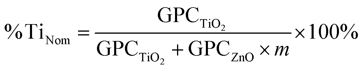 | (1) |
| Thickness = M × (GPCZnO × m + GPCTiO2) | (2) |
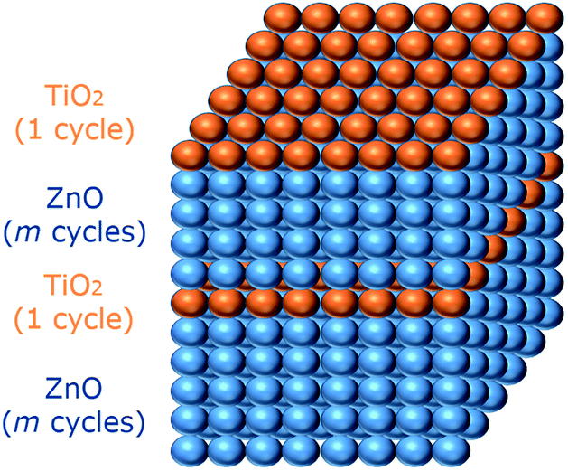 | ||
| Fig. 1 Scheme of the deposition process: m cycles of ZnO and one TiO2 cycle, repeated M times. | ||
These parameters (i.e. m, M, the measured thickness, and the nominal Ti percentage % TiNom) are listed in Table 1 for the four TZO samples deposited at the different temperatures: 120, 160, 200, and 240 °C. Undoped ZnO films with the same TZO thickness (the measured one) and deposition temperature were grown as references.
| Temperature (°C) | m | M | Thickness (nm) | % TiNom | % TiRBS |
|---|---|---|---|---|---|
| 120 | 15 | 33 | 82.0 | 2 | 3 |
| 160 | 13 | 38 | 68.5 | 2 | 3.5 |
| 200 | 14 | 44 | 68.1 | 2 | 4 |
| 240 | 14 | 50 | 53.6 | 2 | 7 |
The first analysis concerned the film growth behaviour. The GPC for pure ZnO and TiO2 was obtained by depositing ZnO and TiO2 for 100, 200, or 300 cycles, for each investigated temperatures.
Fig. 2 reports the film thickness as a function of the number of the ALD cycles for ZnO (circles) and TiO2 (triangles) deposited at 120 (a), 160 (b), 200 (c), and 240 °C (d).
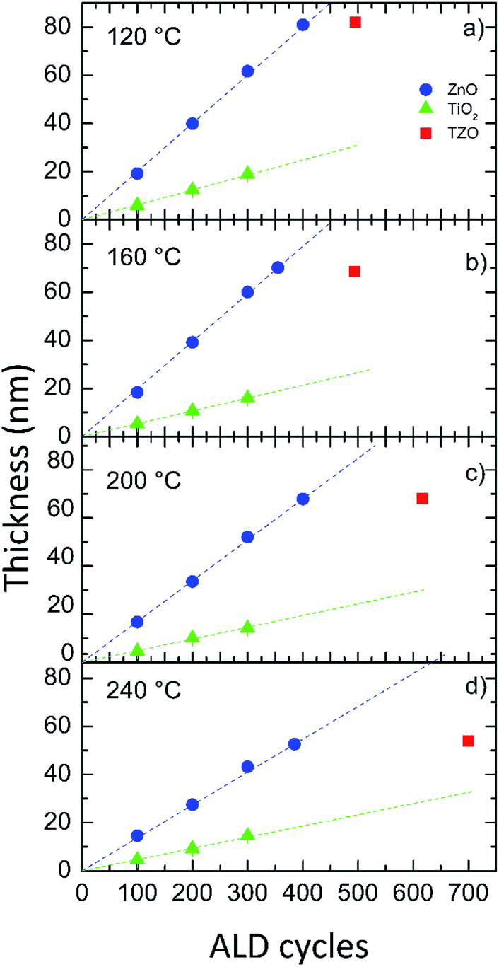 | ||
| Fig. 2 Film thickness of ZnO (circles), TiO2 (triangles), and TZO (squares) films as a function of the number of ALD cycles deposited at 120 (a), 160 (b), 200 (c), and 240 (d) °C. | ||
The error in the evaluation of the thickness, within the 2%, was the standard deviation deduced by the ellipsometrical measurements (317 measurements on each 8′′ silicon wafer) and it is within the symbol sizes. The trends of the film thicknesses were linear with respect to the number of the ALD cycles, indicating a self-limiting growth of the films. The linear fits of the experimental data (reported in Fig. 2 as dashed lines) give the growth rates reported in Table 2. Fig. 3 reports the GPC of ZnO (a) and TiO2 (b) films as a function of the different deposition temperatures. The growth rate for ZnO are relatively higher than the ones reported in literature, but with a similar trend.24 In detail, the ALD growth window for ZnO was estimated to range from 100 to 170 °C,24 in good agreement with the results of this work (see Fig. 3(a)). The growth rate for TiO2 reported in Fig. 3(b) decreases from 120 to 200 °C, and remains constant from 200 to 240 °C. Both the GPC values and the trend are consistent for what reported for TiO2 deposition24 (see also ref. 26 and 27, for the case of tetrakis-dimethyl-amido titanium precursor). The ALD growth window for TiO2 was found to be in the temperature range from 200 to 400 °C,25 in agreement with our data (see Fig. 3(b)). The GPC of TZO films (squares in Fig. 2) always resulted lower than the expected one. The measured thicknesses reported in Table 1 are always off-target (100 nm nominally). This decrease is consistent with a reduced adsorption of DEZ on TiO2, indicating a surface-hindered growth, in good agreement with what reported in literaure.9,10
| Sample | Temperature (°C) | GPC (nm) |
|---|---|---|
| ZnO | 120 | 0.200 |
| TiO2 | 120 | 0.062 |
| ZnO | 160 | 0.193 |
| TiO2 | 160 | 0.053 |
| ZnO | 200 | 0.170 |
| TiO2 | 200 | 0.048 |
| ZnO | 240 | 0.140 |
| TiO2 | 240 | 0.049 |
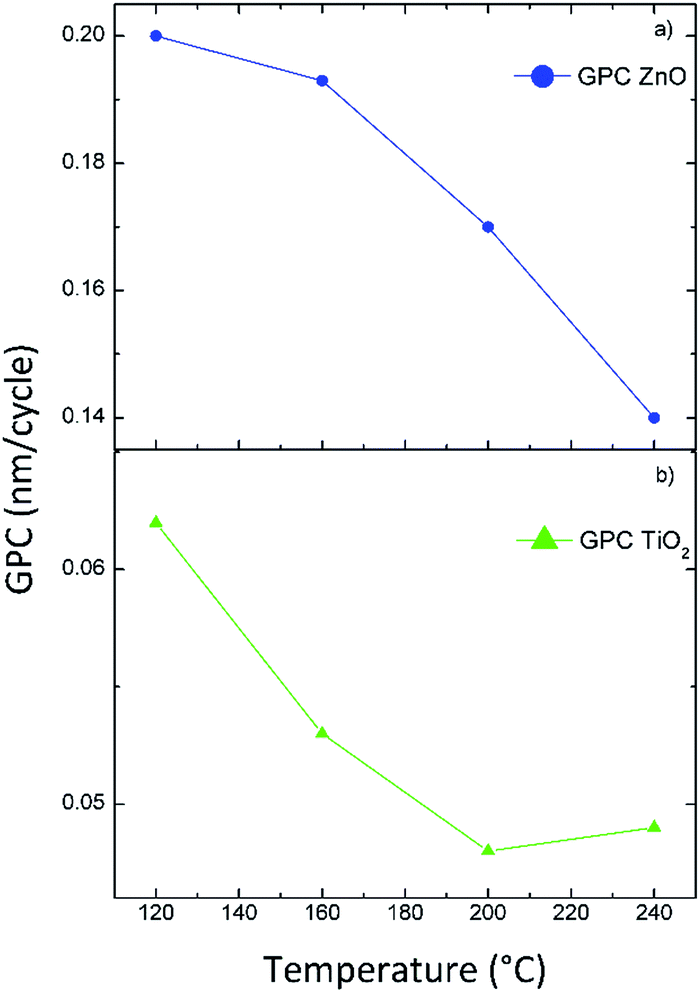 | ||
| Fig. 3 Growth rate per cycle as a function of the deposition temperature for ZnO (a) and TiO2 (b) films. | ||
In order to evaluated the atomic percentages of Ti inside the multilayers, we used RBS analysis. Fig. 4 reports (with diamonds) the RBS spectrum of the TZO films deposited at 200 °C. The continuous line indicates the simulation of the spectrum obtained by the XRUMP code.28 The multilayer composition resulted to be: Zn at 44%, O at 52% and Ti at 4%.
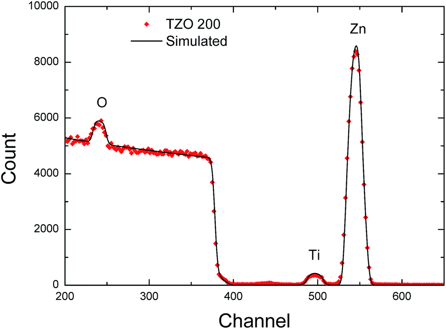 | ||
| Fig. 4 RBS spectra of TZO film at 200 °C. | ||
The real Ti concentration (4%) was found to deviate from the nominal one (2%), as expected by the deviation of the multilayers thicknesses discussed before. The atomic percentages of Ti in the different synthesized materials are reported in Table 1, last column (% TiRBS).
3.2 Electrical properties
In order to evaluate the performance of the TZO films as electrodes, the electrical properties were investigated by combining four-point probe and Hall effect measurements. Fig. 5 reports the resistivity (a), the Hall carrier concentration (b) and the Hall mobility (c), as a function of the deposition temperature for TZO (squares) and ZnO (circles) films. In particular, the resistivity values were obtained by the sheet resistance (measured by the four-point probe) times the layer thickness. The carrier concentration was estimated by dividing the Hall carrier dose (quantified by the Hall effect measurements) by the layer thickness.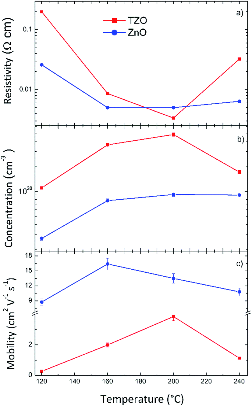 | ||
| Fig. 5 Resistivity (a), Hall carrier concentration (b), and mobility (c) as a function of the deposition temperature for TZO (squares), and ZnO (circles) films. | ||
Plotting the Hall carrier dose would be more rigorous, since we image the carriers not uniformly distributed along the thickness of the layers. Nevertheless, the carrier concentration allows an easy comparison with the existing literature. The mobility values were obtained from four-point probe and Hall effect measurements.
The sign of the Hall voltage revealed the presence of n-type carriers both in ZnO and TZO materials, as expected.
The carrier concentration are always higher in the TZO films, with respect to the ZnO films (up to a factor of ∼5), indicating a doping of the material thanks to the presence of titanium (see Fig. 5(b)). The temperature seems to favour the carriers up to 200 °C. The carrier concentration reaches a maximum of ∼5 × 1020 cm−3 in the TZO films deposited at 200 °C. On the other hand, the mobility is negatively influenced by the titanium, indeed the mobility values are always lower in TZO materials than in ZnO (see Fig. 5(c)). The temperature promotes the carrier mobility up to 200 °C in the TZO. The best value for TZO was obtained at 200 °C (∼4 cm2 V−1 s−1). As a result of the carrier concentration and mobility values, the resistivity reaches a minimum value at 200 °C in TZO: ∼3 × 10⁻³ Ω cm. Considering the real Ti concentration of 4%, the results obtained at 200 °C are roughly in agreement to what reported in literature for titanium tetraisopropoxide.9,10 Our results clearly show that temperatures below and above 200 °C do not improve the electrical performance of the TZO.
3.3 Optical properties
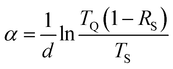
The optical transparency of the TZO films was investigated by UV/VIS/NIR spectroscopy.Fig. 6(a) reports on the left vertical axis the transmittance for TZO film (continuous line) and its reference ZnO film (dashed line) deposited at 200 °C. The TZO film showed a high transmittance (>76%) in the entire visible range (from 400 to 800 nm). On the vertical right axis of Fig. 6(a) the reflectance for TZO film (continuous line) and its reference ZnO film (dashed line) deposited at 200 °C are reported. Similar results were obtained for other investigated deposition temperatures (not shown). Fig. 6(b) shows the absorbance for TZO film (continuous line) and its reference ZnO film (dashed line) deposited at 200 °C. The absorbance (A) was obtained by the transmittance (T) and reflectance (R) measured spectra, in accordance with the following equation: A% = 100% − T% − R%. Both films have a very low absorbance in the visible range, below about 3% in the 400–800 nm range. Instead, in the UV part of the spectrum the films show the typical optical absorption, due to their band-gap energy.
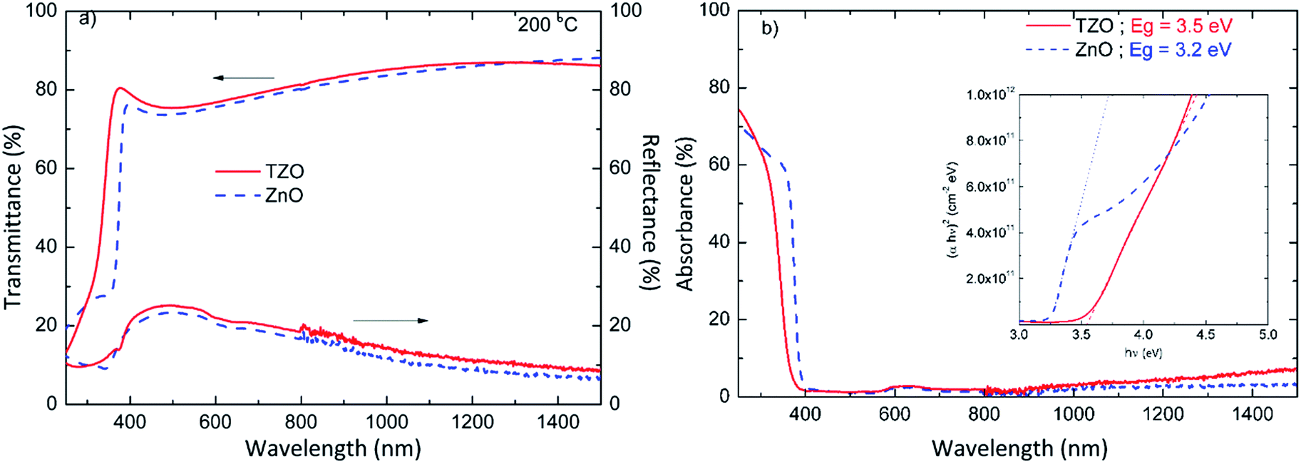 | ||
| Fig. 6 (a) Transmittance and reflectance spectra for TZO (continuous line) and ZnO (dashed line) films deposited at 200 °C. (b) Absorbance spectra for TZO (continuous line) and ZnO (dashed line) films deposited at 200 °C. The inset reports the Tauc plot together with the linear fits (dotted lines). | ||
The optical band-gap of the films can be calculated according to the Tauc model, which describes the light absorption process in amorphous semiconductors.29 The pertinence of the model was demonstrated also for polycrystalline semiconductors, and in particular for ZnO.30 According to this model the optical absorption strength depends on the difference between the photon energy and the band-gap energy as follows:
| (αhv)1/n = B(hv − Eg) | (3) |
 | (4) |
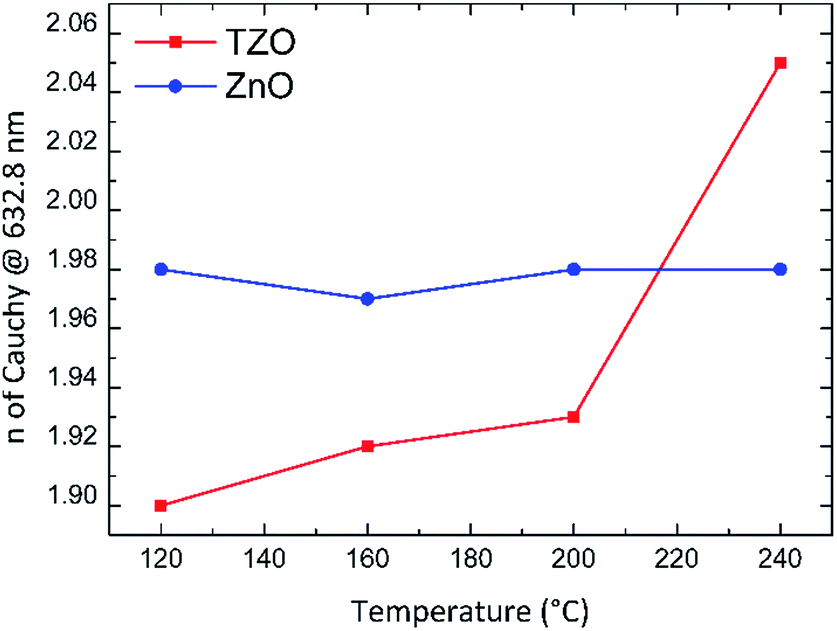 | ||
| Fig. 7 Index of refraction at 632.8 nm as a function of the deposition temperature for TZO (squares) and ZnO (circles) films. | ||
3.4 Morphological and structural properties
The morphological and structural investigations of TZO and ZnO are presented in this section. Fig. 8 shows top-view SEM images of pure ZnO ((a) for the deposition temperature of 120 °C, (c) for 160 °C, (e) for 200 °C, (g) for 240 °C) and TZO ((b) for the deposition temperature of 120 °C, (d) for 160 °C, (f) for 200 °C, (h) for 240 °C). The ZnO and TZO deposition provided surfaces with uniform elongated grains. From a comparison between the SEM images of the two materials the grain sizes are smaller in the TZO films.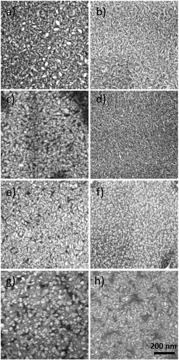 | ||
| Fig. 8 Plan-view SEM images of ZnO deposited at 120 °C (a), 160 °C (c), 200 °C (e), 240 °C (g), and TZO deposited at 120 °C (b), 160 °C (d), 200 °C (f), 240 °C (h). | ||
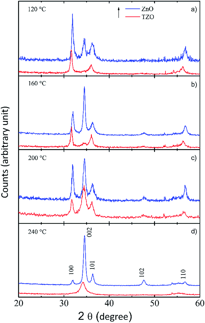
In Fig. 9 the XRD peaks of the TZO and ZnO deposited at different temperatures are reported ((a) for 120 °C, (b) for 160 °C, (c) for 200 °C, (d) for 240 °C). XRD analysis revealed that both ZnO and TZO thin films were polycrystalline with a hexagonal wurtzite structure. The diffraction of the ZnO thin films show well-defined Bragg peaks corresponding to the planes (100), (002), (101), (102) and (110). The crystal orientation of the films strongly depends on the deposition temperature. At 120 °C the (100) contribution is dominant indicating that the ZnO grains are mainly oriented along the c-axes parallel to the layer surface.34 Upon increasing the deposition temperature, from 160 to 240 °C, the (002) reflection gradually gets more intense, indicating that in this temperature range the ZnO prefers to grow with the c-axis perpendicular to the layer surface. The diffraction patterns of TZO films are quite similar to those of the ZnO thin films, but with some differences. In more detail, the peak at 34.5°, related to the (002) reflection, is missing in the TZO sample grown at 120 °C, while appears and increases in intensity with the deposition temperature. The TZO film deposited at 200 °C shows the most pronounced (002) reflection, that can be correlated to the best electrical properties observed for this sample (see Fig. 5).
 | ||
| Fig. 9 XRD spectra of TZO and ZnO films deposited at 120 °C (a), 160 °C (b), 200 °C (c), 240 °C (d). | ||
Moreover, no peaks associated to the presence of Ti or TiO2 are observed in the XRD plots. Fig. 9 also shows a shift in the TZO peaks with respect to the ZnO ones towards lower diffraction angles. This shift in the peak position can be correlated to a tensile strain induced by the presence of the TiO2 into the ZnO matrix.
Cross-sectional TEM views of the TZO film with the best electrical performance, i.e. the one deposited at 200 °C, are reported in Fig. 10. A low magnification bright field image (Fig. 10(a)) shows, from the bottom to the top, the Si substrate, the TZO film, the epoxy glue used for cross-section TEM sample preparative. The thickness of the TZO film was estimated to be ∼66 nm, in very good agreement with the ellipsometric measurements (∼68 nm, as reported in Table 1). The corresponding dark field image (Fig. 10(b)) shows a polycrystalline film with columnar grains. The presence of crystal domains extending vertically for the entire crystal thickness shows that TiO2 ALD cycles do not interrupt the growth of the ZnO grains.
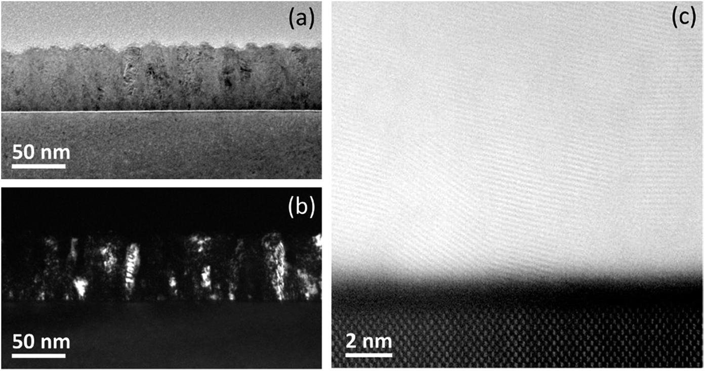 | ||
| Fig. 10 (a) Cross-sectional bright field image of TZO film deposited at 200 °C, and (b) the corresponding dark field image. (c) High resolution Z-contrast STEM image of the TZO film. | ||
The diffraction analysis (not shown) unequivocally showed a polycrystalline wurtzite phase of the TZO, in perfect agreement with the XRD spectra (see Fig. 9).
The atomic resolution Z-contrast S/TEM image reported in Fig. 10(c) shows the mono-crystalline structure of the Si substrate where the two silicon atoms of the dumbbell structure along the direction 〈110〉 are visible (on the bottom). The presence of a ∼2 nm thick amorphous native SiO2 layer on the Si surface is clearly evidenced, pointed out by the dark uniform contrast. While, on top of it the polycrystalline nature of the TZO film is revealed. In particular, the absence of any interruption into the columnar grains suggests that the TiO2 does not inhibit or influence the ZnO grain growth, as one might expect if a layer-by-layer growth should occur.
Electron energy loss spectroscopy (EELS) spectrum imaging (SI) techniques,35,36 performed at the Si/TZO interface, allowed the Ti chemical mapping. In particular, Fig. 11 shows an elemental map of Ti (edge L3,2) putting in evidence the presence of Ti nanodots with a mean diameter of ∼2 nm. The SI techniques is a complementary technique to the energy filtered TEM (EFTEM) and could be used in STEM mode, allowing the direct identification of the chemical species with much more high spatial resolution.37
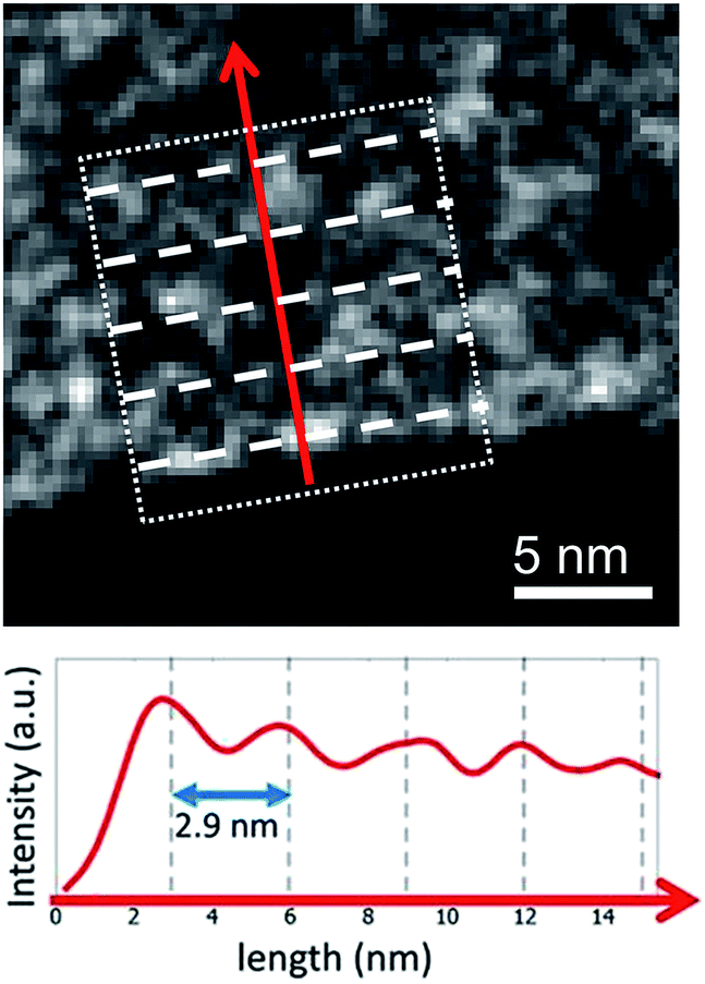 | ||
| Fig. 11 Elemental EELS map of Ti (edge L2,3) showing Ti nanodots with a mean diameter of ∼2 nm. At the bottom, an intensity linescan on the region indicated on the map puts in evidence the periodicity of Ti signal along the film thickness. | ||
The chemical map is obtained by selecting the corresponding ionization edge from the EELS spectrum, acquired pixel by pixel on the scanned area, by the small beam electron probe. The map shows a brighter signal in correspondence of the Ti atomic edge. An intensity linescan, acquired on the Ti maps, and plotted on the bottom of Fig. 11, shows that the Ti concentration along the thickness of the film follows the sequence of ZnO and TiO2 during the growth (∼3 nm). In detail, the peak-to-peak distance (2.9 nm) approximately corresponds to the ZnO thickness between the TiO2 layers (∼2.4 nm), estimated from the film growth rate.
In order to understand how the TiO2 chemically reacted with the ZnO matrix, ELNES spectrum analysis of Ti L3,2 and O K edges, integrated into the whole ZnO layer, were acquired and reported in black in Fig. 12. We removed the background signal and plural scattering contribution by using the Fourier-ratio technique. This is possible thanks the simultaneous presence of the zero loss peak, held possible in our particular configuration system, which also assure the precise control of the peak positions by excluding trivial energy drift of the spectrometer. The interpretation of ELNES fine structure in not always straightforward, since the intensity and feature positions effectively reflects the unfilled density of states (DOS) above the Fermi energy level, which in turn are extremely sensitive to changes in the bonding or the valence state of the atom. But in many case a fingerprinting approach may help on the understanding of the system under investigation.38 For this reason the acquired spectrum were compared with the ones of five different oxides reported in literature. In particular, the cubic TiO, Ti2O3, anatase and rutile TiO2 are depicted in Fig. 12, as reported by Stoyanov et al.39 The amorphous TiO2 is also reported in Fig. 12, as found by Bertoni et al.40 By the comparison of the different spectra we can argue that our experimental spectrum has the L3 and L2 edges, also called white lines, on the same energy position of TiO2 anatase and amorphous TiO2, at 460 and 466.25 eV, respectively. But only the anatase has two secondary peaks before the white lines, at around 458 and 463 eV, respectively. Moreover, our experimental spectrum shows the same shoulder on the right hand side of the L3 feature at 460.7 eV, present only on the anatase mineral form. It was experimentally reported that Ti oxides reveal that the L3,2 onset shifts of about 1.7–2.0 eV to lower energy with decreasing the oxidation state.39 The change of the intensity ratio between the two white lines and the pre-edge peak could be explained in terms of crystal field distorsion, and the sub splitting of the L2 prepeak.42 We can than surely exclude the presence of other polymorphism of TixOy and in particular of the TiO form, since it has the two white lines too far away, at 457.4 and 462.5 eV, a distance well above our energy resolution of 0.4 eV.
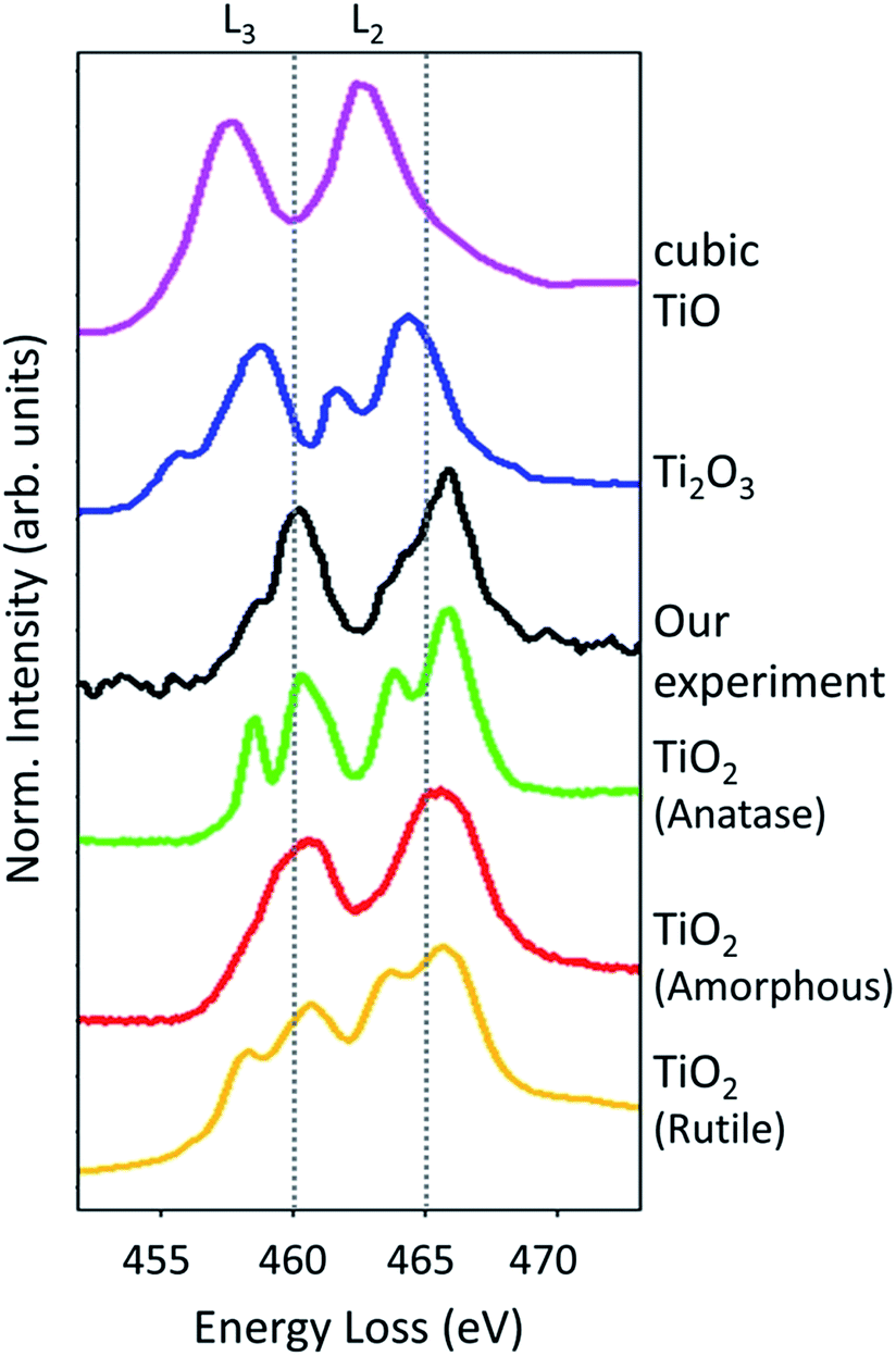 | ||
| Fig. 12 Ti L3,2 ELNES spectra of our analyzed Ti oxide, and 5 different oxides reported in literature by comparison, stacked with the valence state of Ti decreasing from the bottom to the top. | ||
4 Discussion
ZnO, a n-type semiconductor, is included in TCO for its light transmittance and electrical conductivity properties.2,4 The conductivity of intrinsic ZnO, i.e. without intentional addition of dopants, is ascribable to intrinsic donor dopants, such as oxygen vacancies or zinc atoms on interstitial lattice sites.2 The ALD grown materials (from 120 to 240 °C) reported in this paper allowed to obtain polycrystalline ZnO films (see Fig. 9), with high transmittance (>76%) in the visible range (see dashed line in Fig. 6(a)), with a carrier concentration ∼ 8 ÷ 9 × 1014 cm−3 (from 160 °C), a mobility of ∼16 ÷ 11 cm2 V−1 s−1, and a resistivity down to ∼5 × 10⁻³ Ω cm (see Fig. 5).Since undoped ZnO films have relatively low carrier concentration (see circles in Fig. 5(b)), extrinsic doping with Ti were adopted to improve the conductivity. The titanium was introduced during the ALD process by alternating one TiO2 cycle in between multiple ZnO cycles. This extrinsic doping allowed to obtain polycrystalline TZO films (see Fig. 9 and 10) with high transmittance (>76%) in the visible range (see continuous line in Fig. 6(a)), low resistivity down to ∼3 × 10⁻³ Ω cm (see squares in Fig. 5(a)), and high carrier concentrations up to ∼5 × 1020 cm−3 (see squares in Fig. 5(b)).
The literature is unanimous in considering Ti atoms prone to substitute Zn and behave as shallow donors,9–11 and this mechanism is generally accepted for extrinsic dopants in TCO.2 For the case of Ti-doped ZnO, this would results in the formation of TiO. On the contrary to what expected, the accurate investigation brought through the transmission electron microscopy ruled out the presence of TiO, while evidencing the presence of TiO2 nanodots uniformly distributed from one ZnO layer and another one (see Fig. 12). The presence of TiO2 is not observed in the XRD spectra reported in Fig. 9 since the low amount of TiO2 and the small size of the TiO2 nanodots (∼2 nm), in good agreement to what reported in literature.41 The TiO2 nanodots are probably responsible for the observed shift in the TZO peaks with respect to the ZnO ones towards lower diffraction angles, presumably due to a tensile strain induced by the presence of the TiO2 nanodots. The idea is that the periodic stacking of ZnO films (few nanometres in thickness) and the TiO2 nanodots (few nanometres in diameters) could form semiconducting superlattice. Since the two materials are different, the band structure and particularly the bottom of the conduction band and the top of the valence band are at different energies. The schematic diagram in Fig. 13 reports an isolated quantum well. The values for the valence bands of ZnO and TiO2 are −7 and −7.5 eV, respectively, below the vacuum level, as reported in ref. 2 and 42. A band-gap energy of 3.4 eV is commonly found for ZnO.2,43 For the case of TiO2 nanodots, we can asssume that the band-gap energy was different from the typical values for the bulk state. Indeed, it is well assessed that the band-gap energy of nanostructured TiO2 significantly enhances due to the quantum confinement.42–44 For example, ref. 45 reports a value of ∼4.2 eV for TiO2 nanoforms with a typical thickness of ∼2 nm. Even if we do not know exactly the band structures of the ZnO and the TiO2 under consideration, the sketch in Fig. 13 helps in giving a general idea on the possible acting mechanisms. Under these conditions the electrons from the TiO2 nanodots would fill the free states in the ZnO quantum wells, and would be responsible for the high carrier concentration measured in the TZO materials (up to ∼5 × 1020 cm−3, as reported in Fig. 5(b)). The mobility values are on average lower in the TZO than in the ZnO films (see Fig. 5(c)) probably because of the presence of TiO2 nanodots that would invalidate the carrier motion (consider that the electrical measurements were performed in the direction parallel to the layers). Finally, the widening of the band-gap from pure ZnO to TZO, could be due to an increase of energy of a quantum state when it is confined, that is a general consequence of the Heisenberg principle, rather than the Burstein–Moss effect, typical of degenerate semiconductors. Indeed, we have to underline that this is not the case of doped semiconductors.
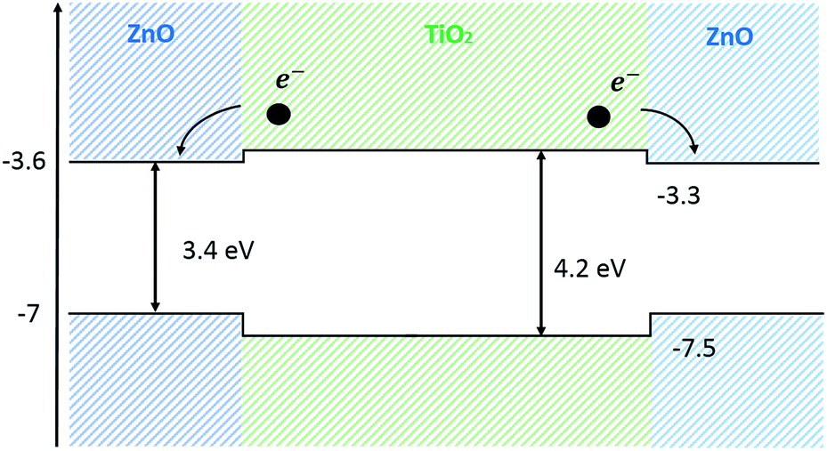 | ||
| Fig. 13 A schematic diagram of an isolated quantum well between ZnO and TiO2. | ||
5 Conclusion
In conclusion, we synthesized by ALD ZnO/TiO2 multilayers with a thickness lower than 80 nm. The effect of the deposition temperature (from 120 to 240 °C) on the electrical, optical, and structural properties of the films were investigated. In particular, the TZO films deposited at 200 °C showed the highest carrier concentration (∼5 × 1020 cm−3) and the lowest resistivity (∼3 × 10⁻³ Ω cm). All the TZO films resulted highly transparent in the visible range (>76%). Thanks to an accurate investigation through transmission electron microscopy we ruled out the well-assessed explanation of extrinsic doping mechanism of TCO. Indeed, if the Ti atoms had substituted the Zn ones, so to behave as donors, we would have detected TiO. The ELNES analyses differently excluded the presence of TiO, while revealing TiO2 nanodots (∼2 nm in diameter). The electrical and optical results could be explained by considering the formation of quantum wells in the semiconducting superlattice. The present results help in shedding light on the physical mechanisms responsible for the promising electrical properties of TZO, and could allow a better control of the n-type doping of TZO.Acknowledgements
The authors wish to thank Giuseppe Pantè (CNR-IMM) for fruitful technical assistance, Prof. Antonio Terrasi (University of Catania) and Dr. Paolo Longo (Gatan Inc.) for fruitful discussion. This research has been partially supported by the FP7 European project WATER (Grant Agreement 316082), and by the Italian MIUR project Beyond-Nano (PON a3_00363).References
- D. Sahu, S. Lin and J. Huang, Appl. Surf. Sci., 2006, 255, 7509 CrossRef
.
- D. S. Ginley, H. Hosono and D. C. Paine, in Handbook of Transparent Conductors, Springer, 2010 Search PubMed
- Y. F. Lan, W. C. Peng, Y. H. Lo and J. L. He, Mater. Res. Bull., 2009, 44, 1760 CrossRef CAS
- K. Ellmer, Nat. Photonics, 2012, 6, 809–817 CrossRef CAS
- S. S. Lin, J. L. Huang and P. Sajgalik, Surf. Coat. Technol., 2005, 191, 286 CrossRef CAS
- J. J. Lu, Y. M. Lu, S. I. Tasi, T. L. Hsiung, H. P. Wang and L. Y. Jang, Opt. Mater., 2007, 29, 1548 CrossRef CAS
- H. Chen, J. Ding and S. Ma, Superlattices Microstruct., 2011, 49, 176 CrossRef CAS
- R. E. Triambulo, H. Cheong, G. Lee, I. Yi and J. Park, J. Alloys Compd., 2015, 620, 340–349 CrossRef CAS
- Z.-Y. Ye, H.-L. Lu, Y. Geng, Y.-Z. Gu, Z.-Y. Xie, Y. Zhang, Q.-Q. Sun, S.-J. Ding and D. W. Zhang, Nanoscale Res. Lett., 2013, 8, 108 CrossRef PubMed
- K. Bergum, P.-A. Hansen, H. Fjellvåg and O. Nielsen, J. Alloys Compd., 2014, 616, 618 CrossRef CAS
- Z. Wan, W.-S. Kwack, W.-J. Lee, S.-I. I. Jang, H.-R. Kim, J.-W. Kim, K.-W. Jung, W.-J. Min, K.-S. Yu, S.-H. Park, E.-Y. Yun, J.-H. Kim and S.-H. Kwon, Mater. Res. Bull., 2014, 57, 23 CrossRef CAS
- K. Bergum, H. Fjellvåg and O. Nielsen, Appl. Surf. Sci., 2015, 332, 494 CrossRef CAS
- H.-P. Chang, F.-H. Wang, J.-C. Chao, C.-C. Huang and H.-W. Liu, Curr. Appl. Phys., 2011, 11, S185 CrossRef
- H. Chen, J. Ding and S. Ma, Superlattices Microstruct., 2011, 49, 176 CrossRef CAS
- Q. Huang, W. Shen, X. Fang, G. Chen, Y. Yang, J. Huang, R. Tan and W. Song, ACS Appl. Mater. Interfaces, 2015, 7, 4299 CAS
- T. Qiu, B. Luo, M. Liang, J. Ning, B. Wang, X. Li and L. Zhi, Carbon, 2015, 81, 232 CrossRef CAS
- Y. Duan, Y. Duan, P. Chen, Y. Tao, Y. Yang and Y. Zhao, Nanoscale Res. Lett., 2015, 10, 90 CrossRef PubMed
- N. Pinna and M. Knez, in Atomic Layer Deposition of Nanostructured Materials, Wiley-VCH, Weinheim, Germany, 2012 Search PubMed
- M. Ritala and J. Niinistö, ECS Trans., 2009, 25, 641 CAS
- A. Di Mauro, M. Cantarella, G. Nicotra, V. Privitera and G. Impellizzeri, Appl. Catal., B, 2016, 196, 68 CrossRef CAS
- Y. Wu, P. M. Hermkens, B. W. H. van de Loo, H. C. M. Knoops, S. E. Potts, M. A. Verheijen, F. Roozeboom and W. M. M. Kessels, J. Appl. Phys., 2013, 114, 024308 CrossRef
- D. Lee, H. Kim, J. Kwon, H. Choi, S. Kim and K. Kim, Adv. Funct. Mater., 2011, 21, 448 CrossRef CAS
- Y.-J. Choi and H.-H. Park, J. Mater. Chem. C, 2014, 2, 98–108 RSC
- E. Guziewicz, I. A. Kowalik, M. Godlewski, K. Kopalko, V. Osinniy, A. Wójcik, S. Yatsunenko, E. Łusakowska, W. Paszkowicz and M. Guziewicz, J. Appl. Phys., 2008, 103, 033515 CrossRef
- J. Su, in Optimization of TiO2 Thin Film Growth at Different Temperatures by Atomic Layer Deposition, Master's thesis, Aalto University, Finland, 2011, p. 39, https://aaltodoc.aalto.fi/handle/123456789/3790
- Q. Xie, Y.-L. Jiang, C. Detavernier, D. Deduytsche, R. L. Van Meirhaeghe, G.-P. Ru, B.-Z. Li and X.-P. Qu, J. Appl. Phys., 2007, 102, 083521 CrossRef
- J. T. Nam, J.-M. Kim, M.-K. Kim, H. Kim and W.-H. Kim, J. Korean Phys. Soc., 2011, 59, 452 CrossRef
- M. Thompson, see http://www.genplot.com for RUMP: Rutherford backscattering spectroscopy analysis package.
- J. Tauc, in Amorphous and Liquid Semiconductors, Plenum, New York, 1974, p. 175 Search PubMed
- B. D. Viezbicke, S. Patel, B. E. Davis and D. P. Birnie III, Phys. Status Solidi B, 2015, 8, 1700 CrossRef
- Ü. Özgür, Y. I. Alivov, C. Liu, A. Teke, M. A. Reshchikov, S. Doan, V. Avrutin, S.-J. Cho and H. Morkoç, J. Appl. Phys., 2005, 98, 041301 CrossRef
- I. Udom, M. K. Ram, E. K. Stefanakos, A. F. Hepp and D. Y. Goswami, Mater. Sci. Semicond. Process., 2013, 16, 2070 CrossRef CAS
- E. Burstein, Phys. Rev., 1954, 93, 632 CrossRef CAS
- J. Malm, E. Sahramo, J. Perälä, T. Sajavaara and M. Karppinen, Thin Solid Films, 2011, 519, 5319 CrossRef CAS
- G. Kothleitner, B. Schaffer, W. Grogger and F. Hofer, Microsc. Microanal., 2005, 11, 34 CrossRef
- G. Nicotra, Q. M. Ramasse, I. Deretzis, A. La Magna, C. Spinella and F. Giannazzo, ACS Nano, 2013, 7, 3045 CrossRef CAS PubMed
- G. Nicotra, R. A. Puglisi, S. Lombardo, C. Spinella, M. Vulpio, G. Ammendola, M. Bileci and C. Gerardi, J. Appl. Phys., 2004, 95, 2049 CrossRef CAS
- D. B. Williams and C. B. Carter, in Transmission Electron Microscopy, Springer, 2009, p. 747 Search PubMed
- E. Stoyanov, F. Langenhorst and G. Steinle-Neumann, Am. Mineral., 2007, 92, 577 CrossRef CAS
- G. Bertoni, E. Beyers, J. Verbeeck, M. Mertens, P. Cool, E. F. Vansant and G. Van Tendeloo, Ultramicroscopy, 2006, 106, 630 CrossRef CAS
- A. Gloter, C. Ewels, P. Umek, D. Arcon and C. Colliex, Phys. Rev. B: Condens. Matter Mater. Phys., 2009, 80, 035413–35421 CrossRef
- H. Lin, C. P. Huang, W. Li, C. Nib, S. I. Shah and Y.-H. Tseng, Appl. Catal., B, 2006, 68, 1 CrossRef CAS
- C. Pei and W. Leung, Sep. Purif. Technol., 2013, 114, 108–116 CrossRef CAS
- H. Peng, J. Li, S. Li and J. Xia, J. Phys. Chem. C, 2008, 112, 13964–13969 CAS
- A. N. Enyashin and G. Seifert, Phys. Status Solidi B, 2005, 242, 1361–1370 CrossRef CAS
| This journal is © The Royal Society of Chemistry 2016 |