
 Open Access Article
 This Open Access Article is licensed under a
 Creative Commons Attribution 3.0 Unported Licence
Haloplumbate salts as reagents for the non-aqueous electrodeposition of lead†
Philip N.
Bartlett
*,
Jennifer
Burt
,
Mahboba M.
Hasan
,
Andrew L.
Hector
,
William
Levason
,
Gillian
Reid
and
Peter W.
Richardson
Chemistry, University of Southampton, Southampton SO17 1BJ, UK. E-mail: P.N.Bartlett@soton.ac.uk
First published on 25th July 2016
Abstract
Cyclic voltammetry experiments on the Pb(II) salts, [PPh4][PbX3] (X = Cl, Br, I) in CH2Cl2 solution ([PPh4]X supporting electrolyte) at a Pt disk electrode show reproducible nucleation and stripping features consistent with reduction to elemental Pb. The reduction potential shifts to less cathodic from Cl (−0.40 V) → Br (−0.27 V) → I (−0.19 V vs. Ag/AgCl), in line with the Pb–X bond strengths decreasing. Potentiostatic electrodeposition using [PPh4][PbCl3] in CH2Cl2 leads to growth of a thin film of crystalline Pb onto planar TiN electrodes, confirmed by SEM, EDX and XRD analysis. Electrodeposition under similar conditions onto a planar Au electrode leads to deposition of elemental Pb, accompanied by some alloying at the substrate/film interface, with XRD analysis confirming the formation of AuPb2 and AuPb3. Transferring the [PPh4][PbCl3] reagent into supercritical CH2F2 (17.5 MPa and 360 K) containing [PPh4]Cl led to very limited solubility of the Pb reagent; using [NnBu4]Cl as a supporting electrolyte caused an increase in solubility, although still lower than in liquid CH2Cl2. Cyclic voltammetry experiments (Pt disk) using this electrolyte also show voltammetry consistent with Pb deposition, however the low solubility of the lead salt in scCH2F2 meant that electrodeposition onto a planar TiN substrate was not possible.
Introduction
The group 14 elements have long been important to the electronics industry. Since the first experimental observation of transistor action in n-type polycrystalline germanium in 1947, and subsequently in polycrystalline silicon, both of these semiconductor elements have remained fundamental to transistor technology and integrated circuitry.1 Meanwhile, graphene has recently emerged as a highly attractive material for numerous applications, including electronics, sensors and energy storage devices.2 Though used in various compound semiconductors (e.g. SnTe, PbTe and PbSnTe),3 the heavier group 14 elements, tin and lead, have received considerably less attention, although recent work has predicted new and exciting properties for these elements at the extreme nanoscale.4,5 For example, a theoretical study4 has predicted that α-tin will undergo a semimetal to semiconductor transition in nanowires with diameters less than ∼4 nm.The stable phase of lead is face centred cubic and metallic. Bulk lead is ductile, soft, highly malleable, has a high density and is a relatively poor electrical conductor.6 Bulk lead is an elementary superconductor below Tc = 7.2 K and so there has been a lot of interest in investigating and tailoring its superconducting behaviour at the nanoscale. Lead nanowires with diameters of ∼5 nm, synthesised using a template-assisted chemical vapour deposition (CVD) approach, have been shown to increase the Tc by 3–4 K above that of bulk Pb, while the upper critical field was almost two hundred times higher.7 Other reported methods of fabricating Pb nanowires (of varying crystallinities and with diameters typically >20 nm) include pressure casting into templates,8 template-assisted electrodeposition from aqueous electrolytes9–11 and solution phase synthesis involving the thermal decomposition of a lead precursor salt.12 Lead also forms important compound semiconductors; the narrow band gap binary semiconductors PbS, PbSe and PbTe have potential uses in sensors, infrared photodetectors, solar photovoltaics and thermoelectric devices. Nanowires of these materials show improved carrier mobilities, larger absorption cross sections and better absorption and emission polarisation sensitivities.13 A field effect transistor has been fabricated using a single PbTe nanowire.14
Previously, we reported versatile precursor systems for the electrodeposition of several main-group metals from both liquid dichloromethane15 and supercritical difluoromethane (scCH2F2).16 Non-aqueous solvents such as these offer several advantages for the electrodeposition of complex nanostructured materials over conventional aqueous electrolytes. These include: (i) the use of a much wider range of reagents which can be tailored to the application; (ii) access to more reactive alloy compositions; (iii) a wider electrochemical window, enabling the deposition of reactive materials; and (iv) access to higher temperature electrodeposition.
Studies on halometallate complexes of Ge(II) and Ge(IV) in CH2Cl2 have revealed that the reduction potential is more accessible (less cathodic) for the lower oxidation state17 and hence Pb(II) compounds would appear to be promising candidates for the non-aqueous electrodeposition of lead. Coordinatively saturated reagents can be preferable for electrodeposition since they can simplify the solution speciation, however, Pb(II) tends to form complexes with large and varying coordination numbers that are very labile in solution, making it difficult to design a precursor that is coordinatively saturated. We therefore chose to keep the systems as simple as possible, using well-defined halometallate salts incorporating organic cations to aid solubility in the low dielectric solvent.
Previous studies15 have shown that p-block halometallates can be readily synthesised in high yields and purity, are easily handled and are stable at high temperatures. They typically show a high solubility and stability in organic solvents, allowing high-concentration electrolytes to be prepared. By using well-defined molecular species it is easy to control the speciation in solution. Furthermore, the tetrabutylammonium chlorometallate salts exist for a wide range of the p-block elements, presenting the prospect of co-deposition from these mutually compatible reagents to form compound semiconductors and alloys. Investigations into the electrochemistry of [NnBu4][MCl4] (M = In, Sb, Bi) and [NnBu4]2[MCl6] (M = Se, Te) in CH2Cl2, using [NnBu4]Cl as the supporting electrolyte, found that they form stable and reproducible electrochemical systems from which the element can be electrodeposited.15 Due to the poor solubility of the Pb(II) halides in organic solvents,18 work with lead has focused on halometallate salts with solubilising cations, specifically using the [PPh4]+ cation.
Results and discussion
The structural chemistry of the lead(II) halides is complex and varied due to the stereochemical activity (or not) of the lone pair and their tendency to polymerise in the solid state.19 PbCl2 and PbBr2 are essentially isostructural, with a distorted nine-coordinate metal centre best described as [7 + 2] coordination, while PbI2 has the CdI2 hexagonal layer lattice structure.17 Though formation of the halometallate anions in situ from MX2 may be possible due to the large excess of X− ions in solution provided by the electrolyte, the poor solubility of PbX2 in CH2Cl2 means that the more stable and soluble [NnBu4]+ or [PPh4]+ salts are easier to manipulate.The Pb(II) halometallate precursors were synthesised using PbX2 and either [NnBu4]X or [PPh4]X in a dry solvent under an inert atmosphere.
While the crystal structure of [NnBu4][PbI3] is known,20,21 attempts to synthesise the salt based on the reported method (using a 1![[thin space (1/6-em)]](https://www.rsc.org/images/entities/char_2009.gif) :1:1 molar ratio of PbI2, NaI and [NnBu4][PF6] in acetone) resulted in the isolation of [NnBu4]8[Pb18I44] as a yellow powder,18 confirmed by microanalysis. Attempts to make [NnBu4][PbCl3] using either PbCl2 or Pb(NO3)2 as the lead source were unsuccessful, and so the [PPh4]+ ion was selected as an alternative cation as its solubilising properties in organic solvents are well known and a number of lead(II) halide salts have already been isolated.22–25
:1:1 molar ratio of PbI2, NaI and [NnBu4][PF6] in acetone) resulted in the isolation of [NnBu4]8[Pb18I44] as a yellow powder,18 confirmed by microanalysis. Attempts to make [NnBu4][PbCl3] using either PbCl2 or Pb(NO3)2 as the lead source were unsuccessful, and so the [PPh4]+ ion was selected as an alternative cation as its solubilising properties in organic solvents are well known and a number of lead(II) halide salts have already been isolated.22–25
The reactions of PbX2 and [PPh4]X (X = Cl, Br, I) in a 1:1 molar ratio using CH3CN as the solvent resulted in the formation of [PPh4][PbCl3]·CH3CN, [PPh4][PbBr3] and [PPh4]2[Pb2I6] as white or yellow powders. Unit cell determinations on single crystals of both [PPh4][PbCl3]·CH3CN and [PPh4]2[Pb2I6] were consistent with the reported structures, the former anion containing [PbCl3]− groups associated into chains via asymmetric (μ-Cl)2 chloro-bridges to give a distorted square pyramidal Pb(II) centre,20 while the latter anion is a discrete [Pb2I6]2− dimer where the Pb(II) centres have a distorted seesaw coordination geometry.22 The crystal structure of [PPh4][PbBr3] reveals discrete cations and (μ-Br)3 bromo-bridged chain polymer anions (Fig. 1). The Pb(II) centres have near-ideal octahedral coordination geometries (suggesting that the lone pair on the lead is stereochemically inactive) with a small range of Pb–Br bond lengths (2.9823(6)–3.0416(8) Å). The related compound, [PPh4]2[Pb3Br8], formed by reacting [PPh4]Br and PbBr2 in a 1:1 ratio in CH3CN at 75 °C, contains both distorted tetrahedral and octahedral Pb(II) centres, the latter of which have very similar bond lengths and angles to the Pb(II) centres in [PPh4][PbBr3].21
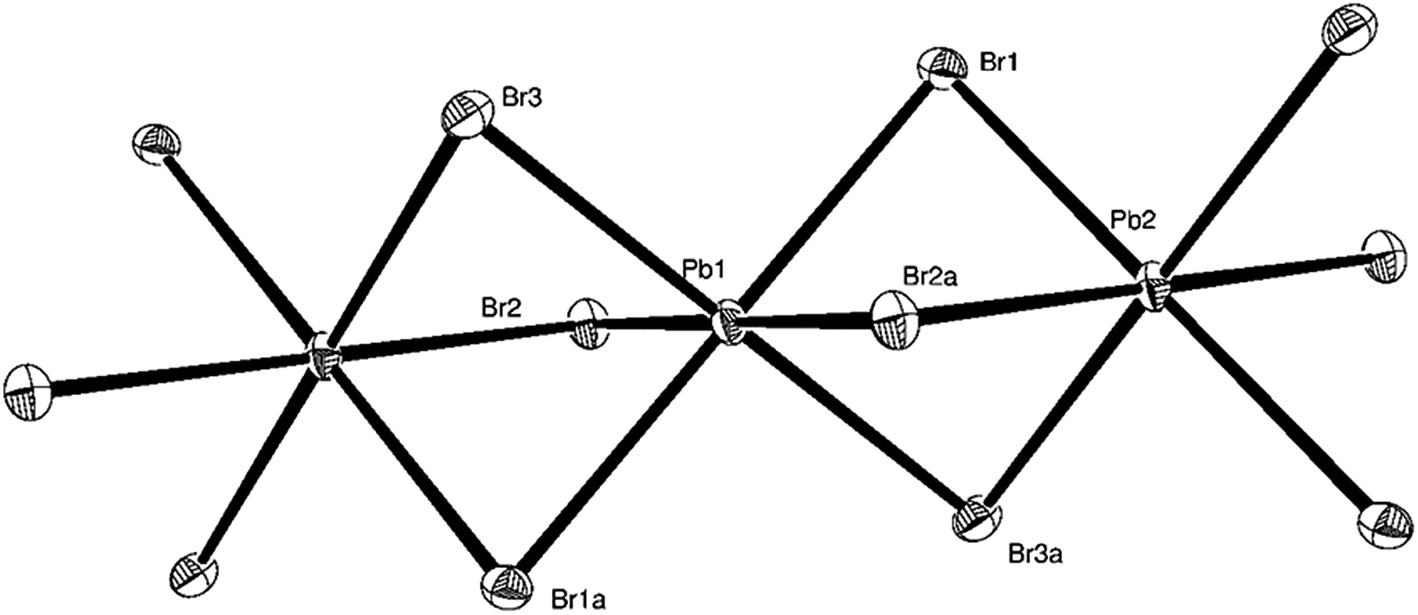 | ||
| Fig. 1 The structure of a portion of the chain polymer anion present in [PPh4][PbBr3] showing the atom labelling scheme. Ellipsoids are drawn at the 50% probability level. Symmetry operation: a = −x, −y, −z. Selected bond lengths (Å) and angles (°): Pb1–Br1 = 3.0416(8), Pb1–Br2 = 3.0332(8), Pb1–Br3 = 2.9823(6), Pb2–Br1 = 3.0179(7), Pb2–Br2a = 3.0176(6), Pb2–Br3a = 3.0296(7), Br1–Pb1–Br2 = 92.89(2), Br1–Pb1–Br3 = 96.094(16), Br2–Pb1–Br3 = 88.18(2), Br1–Pb1–Br2a = 87.11(2), Br1–Pb1–Br3a = 83.906(16), Br2–Pb1–Br3a = 91.82(2), Br1–Pb2–Br2a = 87.82(2), Br1–Pb2–Br3a = 83.51(2), Br2a–Pb2–Br3a = 87.60(2). | ||
No resonance could be found for the haloplumbate salts using 207Pb NMR spectroscopy in CH2Cl2, even with the addition of excess [PPh4]X. However, given the dissociative nature of Pb(II) compounds,26 the solution speciation of [PPh4][PbX3] is likely to involve simple, possibly mononuclear species, which are in rapid equilibrium.
Cyclic voltammetry and deposition studies were then performed on the Pb reagents in dry CH2Cl2 in order to evaluate their electrochemical properties. The supporting electrolyte used was [PPh4]X (where X matches the halogen present in the precursor) to avoid unnecessary complications through the introduction of other ions into the system, as X− is expected to be liberated during the reduction of the halometallate precursor.
To allow the efficient exclusion of air and moisture, the electrolyte preparation and electrochemical experiments were performed in a N2-filled glove box. The electrochemical experiments in CH2Cl2 were performed at room temperature using a three-electrode system in a single compartment electrochemical cell. A Pt gauze was used as the counter electrode, with a Ag/AgCl reference electrode (in 0.1 M [NnBu4]Cl in CH2Cl2). For the cyclic voltammetry experiments, the freshly polished working electrode used was a platinum (Pt, 0.5 mm diameter), gold (Au, 1.0 mm diameter) or glassy carbon (GC, 3.0 mm diameter) disk electrode. The cyclic voltammograms were recorded by starting at the open circuit potential and initially scanning negative to explore the metal reduction process first. Films of Pb were deposited potentiostatically onto planar gold or titanium nitride (TiN) slide electrodes. The latter is of interest because TiN is regularly used in electronic applications as a conductive barrier layer between metallic contacts and semiconductors.
Cyclic voltammetry studies of [PPh4][PbX3] in CH2Cl2
Due to the modest solubility of the lead(II) precursors in CH2Cl2, to ensure a homogeneous solution, an electrolyte containing 0.5 mM [PPh4][PbCl3] and 100 mM [PPh4]Cl in CH2Cl2 was prepared to investigate the electrochemical properties of the chlorometallate salt. The potential window available when [PPh4]Cl is used as the supporting electrolyte was established to be between −1.0 and +1.25 V vs. Ag/AgCl. Cyclic voltammograms recorded at a Pt disk working electrode (Fig. 2) reveal very reproducible features, with a well-defined nucleation loop and stripping peak. Once the nucleation overpotential is reached the deposition onset is very steep and peaks almost straightaway; subsequent deposition behaviour is diffusion limited. The deposition onset, peak deposition current and stripping onset for the scan recorded at 50 mV s−1 occur at −0.39 V, −0.40 V and −0.34 V. Comparable voltammograms were recorded with a GC disk working electrode at a scan rate of 50 mV s−1, with the deposition onset, peak deposition current and stripping onset occurring at −0.39 V, −0.43 V and −0.34 V. | ||
| Fig. 2 Cyclic voltammograms of 0.5 mM [PPh4][PbCl3] in CH2Cl2 as a function of scan rate, recorded at a 0.5 mm diameter Pt disk. The supporting electrolyte used was 100 mM [PPh4]Cl. | ||
Extra features were observed on cyclic voltammograms recorded at an Au disk working electrode (Fig. 3). The first scan on a fresh electrode shows two reduction waves, while on subsequent scans a third reduction process is also evident, presumably because the electrode surface has been altered. The underpotential deposition of Pb on gold in various media has been extensively studied,27,28 while Pb is also known to form three Au alloys, Au2Pb, AuPb2 and AuPb3.29 The charge associated with the first peak on the first scan (2.8 μC) is comparable to the theoretical charge required for the formation of a Pb monolayer on the Au electrode (2.0 μC) based on the literature,27 suggesting an underpotential deposition process. The peak deposition current for bulk Pb occurs at −0.38 V, while the deposition and stripping onset are both at −0.34 V.
 | ||
| Fig. 3 Cyclic voltammograms of 0.5 mM [PPh4][PbCl3]·CH3CN in CH2Cl2 recorded at a 1.0 mm diameter Au disk. The supporting electrolyte used was 100 mM [PPh4]Cl and the potential scan rate was 50 mV s−1. | ||
The effect of systematically changing the halide on the cyclic voltammetry of the tetraphenylphosphonium Pb(II) salts in CH2Cl2, recorded at Pt disk working electrodes, was investigated. Cyclic voltammograms (Fig. 4) recorded for [PPh4][PbBr3] and [PPh4]2[Pb2I6], using the corresponding [PPh4]X as the supporting electrolyte, showed similar metal deposition and stripping features as recorded for [PPh4][PbCl3], with the deposition onset, peak deposition current and stripping onset at −0.25 V, −0.27 V and −0.23 V for [PPh4][PbBr3] and at −0.17 V, −0.19 V and −0.14 V for [PPh4]2[Pb2I6]. Importantly, it becomes clear that when X changes Cl → Br → I the Pb(II) to Pb(0) reduction potential becomes more positive, with the reduction of the [Pb2I6]2− ion the most accessible. A similar trend has been observed for [EMIM][GeX3] (X = Cl, Br, I; EMIM = ethylmethylimidazolium) complexes in CH2Cl2,17 most likely reflecting the variation in the Ge/Pb–X bond strengths.
 | ||
| Fig. 4 Cyclic voltammograms of [PPh4][PbX3] (X = Cl, Br, I) in CH2Cl2 recorded at a 0.5 mm diameter Pt disk. The composition of each electrolyte system was 0.5 mM (based on Pb content) of (i) [PPh4][PbCl3], (ii) [PPh4][PbBr3] and (iii) [PPh4]2[Pb2I6] with 100 mM [PPh4]X. The potential scan rate was 50 mV s−1. | ||
Cyclic voltammetry studies of [PPh4][PbCl3] in scCH2F2
Electrochemistry of [PPh4][PbCl3] in scCH2F2 using the [PPh4]Cl electrolyte was unsuccessful due to the low solubility of the background electrolyte in the supercritical fluid. Instead, experiments were performed with [NnBu4]Cl as the supporting electrolyte, as this system showed good electrochemical behaviour in CH2Cl2 (ESI†). The voltammeteric characteristics of the [PPh4][PbCl3] precursor in scCH2F2 at 17.5 MPa and 360 K at a Pt disk are presented in Fig. 5. The voltammogram displays typical electrodeposition features, including a well-defined nucleation loop with an onset potential at −0.60 V, and an anodic stripping peak that has an onset at −0.50 V and a peak at −0.35 V. The noise in the limiting current region (cathodic of −0.5 V) is due to rapid convection in the supercritical fluid. | ||
| Fig. 5 Cyclic voltammetry of 2 mM [PPh4][PbCl3] + 50 mM [NnBu4]Cl at a Pt disk electrode (surface area 1.963 × 10⁻³ cm2) in scCH2F2 (17.5 MPa, 360 K). The potential scan rate was 50 mV s−1. | ||
Electrodeposition of lead from CH2Cl2 solution
The potentiostatic electrodeposition of Pb in CH2Cl2 was investigated on Au and TiN slides using an electrolyte containing 0.5 mM [PPh4][PbCl3] and 100 mM [PPh4]Cl. Details of the parameters involved in both deposition experiments are given in Table 1.| Au slide | TiN slide | |
|---|---|---|
| Deposition potential (V) | −0.6 | −1.0 |
| Deposition time (s) | 3600 | 3600 |
| Area of electrode (cm2) | 0.25 | 0.30 |
| Charge passed (C) | 0.10 | 0.12 |
| Estimated deposit thickness (μm) | 0.39 | 0.38 |
The deposited dark grey films on the electrodes were gently washed by immersing the films into CH2Cl2 before being analysed by SEM, EDX and XRD. SEM images of the deposited Pb films (Fig. 6) show that the material on the Au slide is formed of individual crystallites of differing sizes spread fairly uniformly across the electrode surface, while the crystallite morphology on the TiN slide is more regular. EDX analysis shows Pb as the dominant peak, but, unsurprisingly, given the thinness of the deposited films, Au or Ti and Si peaks from the Au or TiN substrate were also evident. No chloride was observed in any of the EDX spectra recorded.
 | ||
| Fig. 6 SEM micrographs of Pb electrodeposited on planar electrodes in CH2Cl2. The substrates and magnifications used are (a) Au, ×2000 (scale bar = 10 μm), (b) Au, ×10000 (scale bar = 1 μm), (c) TiN, ×2000 (scale bar = 10 μm), (d) TiN, ×13000 (scale bar = 1 μm). | ||
Grazing incidence X-ray diffraction (GIXRD) data were collected on the films deposited on TiN and gold under the conditions shown in Table 1 to understand their phase behaviour. Symmetric (θ–θ2) scans were also collected to test for preferred orientation of the deposit, though none was found and these patterns contained strong substrate reflections.
The GIXRD pattern of the film deposited on TiN contained the expected fcc lead peaks and weak reflections due to the substrate and to a small quantity of PbO, presumably due to air oxidation of the film. Rietveld analysis of the pattern (Fig. 7a, Rwp = 12.2% and Rp = 9.0%) resulted in a lead lattice parameter of a = 4.9643(3) Å (Lit.30 4.950(1) Å) and thermal parameter of Uiso = 0.0316(12) Å2. The films contained 9.5(6)% PbO (litharge structure31), although this is likely to be due to surface oxidation and hence the refined figure is probably higher than the real content due to the surface enhancement provided by the grazing incidence geometry. Some weak reflections due to the TiN substrate were also observed.
 | ||
| Fig. 7 Rietveld fits to the GIXRD patterns of Pb films deposited on (a) TiN or (b) gold. In each plot the crosses mark data points, the top continuous line the fit, tick marks the allowed reflection positions and the bottom continuous line the difference. In (a) the upper tick marks are for PbO and the lower for Pb; in (b) the sequence is AuPb3 (top), Au, AuPb2, Pb (bottom). Peaks due to phases not included in the fit are marked. | ||
The film deposited on gold also underwent some alloying with the gold, and strong alloy reflections in the symmetric scans suggested this was mainly at the substrate–film interface. The formation of these alloy phases may explain the additional peaks observed in the voltammetry on gold disk electrodes (Fig. 3). Rietveld analysis of the GIXRD pattern (Fig. 7b, Rwp = 16.0% and Rp = 12.6%) provided a lead lattice parameter of a = 4.9631(4) Å (Lit.30 4.950(1) Å), very similar to that found on TiN, and thermal parameter of Uiso = 0.0460(18) Å2. The two alloy phases were included in the fit and found to be 36.4(7)% AuPb2 (I4/mcm,32a = 7.36 Å and c = 5.67 Å) and 10.8(4)% AuPb3 (I![[4 with combining macron]](https://www.rsc.org/images/entities/char_0034_0304.gif) 2m,33a = 12.04 and c = 5.94 Å) by mass, although these may be underestimates as they are likely to be mainly present at the substrate/film interface. Peaks due to the gold substrate were also modelled, but due to preferred orientation of the substrate this was done in Le Bail mode. A weak reflection due to PbO was also observed and is marked in Fig. 3b.
2m,33a = 12.04 and c = 5.94 Å) by mass, although these may be underestimates as they are likely to be mainly present at the substrate/film interface. Peaks due to the gold substrate were also modelled, but due to preferred orientation of the substrate this was done in Le Bail mode. A weak reflection due to PbO was also observed and is marked in Fig. 3b.
The precursor [PPh4][PbCl3] has been shown to have a favourable Pb(II) to Pb(0) deposition potential and shows good, reproducible voltammetric behaviour in CH2Cl2, with thin films of Pb having been successfully electrodeposited on TiN substrates. However attempts to deposit thin films of Pb on TiN from scCH2F2 using [NnBu4]Cl as the supporting electrolyte were unsuccessful, probably because of the rather low solubility of the reagent in the low dielectric supercritical fluid.
Conclusions
The series of tetraphenylphosphonium halometallate precursors for the electrodeposition of lead, [PPh4][PbX3] (X = Cl, Br, I), has been synthesised and characterised, including by single crystal X-ray diffraction. Using [PPh4]X as the supporting electrolyte, the deposition voltammetry of the precursors has been well characterised in CH2Cl2 solution and Pb has been successfully electrodeposited on planar Au and TiN electrodes from [PPh4][PbCl3]·CH3CN in CH2Cl2. The reduction potentials for the Group 14 M(II) → M(0) using [MX3]− salts (M = Ge, Pb; X = Cl, Br, I) become less cathodic and therefore more accessible as both groups 14 and 17 are descended. Electrochemical studies of the [PPh4][PbCl3] salt in scCH2F2 found that in [PPh4]Cl electrolyte the solubility was too low to record voltammetry but with [NnBu4]Cl supporting electrolyte lead can be deposited and stripped at a platinum disc electrode.The results from this work indicate that lead may be readily electrodeposited from the haloplumbate salts using liquid CH2Cl2. This broadens further the range of p-block elements accessible using these solvents, and may also offer the potential for electrodeposition of lead alloys and/or binary semiconductors, such as lead telluride (by combining [PbCl3]− and [TeCl6]2− in a single electrolyte bath in CH2Cl2), in a similar manner to that which we used recently for the electrodeposition of functional Ge2Sb2Te5 phase change memory.34
Experimental
Reactions were carried out under a dry dinitrogen atmosphere using Schlenk line and glove box techniques. The products were stored, and spectroscopic samples prepared, in a N2-filled glove box. Solvents were dried and degassed prior to use. CH3CN and CH2Cl2 were distilled over CaH2; the former was stored over molecular sieves (4 Å). The lead dihalides were purchased from Sigma-Aldrich and used as received.IR spectra were recorded as Nujol mulls between CsI plates using a Perkin Elmer Spectrum 100 spectrometer over the range 4000–200 cm−1. NMR spectra were recorded using a Bruker AVII400 or AVIIIHD400 spectrometer. 1H spectra were referenced to the residual solvent reference and 31P{1H} to external 85% H3PO4. Microanalytical measurements were performed by London Metropolitan University.
Single crystal X-ray data were collected using a Rigaku AFC12 goniometer equipped with an enhanced sensitivity (HG) Saturn724+ detector mounted at the window of an FR-E+ SuperBright molybdenum (λ = 0.71073 Å) rotating anode generator with VHF Varimax optics (70 μm focus), with the crystal held at 100 K (N2 cryostream). Structure solution and refinement were performed with SHELX(S/L)97,35 with H atoms bonded to C placed in calculated positions using default C–H distances. Crystallographic parameters are presented in Table 2 and the structure has been assigned CCDC number 1480713.
| a Common items: T = 100 K; wavelength (Mo-Kα) = 0.71073 Å; θ(max) = 27.5°. b R 1 = Σ||Fo| − |Fc||/Σ|Fo|; wR2 = [Σw(Fo2 − Fc2)2/ΣwFo4]1/2. | |
|---|---|
| Compound | [PPh4][PbBr3] |
| Formula | C24H20Br3PPb |
| M | 786.29 |
| Crystal system | Triclinic |
| Space group (no.) |
P![[1 with combining macron]](https://www.rsc.org/images/entities/char_0031_0304.gif) (2) (2) |
| a/Å | 7.402(2) |
| b/Å | 12.192(3) |
| c/Å | 14.520(4) |
| α/° | 69.065(9) |
| β/° | 86.790(12) |
| γ/° | 73.933(9) |
| U/Å3 | 1174.7(5) |
| Z | 2 |
| μ(Mo-Kα)/mm−1 | 12.361 |
| F(000) | 732 |
| Total no. reflns | 10181 |
| R int | 0.033 |
| Unique reflns | 5254 |
| No. of params, restraints | 265, 0 |
| R 1, wR2 [I > 2σ(I)]b | 0.020, 0.041 |
| R 1, wR2 (all data) | 0.024, 0.042 |
[PPh4][PbCl3]·CH3CN
To a suspension of PbCl2 (0.101 g, 0.36 mmol) in CH3CN (20 mL) was added [PPh4]Cl (0.138 g, 0.37 mmol) to form a colourless solution. The reaction was stirred for 18 h, then the solvent volume was reduced to about 4 mL in vacuo whereupon a white solid precipitated out. The white powder was isolated by filtration and dried in vacuo. Meanwhile colourless crystals suitable for single crystal X-ray diffraction study grew in the filtrate which was stored at −18 °C. These were isolated by filtration and dried in vacuo to afford a second crop of the product. The overall yield was 0.133 g (53%). Anal. calc. for C26H23Cl3NPPb: C, 45.0; H, 3.3; N, 2.0. Found: C, 44.9; H, 3.3; N, 2.0%. 1H NMR (CD2Cl2, 295 K): δ = 1.97 (s, CH3CN), 7.60–7.95 (m, C6H5). 31P{1H} NMR (CD2Cl2, 295 K): δ = 23.9 (s).[PPh4][PbBr3]
To PbBr2 (0.100 g, 0.27 mmol) and [PPh4]Br (0.115 g, 0.27 mmol) was added CH3CN (20 mL) to initially form a suspension. Upon stirring for 0.5 h all the solid had dissolved to give a colourless solution. The reaction was stirred for 17 h, then the solvent volume was reduced to about 5 mL in vacuo whereupon a white solid precipitated out. The white powder was isolated by filtration and dried in vacuo. Meanwhile colourless needle-like crystals grew in the filtrate which was stored at −18 °C. These were isolated by filtration and dried in vacuo to afford a second crop of the product. The overall yield was 0.079 g (37%). Anal. calc. for C24H20Br3PPb: C, 36.7; H, 2.6. Found: C, 36.8; H, 2.5%. 1H NMR (CD2Cl2, 295 K): δ = 7.60–7.95 (m, C6H5). 31P{1H} NMR (CD2Cl2, 295 K): δ = 23.9 (s). A very large colourless crystal suitable for single crystal X-ray diffraction study grew upon allowing a portion of the filtrate to evaporate.[PPh4]2[Pb2I6]
To PbI2 (0.227 g, 0.49 mmol) was added CH3CN (20 mL) resulting in a yellow solution with evidence of some undissolved solid which did not change upon stirring for 0.5 h. To this was added [PPh4]I (0.229 g, 0.49 mmol) which immediately led to the precipitation of a large amount of yellow solid. The reaction was stirred for 18 h, then the yellow powder was isolated by filtration and dried in vacuo. Yield: 0.299 g (66%). Anal. calc. for C48H40I6P2Pb2: C, 31.1; H, 2.2. Found: C, 30.9; H, 2.1%. 1H NMR (CD2Cl2, 295 K): δ = 7.60–7.95 (m, C6H5). 31P{1H} NMR (CD2Cl2, 295 K): δ = 23.9 (s). Yellow crystals suitable for single crystal X-ray diffraction study grew from a solution of the powder in CH2Cl2.Electrochemical measurements in CH2Cl2
The electrolyte preparation and electrochemical experiments in dry CH2Cl2 were carried out under a dry dinitrogen atmosphere inside a glove box. The electrochemical measurements were performed at room temperature using a three-electrode system in a one-compartment electrochemical cell that had a volume of 10 mL. A Pt gauze was used as the counter electrode, and an Ag/AgCl electrode (in 0.1 mol dm−1 [NnBu4]Cl in CH2Cl2) was used as the reference electrode. For voltammetric characterisation of the compounds the working electrodes used were platinum (0.5 mm diameter), gold (1.0 mm diameter) or glassy carbon (3.0 mm diameter) disk electrodes sealed in glass. These were polished with alumina paste (1 and 0.3 μm) on microfiber polishing cloth (Buehler). Films were deposited potentiostatically onto either gold or TiN slides. The evaporated gold slides consisted of microscope slides coated with a 15 nm chromium adhesion layer and 100 nm of gold. Details of how the TiN on Si slides were fabricated can be found in the literature.16 An Autolab PGStat302 potentiostat and Autolab NOVA software was used to conduct the electrochemical measurements and data logging. After deposition the films were washed by holding them in a static solution of CH2Cl2 for 30 seconds.Electrochemical measurements in scCH2F2
Supercritical fluid electrochemical studies were performed in a stainless steel high-pressure cell, the details of which have been described in previous publications.36,37 The [PPh4][PbCl3] and [NnBu4]Cl complexes were transferred into the cell inside a nitrogen-purged glove box. Once sealed, the cell was removed from the glove box, connected to a high-pressure rig and heated to the desired temperature using a band heater under PID (proportional–integral–derivative) control. The scCH2F2 was then introduced using a specialized carbon dioxide pump (PU-1580-CO2, JASCO) until the desired pressure was achieved. To ensure that the solution was homogeneous, the system was stirred during pumping using a magnetic stirrer. Stirring was stopped at least 5 minutes prior to electrochemical measurements. All experiments were carried out at 17.2 MPa and 358 K. The electrochemical experiments were performed using a three-electrode system. A platinum mesh served as the counter electrode, and a 0.5 mm diameter platinum disk operated as a pseudo-reference electrode. A 0.5 mm diameter (surface area 1.963 × 10⁻³ cm2) platinum disk sealed in polyether ether ketone (PEEK) was used as the working electrode for the voltammeteric characterisation. The Pt disk was polished to a mirror finish with alumina paste (1.0 and 0.3 μm) on microfibre polishing cloth. Cyclic voltammetry measurements were recorded at potential sweep rates of 50 mV s−1.Characterisation of electrodeposited lead
Electrodeposited films were investigated using SEM, EDX and XRD. A Jeol JSM 6500F field emission gun scanning electron microscope (FEG-SEM) equipped with an Oxford Instruments EDX detector was used for the SEM and EDX analyses of electrodeposited films, for which an accelerating voltage of 20 keV was employed.XRD patterns of lead films were collected using a Riguku Smartlab Thin Film diffractometer with a 0.1 mm parallel line of Cu-Kα X-rays, 5° Soller slits and a DTex250 1D detector. Grazing incidence patterns were collected with a 1° incidence angle. Data were initially compared with databases using the Rigaku PDXL package, then refined using the GSAS package38 and models from ICSD.39
Acknowledgements
We thank EPSRC for support (EP/I010890/1, EP/K00509X/1, EP/K009877/1 and EP/K039466/1). The SCFED Project (http://www.scfed.net) is a multidisciplinary collaboration of British universities investigating the fundamental and applied aspects of supercritical fluids. PNB gratefully acknowledges receipt of a Wolfson Research Merit Award.References
- H. R. Huff, AIP Conf. Proc., 2003, 683, 3–39 CrossRef.
- K. Rana, J. Singh and J.-H. Ahn, J. Mater. Chem. C, 2014, 2, 2646–2656 RSC.
- J. O. Dimmock, I. Melngailis and A. J. Strauss, Phys. Rev. Lett., 1966, 16, 1193–1196 CrossRef CAS.
- L. Ansari, G. Fagas, J.-P. Colinge and J. C. Greer, Nano Lett., 2012, 12, 2222–2227 CrossRef CAS PubMed.
- N. G. Hörmann, A. Gross, J. Rohrer and P. Kaghazchi, Appl. Phys. Lett., 2015, 107, 123101 CrossRef.
- Lead: Chemistry, Analytical Aspects, Environmental Impact and Health Effects, ed. J. S. Casas and J. Sordo, Elsevier B. V., Amsterdam, 2006 Search PubMed.
- M. He, C. H. Wong, P. L. Tse, Y. Zheng, H. Zhang, F. L. Y. Lam, P. Sheng, X. Hu and R. Lortz, ACS Nano, 2013, 7, 4187–4193 CrossRef CAS PubMed.
- C. Jung-Hsuan, L. Shen-Chuan, C. Chuen-Guang and L. Tzeng-Feng, Jpn. J. Appl. Phys., 2008, 47, 4815–4819 CrossRef.
- G. Yi and W. Schwarzacher, Appl. Phys. Lett., 1999, 74, 1746–1748 CrossRef CAS.
- A. A. Zhukov, E. T. Filby, M. A. Ghanem, P. N. Bartlett and P. A. J. de Groot, Phys. C, 2004, 404, 455–459 CrossRef CAS.
- E. T. Filby, A. A. Zhukov, P. A. J. de Groot, M. A. Ghanem, P. N. Bartlett and V. V. Metlushko, Appl. Phys. Lett., 2006, 89, 092503 CrossRef.
- Y. Wang, T. Herricks and Y. Xia, Nano Lett., 2003, 3, 1163–1166 CrossRef CAS.
- A. C. Onicha, N. Petchsang, T. H. Kosel and M. Kuno, ACS Nano, 2012, 6, 2833–2843 CrossRef CAS PubMed.
- J. So Young, K. Han Sung, P. Jeunghee, J. Minkyung, K. Jinhee, L. Seung Hyun, R. Jong Wook and L. Wooyoung, Nanotechnology, 2009, 20, 415204 CrossRef PubMed.
- P. N. Bartlett, D. Cook, C. H. de Groot, A. L. Hector, R. Huang, A. Jolleys, G. P. Kissling, W. Levason, S. J. Pearce and G. Reid, RSC Adv., 2013, 3, 15645–15654 RSC.
- P. N. Bartlett, J. Burt, D. A. Cook, C. Y. Cummings, M. W. George, A. L. Hector, M. M. Hasan, J. Ke, W. Levason, D. Pugh, G. Reid, P. W. Richardson, D. C. Smith, J. Spencer, N. Suleiman and W. Zhang, Chem.–Eur. J., 2016, 22, 302–309 CrossRef CAS PubMed.
- P. N. Bartlett, C. Y. Cummings, W. Levason, D. Pugh and G. Reid, Chem.–Eur. J., 2014, 20, 5019–5027 CrossRef CAS PubMed.
- E. S. Claudio, H. A. Godwin and J. S. Magyar, Prog. Inorg. Chem., 2003, 51, 1–144 CAS.
- N. N. Greenwood and A. Earnshaw, Chemistry of the Elements, Butterworth-Heinemann, Oxford, 2nd edn, 1997 Search PubMed.
- H. Krautscheid and F. Vielsack, Angew. Chem., Int. Ed. Engl., 1995, 34, 2035–2037 CrossRef CAS.
- Y.-J. She, S.-P. Zhao, Z.-F. Tian and X.-M. Ren, Inorg. Chem. Commun., 2014, 46, 29–32 CrossRef CAS.
- W. Czado and U. Müller, Z. Anorg. Allg. Chem., 1998, 624, 925–926 CrossRef CAS.
- T. M. Klapotke, B. Krumm, K. Polborn and C. M. Rienicker, Z. Naturforsch., B: J. Chem. Sci., 2000, 55, 377–382 CAS.
- H. Krautscheid and F. Vielsack, Z. Anorg. Allg. Chem., 1999, 625, 562–566 CrossRef CAS.
- H. Krautscheid, J.-F. Lekieffre and J. Besinger, Z. Anorg. Allg. Chem., 1996, 622, 1781–1787 CrossRef.
- J. Parr, in Comprehensive Coordination Chemistry II, ed. J. A. McCleverty and T. J. Meyer, Elsevier, Oxford, 2004, vol. 3, p. 545 Search PubMed.
- B.-Y. Chang, E. Ahn and S.-M. Park, J. Phys. Chem. C, 2008, 112, 16902–16909 CAS.
- F.-X. Wang, G.-B. Pan, Y.-D. Liu and Y. Xiao, Chem. Phys. Lett., 2010, 488, 112–115 CrossRef CAS.
- A. Prince, Bull. Alloy Phase Diagrams, 1980, 1, 59–62 CrossRef.
- N. Bouad, L. Chapon, R. M. Marin-Ayral, F. Bouree-Vigneron and J. C. Tedenac, J. Solid State Chem., 2003, 173, 189–195 CrossRef CAS.
- P. Boher, P. Garnier, J. R. Gavarri and A. W. Hewat, J. Solid State Chem., 1985, 57, 343–350 CrossRef CAS.
- E. E. Havinga, H. Damsma and P. Hokkeling, J. Less-Common Met., 1972, 27, 169–186 CrossRef CAS.
- R. Wang and B. C. Giessen, Metall. Trans., 1971, 2, 2195–2197 CrossRef CAS.
- P. N. Bartlett, S. L. Benjamin, C. H. De Groot, A. L. Hector, R. Huang, A. Jolleys, G. P. Kissling, W. Levason, S. J. Pearce, G. Reid and Y. Wang, Mater. Horiz., 2015, 2, 420–426 RSC.
- G. Sheldrick, Acta Crystallogr., Sect. A: Found. Crystallogr., 2008, 64, 112–122 CrossRef CAS PubMed.
- J. Ke, W. Su, M. W. George, S. M. Howdle, D. Cook, M. Perdjon-Abel, P. N. Bartlett, W. Zhang, F. Cheng, W. Levason, G. Reid, D. Smith, J. Hyde, J. Wilson and P. Sazio, Proc. Natl. Acad. Sci. U. S. A., 2009, 106, 14768–14772 CrossRef CAS PubMed.
- D. Cook, P. N. Bartlett, W. Zhang, W. Levason, G. Reid, J. Ke, W. Su, M. W. George, J. Wilson, D. Smith, K. Mallik, E. Barrett and P. Sazio, Phys. Chem. Chem. Phys., 2010, 12, 11744–11752 RSC.
- (a) A. C. Larson and R. B. Von Dreele, Generalized Structure Analysis System (GSAS), Los Alamos National Laboratory Report LAUR, 2004, pp. 86–748 Search PubMed; (b) B. H. Toby, J. Appl. Crystallogr., 2001, 34, 210–213 CrossRef CAS.
- Inorganic Crystal Structure Database (Fiz Karlsruhe) accessed via the National Chemical Database Service hosted by the Royal Society of Chemistry.
Footnote |
| † Electronic supplementary information (ESI) available: Voltammetry of [PPh4][PbCl3] and [NnBu4]Cl in CH2Cl2 and chromoamperometry for Pb deposition and the cif file for the X-ray crystal structure. CCDC 1480713. For ESI and crystallographic data in CIF or other electronic format see DOI: 10.1039/c6ra12942k |
| This journal is © The Royal Society of Chemistry 2016 |