
Long-term stability of Si-organic hybrid solar cells with a thermally tunable graphene oxide platform†
Beo Deul Ryu‡
a,
Jung-Hwan Hyung‡ab,
Min Hana,
Gil-Sung Kima,
Nam Hanc,
Kang Bok Koa,
Ko Ku Kanga,
Tran Viet Cuongad and
Chang-Hee Hong*a
aSchool of Semiconductor and Chemical Engineering, Semiconductor Physics Research Center, Chonbuk National University, Jeonju, Jeollabuk-do 54896, Korea. E-mail: chhong@jbnu.ac.kr; Tel: +82 63-2702831
bDepartment of Nanosystem Research, National Nano Fab Center (NNFC), Daejeon, 305-701, Korea
cDepartment of Material Science and Engineering, Pohang University of Science and Technology (POSTECH), Pohang, Gyeongbuk 790-784, Korea
dNTT Hi-Tech Institute, Nguyen Tat Thanh University, 298-300 A Nguyen Tat Thanh Street, Ho Chi Minh City, Vietnam
First published on 22nd July 2016
Abstract
We demonstrated that a reduced graphene oxide (rGO) layer inserted between a poly(3,4-etylenedioxythiophene):poly(styrenesulfonate) (PEDOT:PSS) and Si interface improves the stability of Si-organic hybrid solar cells. Thermal reduction of a graphene oxide layer at different temperatures results in a change of water contact angle that is designed to eliminate the surface oxidation of the Si substrate. Higher temperatures generate a smaller aromatic sp2 domain size that changes the GO surface from hydrophilic to hydrophobic. Additionally, two-dimensional GO layers can serve as a barrier for both liquid and vapor permeation. Consequently, the PEDOT:PSS/Si device with a rGO passivation layer shows a significantly enhanced air-stability from the J–V characteristic under illumination during a one-month storage period. The application of rGO is a promising technique to extend the stability of Si-organic solar cells without an encapsulation process.
1. Introduction
Inorganic–organic solar cells based on silicon (Si) are currently under intensive investigation due to the unique advantages they offer compared with the traditional high temperature process p–n junction cells, such as easy fabrication, simple device structure, and potentially low-temperature process.1,2 The Si-organic solar cells combining the advantageous characteristics of crystalline Si and transparent conductive organic materials, such as poly(3,4-ethylene dioxythiophene):poly-styrenesulfonate (PEDOT:PSS), have emerged as promising candidates for cost-effective photovoltaic devices. The main functions of the organic layer are the following: (i) formation of a heterojunction with Si, (ii) a hole/electron transporting path, (iii) an optical window, and (iv) an antireflection coating.3–5 Over the past few years, considerable progress has been achieved in the study of Si-organic solar cells, and power conversion efficiencies (PCE) of over 10% have been reported by many groups.6–8 However, as the surface defects (i.e. microvoids) of PEDOT:PSS were always generated during the spin-coating process, the oxygen and moisture diffused through the PEDOT:PSS layer to form an insufficient oxide layer on Si substrate.9 As a result, the PCE of Si-organic solar cell gradually degrades during operation. To enhance the stability of Si-organic solar cell, previous studies have reported the usage of SiOx, MoO3, SiNx, and Al2O3 layers.8,10–12Recently, for the photovoltaic applications, graphene oxide (GO) has been adopted in organic solar cells as the hole transport layer (HTL).13–27 The GO sheets are exfoliated from graphite and dispersed in water to make the GO aqueous dispersion that has many advantages such as low cost, high yield, and processability. However, the PCE of organic solar cells with GO is highly sensitive to the thickness of GO layer because of its insulating properties. For the enhanced conductivity of GO, an insulating GO layer is easily tunable by chemical and thermal reduction processes to remove its oxygen functional groups, and the resulting layer is called reduced GO (rGO).28 Yang et al. demonstrated that treated GO with oxygen plasma was efficient in blocking electrons and collecting holes in organic solar cells.16 The work function of GO with the oxygen plasma treatment was higher than that of GO layer, which results in the increase of the hole mobility and the enhancement of hole extraction. Liu et al. indicated that the rGO reduced by thermal annealing (130 and 230 °C) enhanced the electrical properties in organic solar cells.23 Paci et al. mentioned that organic photovoltaic devices with the partially reduced GO (160 °C of annealing temperature) used as the HTL exhibited photovoltaic characteristics similar to the PEDOT:PSS-based devices but with a significant stability enhancement.24 So far, almost all reports have paid attention to improving the performance of Si-organic solar cell with the tunable physical properties of rGO.25,26 However, there is limited research regarding the effect of thermally annealed rGO on the long-term stability of Si-organic solar cells.
In this paper, we report the fabrication of package-free Si-organic solar cell with the use of rGO passivation layer. The coated GO layers on a Si substrate were changed to rGO layer by a thermal annealing process at temperatures of 700, 800, and 900 °C. Then, we observe the surface change of individual rGO layer by the water contact angle. The PEDOT:PSS/rGO/Si solar cell show long-term stability by current density–voltage and current–voltage characteristics in air ambient during a one-month storage period. We find that the rGO layer helps to prevent water molecules interaction in PEDOT:PSS/rGO/Si solar cell.
2. Experimental
2.1 GO synthesis
The GO was synthesized by using the modified Hummer's method.30 5 g of enlarged graphite and 500 mL of concentrated H2SO4 were mixed in a bottle to make a suspension. Then, 30 g of KMnO4 was slowly added and the resulting mixture was stirred for 2 h at 800 rpm. The mixture was subsequently diluted with 6 L of de-ionized water and thermally stabilized below 70 °C before slowly adding 15 mL of H2O2 (30 wt%) until active bubbles appeared, and the color of the suspension changed from dark brownish to yellow. The suspension was filtered and washed four times with 5 L of 10% HCl solution, followed by six washes with 8 L of deionized (DI) water to create GO with neutral pH. The resulting GO dispersion had a concentration of 0.025 g L−1 in DI water.2.2 Device fabrication and characterization
The PEDOT:PSS solution (Clevios, PH1000), which was purchased from Heraeus, was first mixed with 5 wt% dimethyl sulfoxide (DMSO) and 1 wt% surfactant (Zonyl-FSH).31 N+-type Si wafers (100, phosphorous doped, ∼2 × 1015 cm−3) have a thickness of ∼500 μm and resistivity of 1–10 Ω cm. For the fabrication of Au/PEDOT:PSS/rGO/Si/GaIn/Ag solar cell, the Si substrates (1 × 1 cm2) were cleaned in acetone, ethanol, and DI water for 15 min each in sonication. Then, the Si substrate was immersed in a buffered oxide etchant (BOE) for 1 min to remove native oxide, rinsed with DI water, and blown dry with N2. After the cleaning process, the GO dispersion was sprayed onto the Si substrate using an airbrush system with N2 as a carrier gas. The airbrush inlet pressure of nitrogen, substrate temperature, and spraying rate were 2 bars, 150 °C, and 1 mL min−1, respectively. For preparing the rGO layer, the next step was the thermal annealing process at 700, 800, and 900 °C with hydrogen ambient in a metal–organic chemical vapor deposition system. Subsequently, the rGO/Si substrate was spin-coated with PEDOT:PSS aqueous solution at 3000 rpm. Next, the PEDOT:PSS layer was baked at a temperature of 170 °C in air ambient. The thickness of PEDOT:PSS film was determined to be about 60 nm using a scanning electron microscope.32 Then, solar cell shaped finger-grid pattern Au (100 nm) electrode with 2 mm width was deposited on the PEDOT:PSS film through a finger-grid patterned metal mask by electron beam evaporator at a pressure of 3 × 10⁻⁶ torr. The size of the device was 1 × 1 cm2. The schematic image of the hybrid device is shown in Fig. 1. | ||
| Fig. 1 Schematic illustration of the inorganic–organic solar cell structure with GO layer, the bottom electrode GaIn, interlayer materials n-Si with GO (or thermally reduced GO, rGO), and PEDOT:PSS (hole acceptor) and top electrode Au. (b) The schematic cross section of the n-type Si/GO or rGO/PEDOT:PSS solar cell. (c) Top image of the proposed device. | ||
Atomic force microscopy (AFM, Digital Instruments, Nanoscope IV A) in tapping mode was used to observe the thickness and surface morphologies of GO and rGO layers annealed at 700, 800, and 900 °C. The chemical bonds of the samples were analyzed using X-ray photoelectron spectroscopy (XPS, AXIS-Nova, Kratos) with an Al Kα radiation source (1486.8 eV) in an ultrahigh vacuum chamber (7 × 10⁻⁹ torr). For the wettability of the surface, the contact angle was measured using an SEO Phoenix contact angle equipped with a dispensing needle (Surface Electro Optics Co., Korea). The optical transmittance of prepared samples was measured using an ultraviolet-visible-near-infra-red spectrophotometer. The sheet resistance of rGO layers was measured by a four-point probe technique to confirm the enhanced electrical properties. The crystalline quality of all samples was evaluated by Raman spectroscopy using a 633 nm laser. To examine the solar cell performance of the PEDOT:PSS/rGO/Si hybrid devices, the photocurrent was measured by recording the photocurrent density versus voltage (J–V) curve under illumination from a solar light simulator (AM 1.5 with a power density of 100 mW cm−2, EXIL-0.5850KSVI). Electric current versus voltage (I–V) characteristics were measured to determine the Schottky barrier height (SBH) of devices using a probe station system connected to a parameter analyzer (Semiconductor Test and Analyzer, EL420) in the dark. Finally, the long-term reliability characteristics of PEDOT:PSS/rGO/Si hybrid solar cells were measured by the I–V and J–V characteristics during air exposures of up to 30 days.
3. Results and discussion
We have analyzed the thickness and surface morphologies of the rGO layer with various annealing temperatures (700, 800, and 900 °C) by AFM measurement in Fig. 2. The samples are designated as rGO-700, rGO-800, and rGO-900 based on the annealing temperature. Fig. 2a–d are the AFM images of the surface of as-sprayed GO and rGO samples with each annealing temperature and Fig. 2e shows a graph of the surface roughness (Rq) value by AFM analysis. As shown in Fig. 2a–d, the surface roughness of the as-sprayed GO (Fig. 2a) was very different from those of the rGO-700, rGO-800, and rGO-900 layers (Fig. 2b–d). The Rq value of the as-sprayed GO is 1.81 nm, and that of rGO-700, rGO-800, and rGO-900 are approximately 0.69, 0.6, and 0.52 nm, respectively. This indicates that the surface of the rGO layers with high annealing temperature were slightly smoother than that of the GO layer. Additionally, the thickness was measured to be ∼7.6 nm for GO layer, 1.4 nm for rGO-700, 1.3 nm for rGO-800, and 0.9 nm for rGO-900 by AFM. It is noted that the various oxygen functional groups are eliminated from GO sheets during thermal annealing.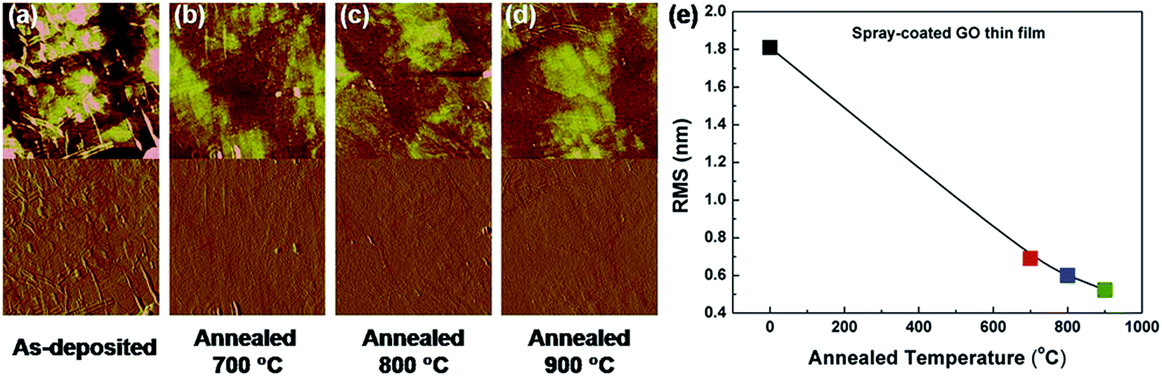 | ||
| Fig. 2 AFM images of (a) as-coated GO layer, and thermally rGO by (b) annealed 700 °C, (c) annealed 800 °C, and (d) annealed 900 °C. (e) The graph of RMS values depend on an annealed temperature of GO. | ||
The chemical compositions of all samples were analyzed by conducting XPS measurements, and the results are shown in ESI, Fig. S1.† XPS results show a C1s peak at 284.8 eV. The C1s spectrum of GO are composed of the five kinds of components that are assigned to C–O or C–OH (hydroxyl, 285.5 eV), C![[double bond, length as m-dash]](https://www.rsc.org/images/entities/char_e001.gif) O (epoxide, 287.2 eV), OC–OH (carboxyl, 288.2 eV), and O–CO (carbonyl, 289.3 eV).33,34 The peak intensity corresponding to the oxygen functional groups in rGO layer gradually decreased with the increase in annealing temperature. The C/O ratio is 0.89 for GO, 2.13 for rGO-700, 2.34 for rGO-800, and 2.71 for rGO-900. It appears that the C/O ratio increases with an increase in annealing temperature, indicating that the oxygen functional groups diminished with thermal annealing. The optical transmittance spectra of GO and rGO layers were shown in ESI, Fig. S2.† We observed that the transmittances of rGO layers are slightly lower than that of GO layer although the thickness of GO layer is higher than that of rGO layers. To further confirm the enhanced electrical property of rGO layers, sheet resistances of rGO-700, rGO-800, and rGO-900 were also measured by a four-point probe technique. The sheet resistances of rGO-700, rGO-800, and rGO-900 are 10.6 × 10³, 6.8 × 10³, and 2.5 × 10³ Ω □−1, respectively. These findings indicate that the sheet resistance of rGO layer decreases with an increase in the C/O ratio. It should be noted that the PCE and short-circuit current (JSC) of the Si-organic solar cell with rGO layer are strongly dependent on both the transmittance and sheet resistance of rGO layers.
O (epoxide, 287.2 eV), OC–OH (carboxyl, 288.2 eV), and O–CO (carbonyl, 289.3 eV).33,34 The peak intensity corresponding to the oxygen functional groups in rGO layer gradually decreased with the increase in annealing temperature. The C/O ratio is 0.89 for GO, 2.13 for rGO-700, 2.34 for rGO-800, and 2.71 for rGO-900. It appears that the C/O ratio increases with an increase in annealing temperature, indicating that the oxygen functional groups diminished with thermal annealing. The optical transmittance spectra of GO and rGO layers were shown in ESI, Fig. S2.† We observed that the transmittances of rGO layers are slightly lower than that of GO layer although the thickness of GO layer is higher than that of rGO layers. To further confirm the enhanced electrical property of rGO layers, sheet resistances of rGO-700, rGO-800, and rGO-900 were also measured by a four-point probe technique. The sheet resistances of rGO-700, rGO-800, and rGO-900 are 10.6 × 10³, 6.8 × 10³, and 2.5 × 10³ Ω □−1, respectively. These findings indicate that the sheet resistance of rGO layer decreases with an increase in the C/O ratio. It should be noted that the PCE and short-circuit current (JSC) of the Si-organic solar cell with rGO layer are strongly dependent on both the transmittance and sheet resistance of rGO layers.
As the wettability of a surface is strongly influenced by its chemical composition, we performed the water contact angle measurements by placing a droplet of DI water on the various rGO surfaces. A 1 μL water droplet was generated using the automatic dispenser of the system. The measurements were performed before and after the GO and rGO layer were stored in air ambient under room temperature for one-month. Fig. 3 shows the water contact angles of GO and rGO-700, rGO-800, and rGO-900 layers. For the surface of the GO layer, we find that the water contact angle is ∼22.06° on the first day and ∼11.72° on the 30th day. The GO layer is expected to have many existing oxygen functional groups attached to the sheet edges, which makes it display hydrophilic properties.35,36 On the other hand, the water contact angle of the rGO layer is about ∼62.3° for rGO-700, ∼66.3° for rGO-800, and ∼71.4° for rGO-900 on the first day. The C/O ratio of the rGO layer increased as the annealing temperature increased. In the results, it is demonstrated that the rGO layer with a high annealing temperature has fewer surface functional groups, resulting in the water contact angle of rGO-900 being larger than that of others. After 30 days, the water contact angle of the rGO layer is about ∼57.9° for rGO-700, ∼62.5° for rGO-800, and ∼67.6° for rGO-900, after one month. The GO layer wettability increased more than the rGO layers after one month. The results show the effectiveness of rGO layer with various annealing temperatures as an anti-corrosion barrier with wetting stability. It implied that rGO layer could act as an oxygen/moisture barrier that can prevent oxygen/water from contacting the Si substrate, results in eliminating surface oxidation at the Si-organic interface.24,29 Consequently, the rGO layer serves as a passivation layer between PEDOT:PSS and Si interface and facilitates enhancement of the lifetime of the Si-organic solar cell.
 | ||
| Fig. 3 (a) The water contact angle of the GO, rGO-700, rGO-800, and rGO-900 layer, respectively. A black body, an oblique line and a check pattern means the measurement dates as initial day, and after 7 and 30 days. (b) The photographs of water drops on the GO, rGO-700, rGO-800, and rGO-900 layer as a function of measurement days. | ||
To investigate the effect of the rGO passivation layer on the Si-organic solar cells performance, our proposed devices were fabricated using PEDOT:PSS as the organic layer and tested under identical conditions. Fig. 4a shows the current density–voltage (J–V) curves of all the devices measured in AM 1.5 illuminated at 100 mW cm−2. The relative short-circuit current (JSC), open-circuit voltage (VOC), fill factor (FF), and PCE of our proposed solar cells are summarized in Table 1. Fig. 4b displays the current–voltage (I–V) curves of our proposed devices, which are PEDOT:PSS/Si solar cells with the GO and rGO layers, measured in dark condition. The PEDOT:PSS/Si without GO layer shows PCE of 5.4%, JSC of 22.3 mA cm−2, VOC of 0.56 V, and FF of 0.49. However, when the GO layer is inserted between PEDOT:PSS and Si, the PCE, JSC, VOC, and FF parameters of solar cell devices are 5.1%, 15.6 mA cm−2, 0.56 V, and 0.59, respectively. We believe that the poor performance is attributable to the many oxygen functional groups of GO. It means that the oxygen functional groups of GO layer (i.e. vacancies and interstitial sites) cause the high charge trap density, resulting in the lower JSC in PEDOT:PSS/Si with GO layer. The PEDOT:PSS/Si devices without and with GO layer exhibit rectification behavior in Fig. 3b. The Schottky barrier formed at the Si-organic interface is responsible for the rectification of major carrier (electron) flows. This property should persist after the insertion of GO passivation layer. The leakage current and saturation current (I0) of the device are lower in a PEDOT:PSS/Si solar cell with an inserted GO layer than that of a PEDOT:PSS/Si solar cell without the GO layer. It is well known that the dark current in a Schottky diode is dominated by majority carrier (electron) injection. Considering that the bandgap of GO increases with the increase of the oxygen functional groups,37 it is possible that the GO layer inserted between the PEDOT:PSS and Si interface blocks the electrons. Then, the electron current is reduced to a point where the hole current starts to dominate the saturation current density, leading to the reduction of leakage current. In addition, we propose that JSC of PEDOT:PSS/Si with GO passivation layer is reduced by the presence of a hole barrier. In other words, in the device with a GO layer, the valence band (EV) of GO could be more aligned with the EV edge of Si, as compared to the PEDOT:PSS/Si without GO layer.2
 | ||
| Fig. 4 (a) The J–V characteristics of Si/PEDOT:PSS solar cells with the inserted GO, rGO-700, rGO-800, and rGO-900 barrier layers, respectively, under illumination of AM 1.5 G, 100 mW cm−2 simulated solar light. (b) A typical I–V characteristics on the logarithmic current scale of corresponding solar cells under dark condition. A estimated energy band diagrams of Si/PEDOT:PSS devices (c) without GO and (d) with GO or rGO barrier layer by annealed 700, 800, and 900 °C. | ||
| Device | JSC (mA/cm2) | VOC (V) | FF | PCE (%) | SBH (eV) |
|---|---|---|---|---|---|
| w/o GO | 22.3 | 0.56 | 0.43 | 5.4 | 0.81 |
| With GO | 15.6 | 0.56 | 0.59 | 5.1 | 0.91 |
| With rGO-700 | 15.6 | 0.44 | 0.60 | 4.1 | 0.74 |
| With rGO-800 | 16.0 | 0.42 | 0.63 | 4.2 | 0.75 |
| With rGO-900 | 12.3 | 0.26 | 0.46 | 1.3 | 0.69 |
For the devices with the inserted rGO passivation layer, the J–V curves show a significant decrease in performance. The JSC, VOC, and PCE of PEDOT:PSS/Si with rGO-700 and rGO-800 layers are 15.6 and 16.0 mA cm−2, 0.44 and 0.42 V, and 4.1 and 4.2%, respectively. The lower JSC and VOC of PEDOT:PSS/Si with rGO-700 and rGO-800 are attributed not only to the high sheet resistance of the rGO layer between PEDOT:PSS and Si but also to the defects in the rGO layer, as compared to a device without the rGO layer. Fig. 4b shows that a rectifying behavior was observed for the PEDOT:PSS/Si with the rGO-700 and rGO-800 layers. The leakage current of PEDOT:PSS/Si device with an rGO-700 and rGO-800 is higher than that of PEDOT:PSS/Si solar cell, which produces a smaller VOC. Considering that the bandgap of the rGO layer decreases with the increase of C/O ratio due to the removal of oxygen functional groups, its electron barrier is lower than that of the GO layer and leads to a higher I0 of the devices with rGO-700 and rGO-800 layers. Besides, we suggest that the EV of rGO-700 and rGO-800 should be higher than that of Si. Hence, the inserted rGO-700 and rGO-800 layers should decrease the JSC of the solar cell compared to the device without the rGO layer. Interestingly, the JSC, VOC, and FF of the PEDOT:PSS/Si solar cell with the rGO-900 passivation layer are 12.3 mA cm−2, 0.26 V, and 1.3%, respectively. The poorer performance of PEDOT:PSS/rGO-900/Si device is a consequence of the ohmic behavior in dark I–V curves, as shown in Fig. 3b. It was noted that the rGO-900 layer should affect electrical properties such as the electron and hole barrier height at the interface between PEDOT:PSS and Si. We proposed that the PEDOT:PSS/Si with rGO-900 passivation layer has a higher reverse current and saturation current (I0) than the others as the rGO-900 layer has a lower band gap and EV caused by higher annealing temperature.
To further verify the decrease in JSC of PEDOT:PSS/Si devices with the inserted GO and rGO passivation layers, the relative parameters (i.e. Schottky barrier height (SBH), work function) were calculated from the corresponding dark I–V curves. The diode characteristics of Schottky junction are described through the thermionic emission theory:38
 | (1) |
 | (2) |
| ΦSBH = WrGO − χSi | (3) |
 | (4) |
Furthermore, the parameter VOC is related to the short-circuit current (ISC), and saturation current (I0). By using eqn (1), the VOC is expressed as:2
 | (5) |
The calculated VOC is estimated as 0.76 eV for PEDOT:PSS/Si without rGO, 0.65 eV for PEDOT:PSS/Si with rGO-700, 0.67 eV for PEDOT:PSS/Si with rGO-800, and 0.58 eV for PEDOT:PSS/Si with rGO-900. These obtained values tend to show similar VOC for all the devices in the J–V curves, as shown in Fig. 3a. As mentioned before, the defects in GO or rGO affect the recombination process of the solar cell.47 The crystalline qualities of GO, rGO-700, rGO-800, and rGO-900 layers determines the defects of GO and rGO layers, and they were examined by Raman spectroscopy. The Raman spectra of the GO, rGO-700, rGO-800, and rGO-900 layers are compared (ESI, Fig. S4†). The Raman spectra of GO consist of two kinds of peaks, which are designated as the G peak (∼1584 cm−1) and the D peak (∼1335 cm−1).48 Peaks for the D and G bands of GO, rGO-700, rGO-800, and rGO-900 layers are clearly resolved (ESI, Fig. S4a†). Peak intensity ratios between the D and G bands, i.e. ID/IG, were calculated (ESI, Fig. S4b†). The ID/IG values for GO, rGO-700, rGO-800, and rGO-900 layers are ∼1.03, 0.79, 0.82, and 0.96, respectively. This indicates an apparent decrease in the ID/IG ratio upon thermal annealing, which suggests that thermal annealing eliminates the oxygen functional groups from GO sheets.49 However, the ID/IG ratio increases when thermal annealing temperature increases to 900 °C. It means that very high temperature leads to further removal of oxygen functional groups, results in high density of disordered carbons in rGO-900 layer.50 Moreover, the ID/IG ratio is related to the average size of in-plane crystallites (La), which corresponds to a mean sp2 GO domain size (or inter-defect distance).51 The La values of GO, rGO-700, rGO-800, and rGO-900 layers are ∼4.31, 5.37, 5.32, and 4.57 nm, respectively. An introduction of a large amount of oxygen functional groups in GO limits the sp2 aromatic size. Thus, the sp2 aromatic size increases with the removal of oxygen functional groups (graphitized) when the samples were annealed at 700 and 800 °C. However, further increase of annealing temperature generates the defects, resulting in the decrease of the sp2 domain size. In other words, the larger inter-defect distance of rGO-700 and rGO-800 tends to enhance the recombination process during the generation and separation of photo-carriers. For this reason, a device with rGO-700 and rGO-800 should have lower leakage current at reverse-bias in dark ambient than a device with rGO-900. As a result, the VOC of solar cells should decrease with the increase in the annealing temperature of the rGO layer, as shown in Fig. 4a. In our proposed devices, we inferred that the rGO layer was optimized by annealing at 700 and 800 °C.
To observe the effect of the hybrid solar cells with GO or rGO passivation layer, the stability of our hybrid solar cells was characterized in air ambient under room temperature. This can be observed from the J–V and I–V characteristics of our proposed devices measured after one-month duration (ESI, Fig. S5 and S6†). Fig. 5a–c show the normalized PCE, JSC, and VOC values over 30 days. As we can see from Fig. 5a, the PEDOT:PSS/Si solar cells with and without GO passivation layers exhibit rapid degradation compared with the others. After 5 days of storage, the PCE of PEDOT:PSS/Si without GO layer reduces by nearly 30% from its initial value. It is contributed by the decrease in JSC of devices and the reduction of VOC of the device in Fig. 5b and c. As some previous reports, the PEDOT:PSS/Si solar cells exhibit poor air stability because organic material is sensitive to oxygen and moisture.9,52,53 As a result, the conductivity of PEDOT:PSS layer dramatically decreases during operation, leading to a sharp decrease of the JSC in solar cells. To confirm the conductivity of PEDOT:PSS layer, Fig. 5d displays the change of series resistance (RS) in solar cells as a function of the time duration. The I–V curve of all devices was also measured in dark condition over 30 days, and the RS of all devices were calculated by:
 | (6) |
 | ||
| Fig. 5 (a) Normalized PCE, (b) JSC, and (c) VOC of Si/PEDOT:PSS solar cell without GO, and with GO, rGO-700, rGO-800, and rGO-900 barrier layer, respectively. (d) The series resistances (RS) of Si/GO or rGO/PEDOT:PSS solar cell as a function of measurement days. | ||
The estimated RS of PEDOT:PSS/Si solar cells increases from ∼5.5 Ω for the first day to ∼700 Ω for 30 days, as shown in Fig. 5d. It is confirmed that the JSC of PEDOT:PSS/Si solar cell decreases with the increase of RS in devices. The VOC of PEDOT:PSS/Si solar cell also decreases with the decline of JSC and the low I0 value as a function of measuring time is given by eqn (5). In addition, the PCE of the PEDOT:PSS/Si with GO passivation layer decreases very fast at the beginning and showed about ∼30% degradation after 3 days. A similar tendency was observed in the increase in RS of PEDOT:PSS/Si with GO passivation layer. These results led to the decrease of JSC and VOC of the PEDOT:PSS/GO/Si device. It appears that the GO layer helps to supply the moisture and oxygen between PEDOT:PSS and Si interface because of higher oxygen functional groups caused by lower C/O ratio, as shown in Fig. 3. By contrast, the PEDOT:PSS/Si with the inserted rGO-700, rGO-800, and rGO-900 passivation layers show a slight degradation in PCE in 31 days. Interestingly, the JSC values of PEDOT:PSS/Si with the rGO passivation layer are stable after one-month, and the VOC values remain at about 90–80% when all devices are kept in air ambient. When the RS of PEDOT:PSS/Si with rGO passivation layer are calculated from the I–V characteristics on dark condition by eqn (6), the obtained values exhibit a marginal variation over 30 days, as shown in Fig. 5d. The RS values of PEDOT:PSS/rGO/Si devices increase by a smaller amount than those of PEDOT:PSS/Si device. This is because of the stable performance of the Si-organic solar cell with the inserted rGO passivation layer.23,25,26 We also confirmed that the surface of rGO layer shows a small variation in the water contact angle as a function of storage time in air ambient, which is depicted in Fig. 3. Considering that the oxygen or moisture diffuse through the PEDOT:PSS layer, the inserted rGO passivation layer prevents the transport of oxygen or moisture on Si substrates, as compared to the GO layer. It can be assumed that the rGO layer helps to interrupt oxidation between PEDOT:PSS and Si interface by oxygen and moisture.29 Moreover, it is possible that the rGO layer can serve as barriers for both liquid and vapor permeants because the typical distance between successive rGO layers is ∼0.3 nm, when the oxygen and moisture pass through the defects in rGO passivation layer stacked between PEDOT:PSS and Si.54–57 Zhang et al. reported that the methyl group termination (–CH3) suppressed the formation of SiOx on Si surface in Si-organic solar cells, and the performance of organic-Si solar cell over time remained unchanged owing to the CH3-termination.58 In this study, the oxidation of Si substrate could be inhibited by use of rGO layer, results in extending lifetime of device with rGO passivation layer. It is well established that the PEDOT:PSS/Si solar cell with rGO layer enhances the air stability of the package-free device as the rGO layer with various annealing temperature play a critical role as a passivation layer in the PEDOT:PSS/Si interface.
4. Conclusions
We investigated the effect of the annealing temperature an rGO layer inserted in PEDOT:PSS/Si hybrid solar cell. The stability of PEDOT:PSS/GO/Si solar cell rapidly deteriorated in air ambient during one-month. The PEDOT:PSS/Si device with rGO-700, 800, and 900 layers shows lower JSC, VOC, and PCE than PEDOT:PSS/Si solar cell without rGO layer. On the other hand, the PCE of PEDOT:PSS/rGO/Si solar cell is more stable than that of PEDOT:PSS/Si device, as observed from the J–V and I–V characteristics in the air during one-month. The JSC values of PEDOT:PSS/rGO/Si solar cell only slightly decreased after one-month, and the RS slightly increased. Additionally, we observed that the rGO layer with high-temperature thermal annealing showed a very small variation in water contact angle over one-month. Consequently, the rGO layer provides not only a surprisingly high level of surface passivation but also prevents corrosion between PEDOT:PSS layer and Si substrate. Our study shows that the thermally annealed rGO layers are suitable as a surface oxidation suppression layers without being packaged, and they provide low-cost production and long-term stability for inorganic–organic hybrid solar cells.Acknowledgements
This research was supported by Basic Science Research Program through the National Research Foundation of Korea (NRF) funded by the Ministry of Education (Grant No. 2013R1A1A2013044 and 2015R1A6A1A04020421).References
- T. Mishima, M. Taguchi, H. Sakata and E. Maruyama, Sol. Energy Mater. Sol. Cells, 2011, 95, 18–21 CrossRef CAS.
- S. Avasthi, S. Lee, Y.-L. Loo and J. C. Sturm, Adv. Mater., 2011, 23, 5762–5766 CrossRef CAS PubMed.
- A. Kumar, S. Sista and Y. Yang, J. Appl. Phys., 2009, 105, 094512 CrossRef.
- J. Schmidt, V. Titova and D. Zielke, Appl. Phys. Lett., 2013, 103, 183901 CrossRef.
- L. He, C. Jiang, H. Wang, D. Lai and Rusli, Appl. Phys. Lett., 2012, 100, 073503 CrossRef.
- W.-R. Wei, M.-L. Tsai, S.-E. Ho, S.-H. Tai, C.-R. Ho, S.-H. Tsai, C.-W. Liu, R.-J. Chung and H. He Jr., Nano Lett., 2013, 13, 3658–3663 CrossRef CAS PubMed.
- F. Zhang, T. Song and B. Sun, Nanotechnology, 2012, 23, 194006 CrossRef PubMed.
- R. Liu, S.-T. Lee and B. Sun, Adv. Mater., 2014, 26, 6007–6012 CrossRef CAS PubMed.
- K. Norman, M. V. Madsen, S. A. Gevorgyan and F. C. Krebs, J. Am. Chem. Soc., 2010, 132, 16883–16892 CrossRef PubMed.
- J. Sheng, K. Fan, D. Wang, C. Han, J. Fang, P. Gao and J. Ye, ACS Appl. Mater. Interfaces, 2014, 6, 16027–16034 CAS.
- J. Chen, E. Cornagliotti, X. Loozen, E. Simoen, J. Vanhellemont, J. Lauwaert, H. Vrielinck and J. Poortmans, J. Appl. Phys., 2011, 110, 126101 CrossRef.
- J. Schmidt, A. Merkle, R. Brendel, B. Hoex, M. C. M. van de Sanden and W. M. M. Kessels, Prog. Photovoltaics, 2008, 16, 461–466 CAS.
- W.-T. Hsu, Z.-S. Tsai, L.-C. Chen, G.-Y. Chen, C.-C. Lin, M.-H. Chen, J.-M. Song and C.-H. Lin, Nanoscale Res. Lett., 2014, 9, 696 CrossRef PubMed.
- Q. Xu, T. Song, W. Cui, Y. Liu, W. Xu, S.-T. Lee and B. Sun, ACS Appl. Mater. Interfaces, 2015, 7, 3272–3279 CAS.
- D. Konios, G. Kakavelakis, C. Petridis, K. Savva, E. Stratakes and E. Kymakis, J. Mater. Chem. A, 2016, 4, 1612–1623 CAS.
- D. Yang, L. Zhou, L. Chen, B. Zhao, J. Zhang and C. Li, Chem. Commun., 2012, 48, 8078–8080 RSC.
- M. M. stylianakis, D. Konios, G. Kakavelakis, G. Charalambidis, E. Stratakis, A. G. Coutsolelos, E. Kymakis and S. H. Anastasiadis, Nanoscale, 2015, 7, 17827–17835 RSC.
- J. Liu, Y. Xue, Y. Gao, D. Yu, M. Durstock and L. Dai, Adv. Mater., 2012, 24, 2228–2233 CrossRef CAS PubMed.
- A. Agresti, S. Pescetelli, L. Cinà, D. Konios, G. Kakavelakis, E. Kymakis and A. D. Carlo, Adv. Funct. Mater., 2016, 26, 2686–2694 CrossRef CAS.
- N. Vaenas, D. Konios, T. Stergiopoulos and E. Kymakis, RSC Adv., 2015, 5, 107771–107776 RSC.
- M. Sygletou, P. Tzourmpakis, C. Petridis, D. Konios, C. Fotakis, E. Kymakis and E. Stratakis, J. Mater. Chem. A, 2016, 4, 1020–1027 CAS.
- D. Konios, C. Petridis, G. Kakavelakis, M. Sygletou, K. Savva, E. Stratakis and E. Kymakis, Adv. Funct. Mater., 2015, 25, 2213–2221 CrossRef CAS.
- X. Liu, H. Kim and L. J. Guo, Org. Electron., 2013, 14, 591–598 CrossRef CAS.
- B. Paci, G. Kakavelakis, A. Generosi, V. R. Alvertini, J. P. Wright, C. Ferrero, D. Konios, E. Strataks and E. Kymakis, RSC Adv., 2015, 5, 106930–106940 RSC.
- J.-M. Yun, J.-S. Yeo, J. Kim, H.-G. Jeong, D.-Y. Kim, Y.-J. Noh, S.-S. Kim, B.-C. Ku and S.-I. Na, Adv. Mater., 2011, 23, 4923–4928 CrossRef CAS PubMed.
- Y.-J. Jeon, J.-M. Yun, D.-Y. Kim, S.-I. Na and S.-S. Kim, Sol. Energy Mater. Sol. Cells, 2012, 105, 96–102 CrossRef CAS.
- H. P. Kim, A. R. B. M. Yusoff and J. Jang, Sol. Energy Mater. Sol. Cells, 2013, 110, 87–93 CrossRef CAS.
- Y.-J. Noh, S.-C. Park, Y.-T. Hwang, J.-H. Choi, S.-S. Kim, C.-H. Jung and S.-I. Na, Carbon, 2014, 79, 321–329 CrossRef CAS.
- X. Gao, J. Jang and S. Nagase, J. Phys. Chem. C, 2010, 114, 832–842 CAS.
- W. S. Hummers Jr. and R. E. Offemen, J. Am. Chem. Soc., 1958, 80, 1339 CrossRef.
- S. Jeong, E. Garnett, S. Wang, Z. Yu, S. Fan, M. Brongersma, M. McGehee and Y. Cui, Nano Lett., 2012, 12, 2971–2976 CrossRef CAS PubMed.
- J.-H. Hyung, G.-S. Kim, J.-T. Jeong, I.-H. Choi, C.-H. Hong, S. Yun, J.-H. Koh and S.-K. Lee, J. Nanoelectron. Optoelectron., 2015, 10, 229–233 CrossRef CAS.
- A. Misra, H. Kalira and A. Kottantharayil, ACS Appl. Mater. Interfaces, 2014, 6, 786–794 CAS.
- B. D. Ryu, J.-H. Hyung, M. Han, K. B. Ko, Y. J. Park, T. V. Cuong, J. Cho and C.-H. Hong, Mater. Sci. Semicond. Process., 2016, 44, 1–7 CrossRef CAS.
- J. Rafiee, M. A. Rafiee, Z.-Z. Yu and N. Koratkar, Adv. Mater., 2010, 22, 2151–2154 CrossRef CAS PubMed.
- G.-T. Kim, S.-J. Gim, S.-M. Cho, N. Koratkar and I.-K. Oh, Adv. Mater., 2014, 26, 5166–5172 CrossRef CAS PubMed.
- M. Acik and Y. J. Chabal, J. Mater. Sci. Res., 2013, 2, 101–112 CAS.
- Metal–semiconductor contacts, in Physics of Semi-conductor Devices, ed. S. M. Sze and K. K. Ng, John Wiley & Sons, Hoboken, 3rd edn, 2007 Search PubMed.
- X. Li, H. Zhu, K. Wang, A. Cao, J. Wei, C. Li, Y. Jia, Z. Li, X. Li and D. Wu, Adv. Mater., 2010, 22, 2743–2748 CrossRef CAS PubMed.
- E. Shi, H. Li, L. Yang, L. Zhang, Z. Li, P. Li, Y. Shang, S. Wu, X. Li, J. Wei, K. Wang, H. Zhu, D. Wu, Y. Fang and A. Cao, Nano Lett., 2013, 13, 1776–1781 CAS.
- A. M. Nardes, M. Kemerink, M. M. De Kok, E. Binken, K. Maturova and R. A. J. Janssen, Org. Electron., 2008, 9, 727–734 CrossRef CAS.
- N. T. Khoa, S. W. Kim, D.-H. Yoo, E. J. Kim and S. H. Hahn, Appl. Catal., A, 2014, 469, 159–164 CrossRef CAS.
- J. Liu, M. Curstock and L. Dai, Energy Environ. Sci., 2014, 7, 1297–1306 CAS.
- S.-S. Li, K.-H. Tu, C.-C. Lin, C.-W. Chen and M. Chhowalla, ACS Nano, 2010, 4, 3169–3174 CrossRef CAS PubMed.
- R. Garg, N. K. Kutta and N. R. Choudhury, Nanomaterials, 2014, 4, 267–300 CrossRef.
- K. W. Kim, W. Song, M. W. Jung, M.-A. Kang, S. Y. Kwon, S. Myung, J. Lim, S. S. Lee and K.-S. An, Carbon, 2015, 82, 96–102 CrossRef CAS.
- M. Zhu, X. Li, Y. Guo, X. Li, P. Sun, X. Zang, K. Wang, M. Zhong, D. Wu and H. Zhu, Nanoscale, 2014, 6, 4909–4914 RSC.
- A. C. Ferrari, Solid State Commun., 2007, 143, 47–57 CrossRef CAS.
- Z. Wang, D. Xu, Y. Huang, Z. Wu, L. Wang and X. Zhang, Chem. Commun., 2012, 48, 976–978 RSC.
- Thermal reduction of graphene oxide, in Physics and Applications of Graphene-Experiments, Nanotechnology and Nanomaterials, ed. S. Mikhailov, 2011 Search PubMed.
- L. G. Cançado, K. Takai, T. Enoki, M. Endo, Y. A. Kim, H. Mizusaki, A. Jorio, L. N. Coelho, R. Magalhães-Paniago and M. A. Pimenta, Appl. Phys. Lett., 2006, 88, 163106 CrossRef.
- M. G. Walter, X. Liu, L. E. O'Leary, B. S. Brunschwing and N. S. Lewis, J. Phys. Chem. C, 2013, 117, 14485–14492 CAS.
- A. Guerrero, P. P. Boix, L. F. Marchesi, T. R.-Sanchis, E. C. Pereira and G. G.-Belmonte, Sol. Energy Mater. Sol. Cells, 2012, 100, 185–191 CrossRef CAS.
- O. C. Compton, S. Kim, C. Pierre, J. M. Torkelson and S. T. Nguyen, Adv. Mater., 2010, 22, 4759–4763 CrossRef CAS PubMed.
- R. R. Nair, H. A. Wu, P. N. Jayaram, I. V. Grigorieva and A. K. Geim, Science, 2012, 335, 442–444 CrossRef CAS PubMed.
- F. Guo, G. Silverberg, S. Bowers, S.-P. Kim, D. Datta, V. Shenoy and R. H. Hurt, Environ. Sci. Technol., 2012, 46, 7717–7724 CrossRef CAS PubMed.
- Z. Liu, J. Li and F. Yan, Adv. Mater., 2013, 25, 4296–4301 CrossRef CAS PubMed.
- F. Zhang, B. Sun, T. Song, X. Zhu and S. Lee, Chem. Mater., 2011, 23, 2084–2090 CrossRef CAS.
Footnotes |
| † Electronic supplementary information (ESI) available. See DOI: 10.1039/c6ra12441k |
| ‡ B. D. Ryu and J.-H. Hyung contributed equally in this work. |
| This journal is © The Royal Society of Chemistry 2016 |