
Recent advances in non-chemically amplified photoresists for next generation IC technology
Subrata Ghosh
*a,
Chullikkattil P. Pradeep
*a,
Satinder K. Sharma
b,
Pulikanti Guruprasad Reddy
a,
Satyendra P. Pal
a and
Kenneth E. Gonsalves
*a
aSchool of Basic Sciences, Indian Institute of Technology Mandi, Himachal Pradesh – 175005, India. E-mail: subrata@iitmandi.ac.in; pradeep@iitmandi.ac.in; kenneth@iitmandi.ac.in
bSchool of Computing and Electrical Engineering, Indian Institute of Technology Mandi, Himachal Pradesh – 175005, India
First published on 20th July 2016
Abstract
While chemically amplified resists (CARs) have been dominating the semiconductor industries over the past few decades, particularly in the area of computer chip fabrication, the replacement of such resists has been realized in recent times as the CARs are approaching their resolution limit, and thus may not be able to fulfil the market demand that the semiconductor industries are looking for, particularly for sub-20 nm node technology using next generation lithography techniques. In this context, non-chemically amplified resists (n-CARs) are being anticipated as potential replacements of CARs. In the case of n-CARs, the photosensitive functionality is integrated into the resist backbone. Therefore, upon exposure to photons of suitable energy, the photosensitive group undergoes photochemical changes resulting in polarity switching between the exposed and unexposed regions. This polarity change helps in developing patterns in the presence of a suitable developer. Therefore, external chemical amplification using photoacid generators (PAGs) is not needed to bring in required polarity changes in the case of n-CARs. As the n-CARs do not require any additional chemical amplification, they are devoid of the most serious problem that almost all CARs face i.e. acid diffusion in the solid state causing considerable line-edge roughness (LER) and line-width roughness (LWR). Recently, several research groups have designed and developed various n-CARs with ultra-low resolution and LER/LWR. Although many n-CARs, sensitive to photons of various energies, have been developed over the last few decades for larger nodes (>60 nm) the n-CARs development for patterning sub-30 nm features is at the plinth level. This review article will focus on the recent developments in the area of n-CARs for sub-30 nm node technology using next generation lithography (NGL) techniques.
 Subrata Ghosh | Subrata Ghosh received his PhD in Organic Chemistry from IIT Guwahati followed by postdoctoral studies at Bar-Ilan University (Israel), Case Western Reserve University (US) and University of Leipzig (Germany). He is the recipient of the Alexander von Humboldt Fellowship. Currently he is working as Associate Professor at IIT Mandi. His research interests include organic soft materials, organic emissive dyes for bioimaging, organic light emitting diodes (OLEDs), high energetic materials, polymer chemistry, chemical sensors and photoresists for micro/nanoelectronics. |
 Chullikkattil P. Pradeep | Chullikkattil P. Pradeep received Ph.D in Inorganic Chemistry from University of Hyderabad, India in 2006. After Ph.D, he received the International Incoming Fellowship from Royal Society to do post-doctoral studies with Professor Leroy Cronin at University of Glasgow, where he worked on organic–inorganic hybrids till 2010. He joined the School of Basic Sciences, Indian Institute of Technology Mandi in 2010, where he is an Associate Professor currently. His research interests include hybrid photoresists for high resolution nano-lithography, polyoxometalate chemistry, photo-responsive materials, fluorescent sensors and coordination complexes. |
 Satinder K. Sharma | Satinder K. Sharma received the Master of Science in Physics (Electronic Science) from Himachal Pradesh University, Shimla, India, in 2002 and the Ph.D. degree from Department of Electronic Science, Kurukshetra University, Kurukshetra, India, in 2007. From 2007 to 2010, he was a Postdoctoral Fellow at the DST Unit on Nanosciences, Dept. CHE, Indian Institute of Technology (IIT) Kanpur, Kanpur, India. From 2010 to 2012 he worked as faculty in the Electronics and Microelectronics Division, Indian Institute of Information Technology (IIIT), Allahabad, India. From 2012 onwards, he has been working as faculty in the School of Computing and Electrical Engineering (SCEE), at Indian Institute of Technology (IIT), Mandi, (Himachal Pradesh), India. His current research interests include micro & nano electronics circuits design, polymer nanocomposite, sensors, photovoltaic and self-assembly. |
 Pulikanti Guruprasad Reddy | Pulikanti Guruprasad Reddy received Master of Science degree in Chemistry from Sri Krishnadevaraya University, Anathapur, A.P, in 2011. He then joined in Ph.D program under the guidance of Dr. Pradeep C. Parameswaran in School of Basic Science, Indian Institute of Technology (IIT) Mandi, H.P, India in 2013. Currently, he is working as senior research fellow with Prof. Kenneth E. Gonsalves and his interdisciplinary team for the development of next generation integrated circuits (IC) at sub-20 nm nodes. His research interest includes polyoxometalates, crystallography, self-assembly, organic–inorganic hybrids, lithography, device fabrication and catalysis. |
 Satyendra P. Pal | Satyendra Prakash Pal received his PhD from Jawaharlal Nehru University, New Delhi, India, in 2014. He has two years postdoctoral experience in nanodevice fabrications and their ultralow temperature study at Indian Institute of Science Education and Research Mohali, Punjab, India. Presently he is working as a postdoctoral fellow at the Indian Institute of Technology (IIT) Mandi, Himachal Pradesh, India. He is working on the next generation lithography techniques for the nanopatterning of the nonchemically amplified resists at sub-20 nm half pitch. |
 Kenneth E. Gonsalves | Since Jan 2012 Dr Gonsalves is Distinguished Professor at IIT Mandi. Prior to that Prof. Gonsalves was the Celanese Acetate Distinguished Professor at the University of North Carolina at Charlotte (UNCC) from 2001 to 2014. He was also a faculty member at the Center for Optoelectronics and Optical Communications at UNCC. His research has been focused on materials synthesis: organic polymer chemistry, organometallic polymers, polymer and molecular precursors for ceramics and intermetallics; nanostructured materials/composites; biomaterials; novel resists for nanolithography; nanofabrication and nanopatterning of biomaterials; organic and hybrid nanomaterials for energy harvesting, nanoscale drug delivery devices. His recent projects on nanolithography have been supported by the US NSF, DARPA, SEMATECH INT, INTEL Corp. & Rohm and Haas/Dow Electronic Materials. |
1. Introduction
Since the invention of computers, efforts have been directed towards miniaturization of devices through development of advanced materials and technologies to make the final electronic devices as small as possible. The development of an integrated circuit (IC) has made it possible to make portable computers with faster processing times.1 Now there is a race against time to make the processing time even quicker. This requires making the nanopatterns in the ICs much smaller. The manufacturing of ICs typically includes a lithography process (Fig. 1). The key ingredient for an efficient photolithography process is the photoresist which in fact helps in controlling ultimate feature sizes on silicon wafers.2–7 These photoresists are the molecular or macromolecular chemical entities. They could be pure organic or organic–inorganic hybrid or organometallic or pure inorganic systems with high photosensitivity.7–24 Depending upon their solubility in developer solution after exposure to suitable radiation, the resists have been classified into two categories, viz. positive and negative tone resists. Upon irradiation of the resist materials with the light of suitable wavelength, if the portion which is exposed to the radiation becomes insoluble in developer solution, then the resist is called a negative tone photoresist. However, if the exposed region becomes soluble in developer, then the resist is called a positive tone resist (Fig. 1).9–34 Researchers have developed several positive and negative photoresist materials over the last few decades for semiconductor industries.9–34 Whereas the current market size of these materials is $3.2 Bn, the projected market size by 2020 is ∼$5 Bn. Till date, CARs have been dominating the semiconductor industries, and have been proven to be the only class of materials with high potential in patterning nanofeatures in ICs.35–41 But, it is now being anticipated that these CARs will fail to meet the market demand as they are approaching their resolution limit particularly for sub-20 nm technologies.12,42–44 Given the huge market demand of semiconductor industries, and considering that the CARs are approaching their limits for patterning sub-20 nm features for ultrasensitive IC chips for nanoelectronics, n-CARs are expected to fulfil the market demand with their potential in patterning sub-20 nm features with low line edge and line width roughness (LER/LWR).9–24 The tangible development on new n-CARs for sub-30 nm nodes has happened only in the last few years. These n-CARs are either molecular or macromolecular (polymeric) chemical entities.7–24 With these molecular and macromolecular resists, sub-20 nm patterning has already been achieved with very low LER and LWR. There are many key parameters that need to be improved in order to address some issues currently facing by academic as well as semiconductor industry community. As the actual development is very fresh, and as it is expected that n-CARs are going to replace current resist workhorses, this field has enormous importance, both fundamental and commercial.9–34 For CARs, the contest between sensitivity, resolution and LWR has been called the ‘triangle of death’ for sub-20 nm technology (Fig. 2).12,45,46 Although the aim of every researcher has been to develop unique resists which possess all these three properties simultaneously i.e. high sensitivity, excellent resolution and good LWR, majority of the resists reported so far have compromised with at least one of these properties even though other two have been achieved successfully. This has been presented graphically in Fig. 2 indicating that the trade-off among these parameters has been the major concern in the area of photoresists development and efforts are being directed to eliminate these trade-offs with the development of highly efficient resists. As these problems are mainly associated with chemically amplified positive tone resist materials, in recent times, attention has focused on the development of n-CARs for future lithography nodes.9–34 | ||
| Fig. 1 General schematic representation of lithographic imaging process. | ||
 | ||
| Fig. 2 Schematic on the most common trade-off between the critical parameters for sub-20 nm lithography technology. | ||
As the development of n-CARs for sub-30 nm nodes is in the plinth level, this article will help in understanding the scientific and commercial importance of these chemical systems. The fundamentals as well as advanced information on recent development will also help to design new resists with much better performance to meet the market demand (projected in the International Technology Roadmap for Semiconductor Industries, ITRS-2015).47
2. Non-chemically amplified photoresists (n-CARs)
The n-CARs stand different from the CARs mainly at the mode of polarity switching upon exposure. While for CARs the difference in polarity of the exposed area from that of unexposed area is brought out by exposing the resist films either by radiation or by light in the presence of externally added photoacid generators (PAGs), for n-CARs, the PAGs or the photosensitive units are embedded into the resists architecture, and hence external chemical amplification is not needed.12–24,48 As the polarity switching is done internally without any need for external chemical amplification, the resist formulations for n-CARs are much simpler as compared to CARs.In the last few years, wide ranging n-CARs have been developed with varying sensitivity for patterning smaller features (30 nm or beyond) with high degree of resolution. Depending on their chemical composition and mode of patterning, the following are the most common and efficient n-CARs.
2.1 Non-chemically amplified organic photoresists (n-CAORs)
The n-CAORs typically contain light/radiation sensitive functionality in their chemical architecture which eventually undergoes photo-degradation when exposed to either radiation (for example, electron beam) or suitable energy light. This radiation or light mediated solid phase chemical modification ultimately results in polarity change in the exposed region as compared to unexposed region. So far, these n-CARs have been reported to be either of polymeric nature or of dendritic nature with relatively higher molecular weight. Efforts have been directed to improve the sensitivity, resolution, LER/LWR of the base-resists through chemical structure modifications. The recently developed n-CAORs are categorized and described below.The following sub-sections will discuss recent developments in the area of positive tone n-CARs, particularly for lower nodes.
2.1.1.1 Non-chemically amplified positive tone polymeric photoresist. As it has been evaluated and reported that the diffusive path-length of the protons or counterions generated by the PAGs during exposure of CARs is in the range of 11–25 nm, such diffusion becomes detrimental to patterned features as the diffusion path length is a significant distance when compared with the target dimensions of the features (20 nm or beyond) patterned by EUV lithography.58–60 Whittaker and co-workers recently reported an innovative highly sensitive (4–6 mJ cm−2) positive tone chain scission organic n-CAR platform with comb architecture (Fig. 3) for patterning 30 nm or beyond features (Fig. 4).60 The developed resists bear photosensitive sulfone functionality which undergoes photodegradation upon exposure with EUV photons, and brings in polarity difference between exposed and unexposed areas.
 | ||
| Fig. 3 Chemical structure of the sulfone based non-chemically amplified positive resist.60 | ||
 | ||
Fig. 4 AFM height images of 1![[thin space (1/6-em)]](https://www.rsc.org/images/entities/char_2009.gif) :1 line-space patterns showing at resolutions of 50 nm, 30 nm and 22.5 nm half-pitch. The corresponding critical dimensions (CD), LER and dose to resist are shown on the images. Reproduced from ref. 60 with permission from the Royal Society of Chemistry. :1 line-space patterns showing at resolutions of 50 nm, 30 nm and 22.5 nm half-pitch. The corresponding critical dimensions (CD), LER and dose to resist are shown on the images. Reproduced from ref. 60 with permission from the Royal Society of Chemistry. | ||
Their design combines poly(olefin sulfone) backbone with poly(methyl methacrylate) (PMMA) arms in order to increase structural stability. Upon EUV exposure, the resist underwent fast photodegradation with very high sensitivity. A mixture of isopropyl alcohol and methylisobutylketone was used as developer while patterning the silicon surface with the developed resists. They preformed head space mass spectrometry studies to get insight into the degradation behavior of the of resist materials under EUV irradiation. It was observed that the poly(olefin sulfone) backbone undergoes preferential photodegradation followed by depolymerization when irradiated under vacuum conditions.
These experimental outcomes were further supported by the grazing-angle total attenuated reflectance FT-IR (GATR-FT-IR) spectroscopy which indicated that the peaks corresponding to PMMA remained unchanged after irradiation with EUV photons while those corresponding to the poly(olefin sulfone) backbone decreased. All these experimental results reveal that the incorporation of sulfone functionality, as potential photodegradable unit, into polymer backbone while designing new photoresists for NGL might result highly sensitive materials. Eventually, a large number of n-CARs have been developed through incorporation of sulfone functionality into polymer backbone.61,62 Later, the same group reported another interesting aqueous developable positive tone resist platform which follows a combined switching mechanism that includes both polarity change as well as molecular weight change upon exposure with photons and electron-beams (Fig. 5).63 In general, the conventional photoresists rely on a single switching mechanism which could be either a change in polarity or, molecular weight of the polymer. In order to induce polarity change upon exposure with radiation or light, photosensitive o-nitrobenzyl ester functionality was introduced into polymer backbone as pendant group. Upon interaction with photons, the hydrophobic ester functionality undergoes photochemical cleavage resulting in the formation of hydrophilic carboxylic acid groups and thus brings in changes in polarity. Whereas, the molecular weight switch was achieved by introducing poly(olefin sulfone) into polymer backbone which eventually undergoes photo-induced chain scission (Scheme 1). The 193 nm interference lithography and electron-beam lithography techniques were utilized to assess the patterning potential as well as to determine the sensitivity of these resist systems. The photodeprotection of nitrobenzyl group was investigated by analyzing the GATR-FT-IR spectra of light exposed thin film of these polymers. The same technique was used to study the chain scission. Resolution of approximately 32 nm was achieved using e-beam lithography (Fig. 6). It was also investigated in detail how the post exposure bake (PEB) temperature affects LER of the developed patterns.
 | ||
| Fig. 5 Aqueous developable dual switching sulfone based positive photoresists for 193 nm interference and electron-beam lithography.63 | ||
 | ||
| Scheme 1 Schematic diagram of a poly(olefin sulfone)-based photoresist that functions through both molecular weight and polarity solubility switch.63 | ||
 | ||
| Fig. 6 Top-down SEM micrographs of approximately 32 nm trenches patterned in polymer B1. This figure has been reproduced from ref. 63 with permission from Wiley Online Library. | ||
Given that the incorporation of suitable photosensitive functionality into polymer backbone leads to desired polarity change through solid state photochemical reaction upon interaction with radiation or photons of suitable energy, it was proved experimentally through the development of suitable resist platform that the introduction of aliphatic tertiary carbonates into polymer backbone may result in highly sensitive chain scission positive tone photoresists for EUV lithography (Fig. 7).64 These polycarbonates were successfully used to pattern nanofeatures with critical dimension (CD) 28.6 nm. The polarity switching of these resists is mainly due to molecular-weight switch when they interact with light.
 | ||
| Fig. 7 Polycarbonates for EUVL. This figure has been reproduced from ref. 64 with permission from Wiley Online Library. | ||
The very well-known resist, poly(methylmethacrylate) (PMMA), has been used extensively as non-chemically amplified positive tone chain scission resist for patterning nanofeatures using e-beam, liquid immersion interference and EUV lithography.65–69 Flanders reported the potential of PMMA in patterning 17.5 nm features with line/space characteristics using carbon K X-rays (λ = 4.5 nm) with the help of a proximity technique.65 The same resist was successfully used for printing 19 nm line/space patterns using EUV lithography.66 Although PMMA is known as e-beam resist, Bloomstein et al. reported 27 nm line/space printing with PMMA using liquid immersion interference lithography at 157 nm as patterning tool.67 Interestingly, PMMA has been used to pattern features as low as 4 isolated lines using e-beam lithography (Fig. 8).68 Such low size nanopatterns were developed using a ultrasonically-assisted development process where a mixture of water and isopropyl alcohol was used as developer. Hence, PMMA is one of the most widely used n-CARs which shows sensitivity toward many NGL techniques.
 | ||
| Fig. 8 SEM image of 4 nm lines patterned by PMMA using e-beam lithography. This figure has been reproduced from ref. 68 with permission from American Institute of Physics. | ||
2.1.1.2 Non-chemically amplified positive tone molecular photoresist. The lithography and associated techniques have been proven to be the key technology for fabricating smart devices for nanoelectronics.7,36–39,47 In this regard, photoresists have been the core materials to print electronic circuits on silicon substrates. Majority of the exiting resists materials are based on polymers largely because of their several advantages that include amorphous character, flexibility and processability.70–73 But their disadvantage is their large molecular size which eventually affects line-edge roughness of the developed patterns particularly for sub-20 nm node technology. To overcome this issue, many research groups started developing molecular resists with much smaller size. As the polymer molecules are typically of the size of 3–5 nm, each sub-20 nm node width will correspond to 5–6 polymer molecules. Hence, the resolution and LER in the case of polymer resists are predicted to be inferior as compared to those of molecular resists largely because of their larger size (Fig. 9).25 In addition to these, it is expected that the molecular resists will not suffer from intermolecular chain entanglement like polymers which eventually can lead to internal stress or swelling, and hence the patterns distortion can be avoided in larger extent. Moreover, one can expect smooth homogenous thin film formation onto suitable lithography substrate as the molecular resists are composed of identical molecules. One has to remember that the molecular resist materials should be amorphous in nature so that it does not crystallize on the time scale of use and should form uniform amorphous film during lithography process. Though large number of chemically amplified molecular resists have been developed over the years,25–28 non-chemically amplified molecular resists are small in number.
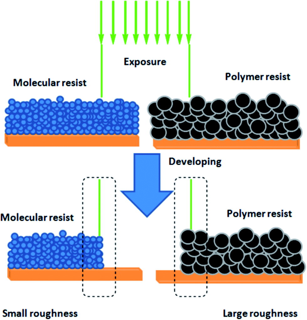 | ||
| Fig. 9 Schematic diagram of patterning properties of molecular resist and polymer resist.25 | ||
Henderson and co-workers reported new class of two molecular positive tone n-CARs for DUV lithography (Fig. 10).29 These resists were developed by introducing 2-nitrobenzyl functionality as photosensitive protecting group into molecular architecture. The photo-mediated deprotection of this functionality ultimately converts the dissolution inhibiting chemical entity into a dissolution promoter, and hence the exposed areas get dissolved in a polar developer making these resists as positive tone molecular resists. Whereas, one resist was developed based on deoxycholic acid (NBnDch), the other one was on aromatic platform bearing two phenolic groups (NBnHPF). The NBnHPF was found to be more sensitive to DUV photons than NBnDch. The most important development was a unique resist formulation with a calixarene dissolution promoter which exhibited extremely low dose-to-clear value of only 1 mJ cm−2. It is worth mentioning that despite of their excellent DUV sensitivity, they were found not to possess high sensitivity when exposed using extreme ultraviolet or e-beam exposure sources.
 | ||
| Fig. 10 Chemical structures of positive tone molecular n-CARs for DUVL.29 | ||
Ito et al. reported o-nitrobenzyl phenol ether (NBP) based non-chemically amplified positive-tone molecular photoresist which possesses potential for printing half-pitch (hp) 32 nm line and space (L/S) patterns with lower line edge roughness (LER) when patterning was done using near-field lithography.30 Although the sensitivity of this resist was not very high in terms of the dose required for patterning, NBP was successfully used to print 22 nm L/S features with 10 nm depths.
Hence, the development of negative tone resists is highly essential for specialized applications. Though a large number of positive resists are available in the literature,25–33 the number of negative resists is relatively less.9–11,34 The following sub-sections will deal with the recent development on negative tone n-CARs.
2.1.2.1 Non-chemically amplified negative tone polymeric photoresist. As the aqueous developable resists77 with patterning potential for sub-20 nm features are more desirable, recently the possibility of using well known photosensitive functionality, triflate ion, as light/radiation mediated polarity modulator was explored extensively. Its incorporation into resists architecture led to the formation of ionic highly polar negative tone n-CARs. In this endeavor, a library of sulfonium based non-chemically amplified negative tone photoresists with varying polymer microstructures for e-beam and EUV lithography was successfully developed (Fig. 11).12–18 It has been shown that some of these polymeric resists materials can pattern 20 nm 1
:1 line:space features (Fig. 12) with ultralow LER that varies from 1.8 ± 0.3 to 2.3 ± 0.4 nm.12,13 The polymer microstructures have been found to play an important role in improving the sensitivity as well as resolution potential.12–14 For example, the polymerization of (4-(methacryloyloxy)phenyl)dimethylsulfoniumtriflate (MAPDST) led to the development of poly(MAPDST) homopolymer which was found to be sensitive to e-beam radiation as well as extreme ultraviolet (EUV) photons, and to have potential in patterning 20 nm L/S features with very low LER/LWR.14 The sensitivity was calculated to be ∼90 mJ cm−2. The incorporation of methylmethacrylate unit into polyMAPDST backbone as dissolution inhibitor led to the development of a copolymer, poly(MAPDST-co-MMA), with much improved sensitivity (Fig. 11). These resists were investigated to have very high etch resistance with respect to silicon substrate. The etch resistance was much higher than many commercial resists. As the thermal stability is an important parameter for any photoresist to be used for lithography applications, we have successfully shown that the inclusion of ferrocene functionality into polymer backbone as pendant organometallic unit leads to better thermal stability with improved sensitivity of the resulting copolymer, MAPDST–FMMA as compared to the polyMAPDST.19
 | ||
| Fig. 11 Chemical structures of negative tone polymeric n-CARs.12,14,78 | ||
 | ||
| Fig. 12 (a) AFM surface topography image of 2.4 × 2.4 μm area for non-chemically amplified MAPDST–MMA copolymer resist. (b) 3D images of MAPDST copolymer resist patterns with the regular space 25 nm (left) and 20 nm (right path). (c) The depth profile analysis and section investigation. Adapted with permission. Copyright 2014 SPIE Journals.13 | ||
To understand in depth with experimental evidences the photo degradation of these negative tone resists upon exposure with EUV photons, the resists were exposed with synchrotron radiation (SR) at the Brazilian Synchrotron Light Source (LNLS), Campinas, Brazil. The XPS spectroscopy was used to prove the surface chemical changes of poly MAPDST thin film after irradiation. The changes in the surface chemistry with the irradiation time can be seen clearly in the HR-XPS spectra of C 1s envelope (Fig. 13).14 The C 1s HR-XPS spectra revealed clear change in the surface chemistry of the poly MAPDST film upon irradiation at 103.5 eV. Whereas, the untreated films showed typical signals corresponding to the aliphatic and aromatic contributions (C–C/C–H), C–O, COO and CF3 functionalities, after one minute of irradiation the CF3 and COO contributions in the XPS spectra almost disappeared. Also, the C–O contribution was strongly affected by the SR light. The CF3 (from triflate) and the ester groups seemed to be the weakest parts in the poly MAPDST composition.
 | ||
| Fig. 13 High-resolution XPS spectra of the C 1s envelope of the MAPDST homopolymer films before irradiation and after 1 and 5 min of SR irradiation at 103.5 eV. Adapted with permission. Copyright 2015 American Chemical Society.14 | ||
The complex nanofeatures are gaining utmost interest in the area of high-density magnetic recording, photonic crystals, information storage, micro-lens arrays, tissue engineering, and catalysis. Photoresists are used extensively to develop wide ranging complex nano-features. Very recently, we reported the potential of poly MAPDST in patterning highly ordered complex nano-features that include nanodots, nanowaves, nanoboats, nanopillar and star-elbow features (Fig. 14, 15 and 16 (A & C)) using EUV lithography. Some of these features i.e., nanopillars and star-elbow features were further characterized by atomic force microscopy (Fig. 16(B & D)).15 The AFM images revealed that the patterns were fully developed up to the silicon surface. We also have shown successful pattern transfer by adapting compatible etch recipes into silicon substrate using polyMAPDST.15
 | ||
| Fig. 14 (A) FE-SEM images of highly dense arrays of 60, 50, 45, 40, 36 and 34 nm dots; (B) higher magnification (60k) images of nanodots (EUV dose 88.19 mJ cm−2). Adapted with permission. Copyright 2016 Nature publishing group.15 | ||
 | ||
| Fig. 15 (A) FE-SEM images of EUV exposed nanowaves and nanoboats; (B) higher magnification images (magnification: 120k) of nanowaves; (C) higher magnification images (magnification: 120k) of nanowaves and nanoboats (EUV dose 88.19 mJ cm−2). Adapted with permission. Copyright 2016 Nature Publishing Group.15 | ||
 | ||
| Fig. 16 (A) FE-SEM images of EUV exposed nanopillars; (B) 3-D view of AFM images of nanopillars; (C) FE-SEM images of star-elbow features; (D) 3-D view of AFM images of star-elbow features (EUV dose 88.19 mJ cm−2). Adapted with permission. Copyright 2016 Nature Publishing Group.15 | ||
Barrios and co-workers reported recently an innovative resist platform, poly(2-hydroxyethyl methacrylate-co-2-methacrylamidoethyl methacrylate) (P(HEMA-co-MAAEMA)) (Fig. 17), for e-beam lithography with ultrahigh sensitivity (0.5 μC cm−2) and a low contrast of 1.2.79 The sensitivity of this novel system was calculated to be one order of magnitude less than those of many commercially available CARs. All these exciting properties make this resist system ideal for creating organic and inorganic 3D micro–nano-structures. XPS measurements were performed to understand in depth the structural changes that happened upon electron irradiation (Fig. 18). Thorough characterization revealed the formation of new bonds and no change in chemical composition upon electron exposure. As etch resistance of any new resist is an important parameter, this resist showed remarkable adherence to silicon substrates without the assistance of adhesion promoters or thermal treatments and, high resistance to both dry as well wet etching with respect to silicon. Interestingly, varying exposure doses tuned the chemical reactivity of this copolymer composition, and hence the same resist was successfully used as negative as well as positive tone resist.
 | ||
| Fig. 17 Chemical structure of poly(HEMA-co-MAAEMA).79 | ||
 | ||
| Fig. 18 XPS [C 1s (left) and O 1s (right)] spectra of an unexposed P(HEMA-co-MAAEMA) film and an irradiated (dose 1/4 10 mC cm−2) poly(HEMA-co-MAAEMA) area. Reproduced from ref. 79 with permission from the Royal Society of Chemistry. | ||
As they are known for their sensitivity toward electron-beams, ZEP brand resists have also been used extensively as both positive and negative tone resists for printing sub 30 nm nodes by tuning the developing conditions.80–83 Using a suitable developer, the sensitivity of ZEP-520A has been achieved as low as 2.6 μC cm−2.
2.1.2.2 Non-chemically amplified negative tone molecular photoresist. The importance as well as the need of molecular resists has been described in one of the previous sections. Similar to positive tone molecular n-CAR, only few negative tone molecular n-CARs have been successfully developed and reported in the literature.
Given that the resist materials with potential in patterning less than 10 nm features are expected to be useful for quantum device applications, Fujita and co-workers reported utilization of a calixarene derivative, hexaacetate p-methnylcalix[6]arene (MC6AOAc) (Fig. 19(a)), as a negative tone n-CAR for electron-beam lithography.9 They successfully patterned sub-10 nm features on Ge substrate with little side roughness (Fig. 20(a)). Interestingly, the resist showed high durability to halide plasma etching which allowed efficient pattern transfer to Ge resulting in the fabrication of almost defect free 7 nm nanowires (Fig. 20(b)). The sensitivity of MC6AOAc was evaluated to be 20 nC cm−2 with a beam current of 100 pA at 30 kV acceleration voltage. Also, being a molecular resist with molecular weight 972, its monodispersity helped in forming very smooth film with surface roughness less than 2 nm.
 | ||
| Fig. 19 Chemical structure of (a) MC6AOAc and, (b) CMC6AOMe.11 | ||
 | ||
| Fig. 20 Pattern transfer to Ge, (a) SEM image of resist pattern on Ge, and (b) SEM image of transferred Ge pattern. This figure has been reproduced from ref. 9 with permission from American Institute of Physics. | ||
Later, in addition to MC6AOAc, Fujita group showed the utilization of another negative tone molecular n-CAR, 5,11,17,23,19,35-hexachloromethyl-37,38,39,40,41,42-hexa-methoxycalix[6]arene (CMC6AOMe) (Fig. 19(b)) for nanopatterning using electron-beam lithography.11 Both the resists were established to be high-resolution negative resists with potential in patterning highly dense arrays of dots of 12 nm diameter with 25 nm pitch. Hence, MC6AOAc and CMC6AOMe were hypothesized to be promising materials for nanofabrication. The doses employed for fabricating the nanofeatures are 7 mC cm−2 for MC6AOAc and 700 μC cm−2 for CMC6AOMe, and the spot dose was calculated to be 105 electrons per dot for both calixarene resists.
As further exploration of calixarene based negative tone n-CARs, Solak and co-workers experimentally established that p-chloromethyl-methoxy-calix[4]arene can be used for patterning 12.5 nm lines with line/space features using EUV lithography (Fig. 21).10 The sensitivity of this calixarene resist has been reported to be 120 mJ cm−2 and smooth lines were obtained at a dose of 400 mJ cm−2. Cross section images of 16.25, 17.5, and 20 nm half-pitch gratings, obtained with a scanning electron microscopy, show fully cleared spaced and sharp profiles with apparently vertical side walls (Fig. 22). Most importantly, no significant top loss was observed.
 | ||
| Fig. 21 Top-down SEM micrographs of line/space patterns in calixarene with half-pitches of (a) 20 nm, (b) 17.5 nm, (c) 16.25 nm, and (d) 12.5 nm. This figure has been reproduced from ref. 10 with permission from American Institute of Physics. | ||
 | ||
| Fig. 22 Cross-section SEM images of calixarene patterns with half-pitches of (a) 20 nm, (b) 17.5 nm, and (c) 16.25 nm. This figure has been reproduced from ref. 10 with permission from American Institute of Physics. | ||
Henderson group reported an efficient water developable negative tone molecular resist, (tris(4-hydroxy-3,5-dimethylphenyl)sulfonium tosylate) (TAS-tBoc-Ts), for e-beam lithography (Fig. 23) for patterning 40 nm features with 1:2 line/space characteristics.84 They have shown that the resist can be used as positive tone resist by changing the post-exposure bake temperature. The resist TAS-tBoc-Ts was evaluated to have sensitivity of 66 μC cm−2 and contrast of 7.9 when the imaging experiment was performed under 100 keV e-beam and using water as developer. The patterns were developed completely and no leftover of resist residue after developing was observed.
 | ||
| Fig. 23 Molecular structure of (tris(4-hydroxy-3,5-dimethylphenyl)sulfonium tosylate) (TAS-tBoc-Ts).84 | ||
Another innovative dual tone molecular n-CAR composition was developed and reported by Ober group.85 The resist structure is based on a cyclic phenolic core functionalized by peripheral well-known DNQ units resulting in a dendritic structure (Fig. 24). While exposure with a 405 nm light source resulted in the formation of positive tone images, the negative tone images were formed upon exposure with e-beam mainly due to cross linking.
 | ||
| Fig. 24 Chemical structure of 1,2-naphthoquinone-2-diazido-5-sulfonyl functionalized p-tert-butyl-calix[4]resorcinarene.85 | ||
2.2 Non-chemically amplified inorganic photoresist
Though organic polymeric materials have been widely used as soft resist materials for patterning high resolution features, many of such resists exhibit poor etch resistance with respect to silicon substrate. Therefore, inorganic resists have been explored for high resolution lithographic applications as they exhibit better etch resistance and contrast. Earlier examples of inorganic resists developed for high resolution e-beam lithographic applications include metal halides such as LiF, AlF3, NaCl etc.86,87 Some of these metal halides exhibit dissociation into metal and halide components on e-beam exposure, while some others exhibit volatilization in the exposed areas resulting in the formation of a positive relief structure requiring no further development steps. In order to improve the sensitivity of such self-developing inorganic e-beam resists, Fujita et al. explored doping using a novel multi-target ion beam sputtering method.88 Using this technique, they deposited AlF3 films doped with LiF. High resolution 5 nm lines at 30 nm pitch were attained using a line dose of 100 nC cm−1; however, the pattern transfer to the substrate was poor in this method. In general, the metal halide resists required higher doses, ∼1–100 C m−2, and there were also issues with their film coating methods limiting their large scale applications in lithography.Many researchers have reported high resolution patterning using metal oxide (AlOx, TiOx, ZnO etc.) based resists. Films of these oxides are generally prepared either through sputtering or through spin-coating methods. Spin-coatable Al2O3 resists prepared from aluminum tri-sec-butoxide, Al(OBus)3 and acetylacetone in isopropyl alcohol acted as negative tone resists and exhibited 106 times more sensitivity to an e-beam than the sputtered AlOx resists. With spin-coatable Al2O3 resists, e-beam sensitivity and contrast of ∼50 mC cm−2 and 7 respectively, have been achieved.89 Taking this concept further, the same group has prepared spin-coatable TiO2 resists by chemically reacting titanium n-butoxide with benzoylacetone in methyl alcohol. These resists showed electron beam sensitivity of ∼35 mC cm−2 and are >107 times more sensitive to an e-beam than sputtered TiOx and crystalline TiO2 films. Exposure to e-beam results in gradual removal of the organic materials from these resists making the exposed portion insoluble in organic solvents there by providing high-resolution negative patterns as small as 8 nm wide.90 High-resolution patterns as small as 7 nm with an aspect ratio of ∼10 have been achieved by the same group using a negative tone zinc naphthenate e-beam resist. The lines exhibited very small line edge roughness with fluctuations of about 2.8 nm. Heating the structures at 500 °C resulted in reduction of feature sizes to ∼5 nm due to the decomposition of the organic component resulting in the formation of crystalline ZnO.91 Although the spin coated metal oxide resists exhibited several advantages such as low LER, reproducibility, pattern control etc., drawbacks like instability of the pattern and low throughput prevented their widespread use for nano-lithographic applications.92
During the last decades, hydrogen silsesquioxane (HSQ) and its derivatives have become potential candidates for high-resolution e-beam resist application.92–97 Namatsu et al. discovered the application of HSQ as negative tone resist for EBL in 1998.95 During e-beam exposure, the Si–H bonds in HSQ are proposed to break and get converted to silanol (Si–OH) groups in the presence of absorbed moisture in the film. The instability of silanol groups leads to condensation and break-down of the cage-like structure of HSQ forming linear networks. HSQ is currently a commercially available high resolution non-chemically amplified negative tone inorganic resist. The attraction of HSQ resist includes its small line edge roughness, high etch resistance and small molecular size. Word et al. achieved 6 nm wide isolated lines and gratings of 27 nm pitch in 30 nm thick HSQ films using 50 keV e-beam lithography.96 Grigorescu et al. reasoned that the resolution of HSQ based resists can be improved by using thinner layers and by optimizing the development processes. Using 100 keV e-beam lithography, they reported isolated 6 nm wide lines in 20 nm thick HSQ layers on silicon substrates and 10 nm dense lines and spaces in a 10 nm HSQ layer at doses of 5.5 and 33 mC cm−2. In addition, experiments performed on development processes by using a KOH based developer resulted in 7 nm wide lines.97 Apart from HSQ, other inorganic spin-on silica based systems reported in the literature exhibiting lower LER values include Nano Imprint Mold Oxide-Positive tone 0701 (NIMO-P0701) and Accuglass 512B. NIMO-P0701 was explored as a positive-type inorganic e-beam resist in combination with low-acceleration-voltage EBL. NIMO-P0701 pre-baked at 300 °C exhibited a sensitivity of 200 μC cm−2 at 4 kV and showed resolvable pattern of 40 nm at 4 kV. LER of Accuglass 512B was 6.78 nm, but NIMO-P0701 exhibited an improved LER of 5.77 nm.98,99
Although HSQ has gained attention as state of the art non-chemically amplified inorganic EBL resist material exhibiting many desirable properties including high resolution patterning, high etch resistance, low LER etc., its widespread use as resist material is limited by low sensitivity, short shelf-life and storage problems.92 Looking for improved resist systems, Stowers et al. have developed aqueous solution based inorganic non-chemically amplified resists based on hafnium and zirconium oxides. These systems showed patterning capabilities at higher resolution and significantly lower doses compared to HSQ. Resist sensitivities as low as 8 μC cm−2 have been realized with a 30 keV e-beam. At higher exposure doses, 15 nm lines and 36 nm dense features have been achieved with LER of ∼2 nm. These resists also exhibited excellent etch resistance, >7× that of thermal SiO2.100 Thrun and coworkers have investigated two hafnium oxide sulfate based inorganic non-chemically amplified photoresists XE XE15CB and XE15IB. These resists, spin cast from aqueous solutions, differed in sensitivity and resolution but exhibited high etch resistance thus showing potentials as candidates for e-beam and EUV lithography. XE15IB showed high resolution with dose and contrast comparable to HSQ; meanwhile XE15CB showed high resolution and sensitivity (>2×), but with a reduction in contrast. Both resists were able to resolve large 30 nm half pitch 1:1 dense patterns and also large SRAM patterns with 22 nm feature size.101 Keszler group recently reported an inorganic system, Hf(OH)4−2x−2y(O2)x(SO4)y·qH2O (HafSOx), as non-chemically amplified aqueous developable negative tone inorganic resists for patterning sub 20 nm features. They have been successful in patterning series of 9 nm lines with variable spacing.102 Using negative tone non-chemically amplified inorganic resists HSQ and Inpria XE151B, Mojarad et al. have achieved dense periodic structures with sub-10 nm half-pitch (HP) features. HSQ exhibited better performance in terms of resolution and they were able to obtain HP = 7 nm structures which is claimed to be the highest resolution achieved using optical lithography so far. Reaching such high performance has been attributed to factors like unique chemical composition of the resists, high quality of the illumination and diffraction optics used and to the mechanical stability of the exposure instrument.103
2.3 Non-chemically amplified organic–inorganic hybrid photoresist
Though many organic n-CARs have been reported to show good resolution as well as low LER, many of them suffer from poor sensitivity. To address this drawback, researchers are developing organic inorganic hybrid n-CARs as alternative resist platforms through incorporation of inorganic components into organic resist matrices, either covalently or non-covalently. In addition to increased sensitivity, incorporation of inorganic units also improves the etch resistance and resolving power of the resist. Inorganic components like metal nanoparticles are known to enhance the optical density of the system as compared to pure organic resist matrix, thus enhancing the photon absorption. The development of organic–inorganic hybrid resists therefore allows appropriate combination of resolution, contrast and sensitivity.In recent years, a considerable amount of research work has been focused on the development of organic–inorganic hybrid nano-composites as photoresists. One of the major drawbacks of inorganic resist material HSQ is its low sensitivity which worsens the low throughput problem of EBL. Lack of long-term chemical stability caused by the reactivity of Si–H bond leading to poor shelf life is another problem with HSQ resists.92 Yoon et al. have developed novel organosilicate polymers as high resolution e-beam resists for potential volume manufacturing. Norbornene and chloromethylphenyl moieties have been embedded into organosilicate copolymers to improve the sensitivity and stability as compared to HSQ. Through this modification, they achieved high resolution line gratings (15 nm in width) at half the exposure dose required for HSQ with good LER.24 Brigo et al. have developed a phenyl-bridged polysilsesquioxane (ph-PSQ) resist material for high resolution EBL applications. The resist exhibited interesting switching behaviour from negative to positive tone on application of a post-exposure bake (PEB). The negative tone behaviour is caused by the etch rate difference between silanol groups and cross-linked silica present in unexposed and exposed areas of the films respectively. The etch rate difference between thermally densified cross-linked silica network and cage-like silica structures as a result of PEB allows to reveal the pattern in positive tone. Dense patterns down to 25 nm half-pitch and isolated structures down to 30 nm have been realized by exploiting the resist in positive tone, while dense patterns down to 60 nm half-pitch have been achieved in the negative tone. Tests of dry etching resistance showed optimized 1:9 selectivity for the positive tone and 1:12 for the negative tone with respect to silicon substrates. As the resist does not need chemical amplification, it allows improved film storage and post-exposure stability.104
Ober and coworkers have developed some remarkable hybrid nanocomposites as photoresists by combining appropriate photopolymers with HfO2 nanoparticles stabilized with selected organic ligands.22,105–107 HfO2 nano particles are expected to possess high refractive index and low absorbance as HfO2 is known to have a high refractive index at the lithographically useful wavelength 193 nm. In addition, HfO2 possesses many additional properties useful for high resolution lithography such as high dielectric constant, large band gap and good thermal and chemical stability. It was envisaged that the refractive index mismatch between the particles and host matrix can be minimized by the use of nano-meter sized particles and the composites made up of nano-sized particles in a polymer matrix will ensure high transparency and high refractive index. By controlled loading of HfO2 nanoparticles stabilized with (S)-(+)-tetrahydrofurfuryl-O-O′-diacetyl-(2R,3R)-hydrogentartrate (TDHT) type ligands, the authors focused on the enhancement of dispersion uniformity, high RI and low UV absorbance of the resist while maintaining excellent high resolution patterning performances. Dense 100 nm lines were achieved using this nanocomposite photoresist by e-beam lithography, (Fig. 25).22 Further, attachment of photo-crosslinkable ligands to HfO2 nano-particle core has led to the creation of a transparent, high refractive index inorganic photoresist with significantly higher etch resistance. This resist showed superior resolution with both e-beam and 193 nm lithography, producing sub-50 nm patterns. The photoresist also exhibited a high refractive index, reduced line edge roughness (LER) and superior etch resistance with 9 times the etch resistance of PHOST.106 The HfO2 nanoparticle based hybrid resists are also shown to be useful for EUV lithography, where high resolution patterning (<30 nm) with very high sensitivity and low LER has been achieved.107
 | ||
| Fig. 25 (a–c) Various steps involved in the synthesis of HfO2–TDHT hybrid nanoparticles; (d and e) AFM images and SEM images of nano composites of HfO2–TDHT with photoactive polymer patterned by e-beam lithography. Reproduced from ref. 22 with permission from the Royal Society of Chemistry. | ||
Giannelis et al. studied the influence of surface organic ligands on the physicochemical properties of hybrid photoresists. They studied HfO2 nanoparticles surface modified with three different acid groups like dimethyl acrylic acid (DMA), methacrylic acid (MMA) and benzoic acid (BA). The size change of these nanoparticles before and after 254 nm UV irradiation is correlated to their EUV patterning performances. This first attempt to elucidate the patterning mechanism by following changes in particle size and therefore in the solubility/dispersion properties of the hybrid resist may provide guidance for the design and processing of high performance resist materials.23
2.4 Non-chemically amplified organometallic photoresist
Given that metallic species improve optical densities of many photoresist platforms, organometallics have been envisioned to have potential as good resist platform with high etch resistance. In recent years, organometallics have emerged as promising materials for high resolution photoresist applications. The following section will highlight some recent approaches employed in this area to improve LER and sensitivity.Groups of Brainard, Neisser, Ekinci etc. have developed a large number of photosensitive organometallic molecular entities and have demonstrated their patterning efficiencies using e-beam and EUV lithography techniques. For example, organometallic tin-oxo clusters having general molecular formula [(RSn)12O14(OH)6]X2 have been demonstrated as high resolution EUV photoresists for patterning 18 nm or beyond features.108 The sensitivity of these tin-oxo cluster films were explored by varying the counterions X and organic ligands R. A detailed photochemical reaction study revealed that the EUV sensitivity of tin-oxide films is well-correlated with the strength of the carbon–tin bonds, and a homolysis of the carbon–tin bond during exposure is hypothesized.
Exploring the organometallic tin-oxo clusters further, Brainard et al. have reported the EUVL applications of mononuclear organotin dicarboxylates of the type R2Sn(O2CR′)2. Pure thin films of these compounds were spin coated from solutions of toluene followed by exposure to EUV and development with organic solvents. Detailed contrast curve studies showed that the photo-sensitivity is linearly related to the molecular weight of the carboxylate groups as well as to the free radical stability of the hydrocarbon group bound to tin. Some of these resists showed exceptionally good LERs of 1.4 nm at 22 nm half-pitch and 1.1 nm at 35 nm half-pitch patterning at high exposure dose of 600 mJ cm−2. Although, some of these photoresists that used olefin-based carboxylates demonstrated better photo-speeds up to 5 mJ cm−2, in general, the sensitivity of many of these compounds were poor.109 Expanding the concept of utilizing high EUV optical density metals to increase the photon absorbance of thin resist films, Brainard et al. have developed a new series of organometallic carboxylates of main group elements for EUVL applications. The resists were of the general form [RnM(O2CR′)2] where M is a main group metal like antimony, tin, tellurium or bismuth and the carboxylate group is acrylate, methacrylate or styrene carboxylate; capable of free radical polymerization. Some of these resists showed good sensitivity printing 35 nm dense lines with 5.6 mJ cm−2, attributed to the polymerization of olefins in the exposed regions. On comparing various metals used in the study, it was noted that antimony leads to highest sensitivity while tellurium leads to lowest sensitivity. Detailed studies also revealed that the greatest predictor of sensitivity in this class of compounds is their level of polarizable olefins. Accordingly, the authors have defined Polymerizable Olefin Loading (POL) as the ratio of the number of olefins vs. the number of non-hydrogen atoms in these resists such that a plot of Emax vs. POL provides insight into the behavior of the resist.110 Continuing the work on molecular organometallic resists, Brainard group have developed another series of mononuclear metal carbonates and metal oxalates of platinum and palladium (L2M(CO3) and L2M(C2O4); M = Pt or Pd) as EUVL resists (Fig. 26). The metal carbonates gave negative-tone resists while metal oxalates gave positive-tone EUV resist. Studies revealed that the palladium-based resists are more sensitive than platinum-based resists and one of the palladium based resists printed 30 nm dense lines at a dose of 50 mJ cm−2.111
 | ||
| Fig. 26 Chemical structures of L2M(CO3) and L2M(C2O4) complexes for EUV sensitivity (where M = Pt or Pd). (a) Negative-tone behaviour of platinum and palladium carbonates; (b) positive-tone behaviour of platinum and palladium oxalates.111 | ||
Recently, Zhang et al. have reported the EBL resist application of an organometallic metal–carbonyl polymer, PFpP. The backbone of this polymer was constructed from both P–Fe metal coordination and Fe–C bonds. The molecular weight-dependent solubility of PFpP together with the relatively weak organometallic coordination bonds led to its desirable resistance behaviour for high resolution patterning applications. Preliminary results showed that PFpP is capable of patterning lines with a width as narrow as 17 nm, see Fig. 27.112 Gonsalves et al. reported hybrid organic–organometallic polymeric non-chemically amplified photoresist materials containing pendant ferrocene units and their applications in featuring 25 nm lines and complex nanopatterns using EUVL, see Fig. 28. The resist materials were copolymers prepared from monomers containing EUV sensitive sulfonium moieties. In this class of resist materials, photon-directed polarity change at the sulfonium center followed by scission of the polymer backbone nullifies the requirement of chemical amplification while the inclusion of organometallic species in the polymer microstructure improves thermal stability.19
 | ||
| Fig. 27 SEM and AFM characterization of exposed line array patterns using PFpP resist. (a) 500 nm period, 17 nm line-width, exposed at 15 nC cm−1; (b) 500 nm period, 50 nm line-width, exposed at 150 nC cm−1; (c) AFM image of the array shown in (b); (d) AFM height profile showing a line height of 45 nm; (e) 40 nm period; (f) 50 nm period. Reproduced from ref. 112 with permission from the Royal Society of Chemistry. | ||
 | ||
| Fig. 28 (a) Synthetic protocol of ferrocene pendant hybrid polymer; (b) high resolution EUV exposure results for 25 nm lines with L/3S patterns obtained using this polymer. Reproduced from ref. 19 with permission from the Royal Society of Chemistry. | ||
2.5 Non-chemically amplified polyoxometalate based photoresists
While it is evident from the literature that the incorporation of metallic species as well as metallic assemblies often improve the performance of organic resist materials, Gonsalves et al. explored20,21 for the first time the use of polyoxometalates (POMs)113 as potential enhancers of sensitivity, etch resistance and thermal stability for e-beam and EUV resist applications. Various Mo and W based clusters such as (TBA)2[Mo6O19], (TBA)5(H)[P2V3W15O62] and (TBA)4[P2Mo18O61] (where TBA = tetrabutyl ammonium counter ion) have been incorporated into PMMA matrix by blending the corresponding POM solutions with standard PMMA solutions in 1:3 w/v ratio and evaluated its lithographic properties using 20 keV e-beam for resist applications. 20 nm line patterns with 500 and 80 nm line spaces were successfully observed in the case of (TBA)2[Mo6O19]–PMMA blends. Similarly, 20 nm line patterns with L/2 space were obtained by using 50 μC cm−2 dose in the case of (TBA)5(H)[P2V3W15O62] based resist. Down to 16 nm features were successfully observed with L/S and L/2S at a higher dose, 70 μC cm−2 in the case of hybrid containing the Mo based cluster (TBA)4[P2Mo18O61].21 The above results suggested the potential of POM clusters as inorganic components in high resolution photoresist applications. Inspired from these results, the same group developed a POM containing e-beam and EUV resist in which the POM unit is covalently attached to the organic polymer backbone. Covalent attachment of the POM unit onto the main polymer was expected to increase the stability, uniformity and shelf-life of the resist. POM based hybrid monomers (TBA)5(H)[P2V3W15O59{(OCH2)3CNHCO(CH3)C![[double bond, length as m-dash]](https://www.rsc.org/images/entities/char_e001.gif) CH2}] and (S(CH3)2C6H4OCOC(CH3)CH2)6[PV2Mo10O40] were developed by grafting polymerizable organic units covalently or electrostatically onto Wells–Dawson and Keggin-type clusters. Radical initiated polymerization of the above hybrid monomers with organic monomers (methacryloyloxy)phenyldimethylsulfoniumtriflate (MAPDST) and/or methylmethacrylate (MMA) yielded a new series of POM/polymer hybrids, see Fig. 29. Preliminary tests revealed that the POM/polymer hybrid of (TBA)5(H)[P2V3W15O59{(OCH2)3CNHCO(CH3)CCH2}] with MAPDST containing 2–3% of POMs as sensitivity enhancer exhibited drastic enhancement in photo-speed from 30 mJ cm−2 to 8 mJ cm−2 for 22 nm features under EUVL, see Fig. 30.20 These preliminary studies therefore clearly indicated the potential of various POM clusters in the development of photoresist materials for high resolution lithographic applications including e-beam and EUVL. The size of majority of the POM clusters (∼1 nm) is also suitable for such applications. However, more detailed studies are required in this direction to develop a high sensitive photoresist exhibiting low LER and high etch resistance.
CH2}] and (S(CH3)2C6H4OCOC(CH3)CH2)6[PV2Mo10O40] were developed by grafting polymerizable organic units covalently or electrostatically onto Wells–Dawson and Keggin-type clusters. Radical initiated polymerization of the above hybrid monomers with organic monomers (methacryloyloxy)phenyldimethylsulfoniumtriflate (MAPDST) and/or methylmethacrylate (MMA) yielded a new series of POM/polymer hybrids, see Fig. 29. Preliminary tests revealed that the POM/polymer hybrid of (TBA)5(H)[P2V3W15O59{(OCH2)3CNHCO(CH3)CCH2}] with MAPDST containing 2–3% of POMs as sensitivity enhancer exhibited drastic enhancement in photo-speed from 30 mJ cm−2 to 8 mJ cm−2 for 22 nm features under EUVL, see Fig. 30.20 These preliminary studies therefore clearly indicated the potential of various POM clusters in the development of photoresist materials for high resolution lithographic applications including e-beam and EUVL. The size of majority of the POM clusters (∼1 nm) is also suitable for such applications. However, more detailed studies are required in this direction to develop a high sensitive photoresist exhibiting low LER and high etch resistance.
 | ||
| Fig. 29 Synthetic scheme of polyoxometalate based hybrid monomer 2 and its polymerization with organic monomers to produce hybrid photoresist materials. Adapted with permission. Copyright 2015 Wiley Online Library.20 | ||
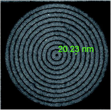 | ||
| Fig. 30 EUV patterned 20 nm circular images with 70 nm space for POM/polymer hybrid photoresist. Adapted with permission. Copyright 2015 Wiley Online Library.20 | ||
3. Challenges and future perspective
Overcoming RLS trade-off (R stands for high resolution, S for sensitivity, and L for low line edge roughness) has been the major challenge in the field of resist technology, and it will remain as the key issue in the coming days as well, till a suitable solution is achieved. Any development in this direction which addresses RLS trade-off simultaneously will be the most remarkable development in the history of resists technology for high volume manufacturing of IC chips. Considering the existing data on some of the already developed high performance resists and the problems associated with them, careful theoretical studies followed by experimental implementation may find long desired remedy.Although the multifold increment in sensitivity of many resist platforms in presence of metallic nanoparticles or hybrid metal clusters have been noticed and reported recently, the effect of pure metal clusters or metal organic frameworks have not been investigated yet. There are potentials in investigating the effect of these inorganic species on resist performance.
4. Conclusions
In conclusion, this review article provides an overview of the recent developments in the area of n-CARs, as potential replacements of CARs, for printing sub-30 nm nodes. As the CARs are approaching their limits in many aspects particularly for sub-20 nm technology, researchers are expecting drastic improvement in sub-20 nm technology with the use of n-CARs. This article focuses on the compilation of all the exciting developments, and thus provides an outline on where we stand currently with these n-CARs. Although, in many occasions, resolution and LER/LWR have been well controlled through proper resists design, but sensitivity has still been the issue for many developed n-CARs. As the n-CARs have been successfully used for printing sub-10 nm features with low LER, further improvements through structural modification of resists architecture may help to address the longstanding ‘triangle of death’ issue concerning resolution, sensitivity and LER. It is worth noting that molecular n-CARs have been quite exciting in terms of their resolution and LER.References
- H. P. alesso and C. F. Smith, Connections: patterns of discovery, John Wiley & Sons, New Jersey, 2008 Search PubMed.
- P. I. Tattersall, D. Breslin, S. M. Grayson, W. H. Heath, K. Lou, C. L. Mc Adams, D. Mc Kean, B. M. Rathsack and C. G. Willson, Chem. Mater., 2004, 16, 1770–1774 CrossRef CAS.
- B. M. Rathsack, C. E. Tabery, T. B. Stachowiak, T. E. Dallas, C. B. Xu, M. Pochkowski and C. G. Willson, Proc. SPIE, 1999, 3873, 80 CrossRef CAS.
- M. Zhao, B. Smith and T. W. Smith, Polym. Prepr., 2010, 51, 506 Search PubMed.
- J. Y. Park, J. M. Yun and J. B. Kim, J. Polym. Sci., Part A: Polym. Chem., 2008, 46, 7534–7542 CrossRef CAS.
- I. Nishimura, W. H. Heath, K. Matsumoto, W. L. Jen, S. S. Lee, C. Neikirk, T. Shimokawa, K. Ito, K. Fujiwara and C. G. Willson, Proc. SPIE, 2008, 6923, 69231C CrossRef.
- T. Chen, I. Amin and R. Jordan, Chem. Soc. Rev., 2012, 41, 3280–3296 RSC.
- C. Sanchez, P. Belleville, M. Popall and L. Nicole, Chem. Soc. Rev., 2011, 40, 696–753 RSC.
- J. Fujita, Y. Ohnishi, Y. Ochiai and S. Matsui, Appl. Phys. Lett., 1996, 68, 1297–1299 CrossRef CAS.
- H. H. Solak, Y. Ekinci and P. Käser, J. Vac. Sci. Technol., B: Microelectron. Nanometer Struct.--Process., Meas., Phenom., 2007, 25, 91–95 CrossRef CAS.
- J. Fujita, Y. Ohnishi, Y. Ochiai, E. Nomura and S. Matsui, J. Vac. Sci. Technol., B: Microelectron. Nanometer Struct.--Process., Meas., Phenom., 1996, 14, 4272–4276 CrossRef CAS.
- V. Singh, V. S. V. Satyanarayana, S. K. Sharma, S. Ghosh and K. E. Gonsalves, J. Mater. Chem. C, 2014, 2, 2118–2122 RSC.
- V. Singh, V. S. V. Satyanarayana, N. Batina, I. M. Reyes, S. K. Sharma, F. Kessler, F. R. Scheffer, D. E. Weibel, S. Ghosh and K. E. Gonsalves, J. Micro/Nanolithogr., MEMS, MOEMS, 2014, 13, 043002 CrossRef.
- V. S. V. Satyanarayana, F. Kessler, V. Singh, F. R. Scheffer, D. E. Weibel, S. Ghosh and K. E. Gonsalves, ACS Appl. Mater. Interfaces, 2014, 6, 4223–4232 CAS.
- S. Ghosh, V. S. V. Satyanarayana, B. Pramanick, S. K. Sharma, C. P. Pradeep, I. M. Reyes, N. Batina and K. E. Gonsalves, Sci. Rep., 2016, 6, 22664 CrossRef CAS PubMed.
- V. Singh, V. S. V. Satyanarayana, S. K. Sharma, S. Ghosh and K. E. Gonsalves, Proc. SPIE, 2014, 9051, 905106 CrossRef.
- V. S. V. Satyanarayana, V. Singh, S. Ghosh, S. K. Sharma and K. E. Gonsalves, Proc. SPIE, 2014, 9048, 90481W Search PubMed.
- V. Singh, V. S. V. Satynarayana, F. Kessler, F. R. Scheffer, D. E. Weibel, S. K. Sharma, S. Ghosh and K. E. Gonsalves, Proc. SPIE, 2014, 9048, 90481Y–90482Y Search PubMed.
- V. S. V. Satyanarayana, V. Singh, V. Kalyani, C. P. Pradeep, S. Sharma, S. Ghosh and K. E. Gonsalves, RSC Adv., 2014, 4, 59817–59820 RSC.
- V. Kalyani, V. S. V. Satyanarayana, V. Singh, C. P. Pradeep, S. Ghosh, S. K. Sharma and K. E. Gonsalves, Chem.–Eur. J., 2015, 21, 2250–2258 CrossRef CAS PubMed.
- V. Singh, V. Kalyani, V. S. V. Satyanarayana, C. P. Pradeep, S. Ghosh, S. Sharma and K. E. Gonsalves, Proc. SPIE, 2014, 9051, 90511W CrossRef.
- W. J. Bae, M. Trikeriotis, J. Sha, E. L. Schwartz, R. Rodriguez, P. Zimmerman, E. P. Giannelis and C. K. Ober, J. Mater. Chem., 2010, 20, 5186–5189 RSC.
- L. Li, S. Chakrabarty, K. Spyrou, C. K. Ober and E. P. Giannelis, Chem. Mater., 2015, 27, 5027–5031 CrossRef CAS.
- J. H. Sim, S. I. Lee, H. J. Lee, R. Kasica, H. M. Kim, C. L. Soles, K. B. Kim and D. Y. Yoon, Chem. Mater., 2010, 22, 3021–3023 CrossRef CAS.
- T. Nishikubo and H. Kudo, J. Photopolym. Sci. Technol., 2011, 24, 9–18 CrossRef CAS.
- J. L. Cobb, R. L. Brainard, D. J. O. Connell and P. M. Dentinger, Mater. Res. Soc. Symp. Proc., 2002, 705, 91 CAS.
- T. Kadota, H. Kageyama, F. Wakaya, K. Gomo and Y. Shirota, J. Photopolym. Sci. Technol., 1999, 12, 375–376 CrossRef CAS.
- T. Kadota, H. Kageyama, F. Wakaya, K. Gamo and Y. Shirota, Chem. Lett., 2004, 33, 706–707 CrossRef CAS.
- R. A. Lawson, L. M. Tolbert and C. L. Henderson, J. Vac. Sci. Technol., B: Microelectron. Nanometer Struct.--Process., Meas., Phenom., 2010, 28, C6S12–C6S18 CAS.
- T. Ito, A. Terao, Y. Inao, T. Yamaguchi and N. Mizutani, Proc. SPIE, 2007, 6519, 65190J CrossRef.
- R. D. Allen, R. Ayothi, L. D. Bozano, W. D. Hinsberg, L. K. Sundberg, L. S. A. Swanson, H. D. Truong, G. M. Wallraff and S. Jose, US Pat., Patent no. US 8, 900, 802 B2, 2014.
- S. M. Lee and J. M. J. Fr Bchet, Chem. Mater., 1994, 6, 1830–1837 CrossRef CAS.
- M. Yu, E. P. Giannelis and C. K. Ober, Proc. SPIE, 2016, 9779, 977905 CrossRef.
- I. Junarsa, M. P. Stoykovich, P. F. Nealey, Y. S. Ma and F. Cerrina, J. Vac. Sci. Technol., B: Microelectron. Nanometer Struct.--Process., Meas., Phenom., 2005, 23, 138–143 CrossRef CAS.
- F. Gibbons, H. M. Zaid, M. Manickam, J. A. Preece, R. E. Palmer and A. P. G. Robinson, Small, 2007, 3, 2076–2080 CrossRef CAS PubMed.
- H. Ito, Adv. Polym. Sci., 2005, 172, 37–245 CrossRef CAS.
- S. Y. Moon and J. Kim, J. Photochem. Photobiol., C, 2007, 8, 157–173 CAS.
- D. P. Sanders, Chem. Rev., 2010, 110, 321–360 CrossRef CAS PubMed.
- S. A. Mac Donald, C. G. Willson and J. M. J. Frechet, Acc. Chem. Res., 1994, 27, 151–158 CrossRef CAS.
- M. D. Stewart, K. Patterson, M. H. Somervell and C. G. Willson, J. Phys. Org. Chem., 2000, 13, 767–774 CrossRef CAS.
- E. Reichmanis and L. F. Thompson, Chem. Rev., 1989, 89, 1273–1289 CrossRef CAS.
- P. P. Naulleau, C. N. Anderson, L. M. Baclea-an, P. Denham, S. George, K. A. Goldberg, G. Jones, B. Mc Clinton, R. Miyakawa, S. Rekawa and N. Smith, Proc. SPIE, 2011, 7972, 797202 CrossRef.
- Y. Wei, M. Bender, W. D. Domke, A. Laessig, M. Sebald, S. Trogisch and D. Back, Proc. SPIE, 2007, 6519, 65190R CrossRef.
- J. W. Thackeray, J. Micro/Nanolithogr., MEMS, MOEMS, 2011, 10, 033009 CrossRef.
- T. Wallow, D. Civay, S. Wang, H. F. Hoefnagels, C. Verspaget, G. Tanriseven, A. Fumar-Pici, S. Hansen, J. Schefske, M. Singh, R. Maas, Y. van Dommelen and J. Mallmann, Proc. SPIE, 2012, 8322, 83221J CrossRef.
- R. L. Bristol, Proc. SPIE, 2007, 6519, 65190W CrossRef.
- M. Neisser and S. Wurm, Adv. Opt. Technol., 2015, 4, 235–240 Search PubMed.
- H. Wu and K. E. Gonsalves, Adv. Mater., 2001, 13, 670–672 CrossRef CAS.
- http://www.learningace.com/doc/7240269/c16fdca5b4864e58b8b64a4a051cd227/composition-and-photochemical-mechanisms-of-photoresists.
- W. M. Alvino and M. G. Hill, Plastics for electronics: materials, properties, and design applications, New York, 1995 Search PubMed.
- R. W. Blevins, R. C. Daly and S. R. Turner and J. I. Krocehwitz, Encyclopedia of Polymer Science and Engineering, Wiley & sons, New York, 1987 Search PubMed.
- L. F. Thompson, C. G. Willson and J. M. J. Frechet, Materials for Microlithography: Radiation-Sensitive Polymers, A. C. S Symposium Series, No. 266, Washington, D. C, 1984 Search PubMed.
- L. F. Thompson, C. G. Willson and S. Tagawa, Polymers for Microelectronics, A. C. S Symposium Series, No. 537, Washington, D. C, 1994 Search PubMed.
- https://www.bita.lu/datasheets/yes-20b-imagereversal.pdf.
- https://www.bita.lu/datasheets/yes-OptimizeImageReversal.pdf.
- W. W. Flack, H. A. Nguyen and E. Capsuto, Proc. SPIE, 2003, 5039, 151 CrossRef.
- M. Levanon, N. Ziona, E. Lurie, S. Malikov, O. Naigertsik, L. Postel and K. Malachi, US Pat., Patent no. US 6, 255, 033 B1, 2001.
- T. Honda, Y. Kishikawa, Y. Iwasaki, A. Okhubo, M. Kawashima and M. Yoshii, Proc. SPIE, 2006, 6154, 615422 CrossRef.
- G. M. Schmid, M. D. Stewart, C. Y. Wang, B. D. Vogt, V. M. Prabhu, E. K. Lin and C. G. Wilson, Proc. SPIE, 2004, 5376, 333 CrossRef CAS.
- K. J. Lawrie, I. Blakey, J. P. Blinco, H. H. Cheng, R. Gronheid, K. S. Jack, I. Pollentier, M. J. Leeson, T. R. Youkin and A. K. Whittaker, J. Mater. Chem., 2011, 21, 5629–5637 RSC.
- I. Blakey, L. Chen, Y. K. Goh, K. Lawrie, Y. M. Chuang, E. Piscani, P. A. Zimmerman and A. K. Whittaker, Proc. SPIE, 2009, 7273, 72733X CrossRef.
- L. Chen, Y. K. Goh, K. Lawrie, B. Smith, W. Montgomery, P. Zimmerman, I. Blakey and A. Whittaker, Proc. SPIE, 2010, 7639, 763953 CrossRef.
- L. Chen, Y. K. Goh, H. H. Cheng, B. W. Smith, P. Xie, W. Montgomery, A. K. Whittaker and I. Blakey, J. Polym. Sci., Part A: Polym. Chem., 2012, 50, 4255–4265 CrossRef CAS.
- A. Yu, H. Liu, J. P. Blinco, K. S. Jack, M. Leeson, T. R. Younkin, A. K. Whittaker and I. Blakey, Macromol. Rapid Commun., 2010, 31, 1449–1455 CrossRef CAS PubMed.
- D. C. Flanders, Appl. Phys. Lett., 1980, 36, 93–96 CrossRef CAS.
- H. H. Solak, D. He, W. Li and F. Cerrina, J. Vac. Sci. Technol., B: Microelectron. Nanometer Struct.–Process., Meas., Phenom., 1999, 17, 3052–3057 CrossRef CAS.
- T. M. Bloomstein, T. H. Fedynyshyn, I. Pottebaum, M. F. Marchant, S. J. Deneault and M. Rothschild, J. Vac. Sci. Technol., B: Microelectron. Nanometer Struct.--Process., Meas., Phenom., 2006, 24, 2789–2797 CrossRef CAS.
- S. Yasin, D. G. Hasko and H. Ahmed, Appl. Phys. Lett., 2001, 78, 2760–2762 CrossRef CAS.
- S. Yasin, D. G. Hasko and H. Ahmed, Microelectron. Eng., 2002, 61, 745–753 CrossRef.
- D. Yang, S. W. Chang and C. K. Ober, J. Mater. Chem., 2006, 16, 1693–1696 RSC.
- E. A. D. Silva, D. C. Forman and C. K. Ober, US Pat., Patent no. US7, 452, 658 B2, 2008.
- W. A. C. Bauer, C. Neuber, C. K. Ober and H. W. Schmidt, Adv. Mater., 2011, 23, 5404–5408 CrossRef CAS PubMed.
- F. Pfeiffer, N. M. Felix, C. Neuber, C. K. Ober and H. W. Schmidt, Adv. Funct. Mater., 2007, 17, 2336–2342 CrossRef CAS.
- D. L. Romero, C. A. Barrios, M. Holgado, M. F. Laguna and R. Casquel, Microelectron. Eng., 2010, 87, 663–667 CrossRef.
- T. Fujita, H. Nishihara and J. Koyama, Opt. Lett., 1981, 6, 613–615 CrossRef CAS PubMed.
- J. K. Chen, F. H. Ko, H. K. Chen, C. T. Chou, H. L. Chen and F. C. Chang, J. Vac. Sci. Technol., B: Microelectron. Nanometer Struct.--Process., Meas., Phenom., 2004, 22, 492–500 CrossRef CAS.
- S. Takei, A. Oshima, T. Wakabayashi, T. Kozawa and S. Tagawa, Appl. Phys. Lett., 2012, 101, 033106–033110 CrossRef.
- G. R. Chagas, V. S. V. Satyanarayana, F. Kessler, G. K. Belmonte, K. E. Gonsalves and D. E. Weibel, ACS Appl. Mater. Interfaces, 2015, 7, 16348–16356 CAS.
- V. C. Tejero, S. Carrasco, F. N. Villoslada, J. L. G. Fierro, M. D. C. C. Sánchez, M. C. M. Bondi and C. A. Barrios, J. Mater. Chem. C, 2013, 1, 1392–1398 RSC.
- S. Hosaka, H. Sano, M. Shirai and H. Sone, Appl. Phys. Lett., 2006, 89, 223131 CrossRef.
- B. Shokouhi, J. Zhang and B. Cui, Micro Nano Lett., 2011, 6, 992–994 CAS.
- A. Oshima, T. G. Oyama, M. Washio and S. Tagawa, Proc. SPIE, 2013, 8682, 86821A CrossRef.
- M. A. Mohammad, K. Koshelev, T. Fito, D. A. Z. Zheng, M. Stepanova and S. Dew, Jpn. J. Appl. Phys., 2012, 51, 06FC05 CrossRef.
- R. A. Lawson, C. T. Lee, W. Yueh, L. Tolbert and C. L. Henderson, Proc. SPIE, 2008, 6923, 69231I CrossRef.
- D. Bratton, R. Ayothi, H. Deng, H. B. Cao and C. K. Ober, Chem. Mater., 2007, 19, 3780–3786 CrossRef CAS.
- E. Kratschmer and M. Isaacson, J. Vac. Sci. Technol., B: Microelectron. Nanometer Struct.--Process., Meas., Phenom., 1987, 5, 369–373 CrossRef CAS.
- A. Muray, M. Scheinfein, M. Isaacson and I. Adesida, J. Vac. Sci. Technol., B: Microelectron. Nanometer Struct.--Process., Meas., Phenom., 1985, 3, 367–372 CrossRef CAS.
- C. Fujita, H. Watanabe, Y. Ochiai, S. Manako, J. S. Tsai and S. Matsui, J. Vac. Sci. Technol., B: Microelectron. Nanometer Struct.--Process., Meas., Phenom., 1995, 13, 2757–2761 CrossRef.
- M. S. M. Saifullah, K. Kurihara and C. J. Humphreys, J. Vac. Sci. Technol., B: Microelectron. Nanometer Struct.--Process., Meas., Phenom., 2000, 18, 2737–2744 CrossRef CAS.
- M. S. M. Saifullah, K. R. V. Subramanian, E. Tapley, D. J. Kang, M. E. Welland and M. Butler, Nano Lett., 2003, 3, 1587–1591 CrossRef CAS.
- M. S. M. Saifullah, K. R. V. Subramanian, D. Anderson, D. J. Kang, W. T. S. Huck, G. A. C. Jones and M. E. Welland, J. Vac. Sci. Technol., B: Microelectron. Nanometer Struct.--Process., Meas., Phenom., 2006, 24, 1215–1218 CrossRef CAS.
- A. E. Grigorescu and C. W. Hagen, Nanotechnology, 2009, 20, 292001 CrossRef CAS PubMed.
- Y. Ekinci, H. H. Solak, C. Padeste, J. Gobrecht, M. P. Stoykovich and P. F. Nealey, Microelectron. Eng., 2007, 84, 700–704 CrossRef CAS.
- V. Sidorkin, A. Grigorescu, H. Salemink and E. vander Drift, Microelectron. Eng., 2009, 86, 749–751 CrossRef CAS.
- H. Namatsu, Y. Takahashi, K. Yamazaki, T. Yamaguchi, M. Nagase and K. Kurihara, J. Vac. Sci. Technol., B: Microelectron. Nanometer Struct.--Process., Meas., Phenom., 1998, 16, 69–76 CrossRef CAS.
- M. J. Word, I. Adesida and P. R. Berger, J. Vac. Sci. Technol., B: Microelectron. Nanometer Struct.--Process., Meas., Phenom., 2003, 21, L12–L15 CrossRef CAS.
- A. E. Grigorescu, M. C. V. Krogt, C. W. Hagen and P. Kruit, Microelectron. Eng., 2007, 84, 822–824 CrossRef CAS.
- K. Ogino, J. Taniguchi, S. Satake, K. Yamamoto, Y. Ishii and K. Ishikawa, Microelectron. Eng., 2007, 84, 1071–1074 CrossRef CAS.
- T. Manabe, J. Taniguchi and K. Ishikawa, J. Vac. Sci. Technol., B: Microelectron. Nanometer Struct.--Process., Meas., Phenom., 2009, 27, 2832–2836 CrossRef CAS.
- J. Stowers and D. A. Keszler, Microelectron. Eng., 2009, 86, 730–733 CrossRef CAS.
- X. Thrun, K. H. Choi, M. Freitag, A. Grenville, M. Gutsch, C. Hohle, J. K. Stowers and J. W. Bartha, Microelectron. Eng., 2012, 98, 226–229 CrossRef CAS.
- R. P. Oleksak, R. E. Ruther, F. Luo, K. C. Fairley, S. R. Decker, W. F. Stickle, D. W. Johnson, E. L. Garfunkel, G. S. Herman and D. A. Keszler, ACS Appl. Mater. Interfaces, 2014, 6, 2917–2921 CAS.
- N. Mojarad, M. Hojeij, L. Wang, J. Gobrecht and Y. Ekinci, Nanoscale, 2015, 7, 4031–4037 RSC.
- L. Brigo, V. Auzelyte, K. A. Lister, J. Brugger and G. Brusatin, Nanotechnology, 2012, 23, 325302 CrossRef CAS PubMed.
- M. Trikeriotis, W. J. Bae, E. Schwartz, M. Krysak, N. Lafferty, P. Xie, B. Smith, P. A. Zimmerman, C. K. Ober and E. P. Giannelis, Proc. SPIE, 2010, 7639, 76390E CrossRef.
- M. Krysak, M. Trikeriotis, E. Schwartz, N. Lafferty, P. Xie, B. Smith, P. Zimmerman, W. Montgomery, E. Giannelis and C. K. Ober, Proc. SPIE, 2011, 7972, 79721C CrossRef.
- M. Trikeriotis, M. Krysak, Y. S. Chung, C. Ouyang, B. Cardineau, R. Brainard, C. K. Ober, E. P. Giannelis and K. Cho, Proc. SPIE, 2012, 8322, 83220U CrossRef.
- B. Cardineau, R. D. Re, M. Marnell, H. Al-Mashat, M. Vockenhuber, Y. Ekinci, C. Sarma, D. A. Freedman and R. L. Brainard, Microelectron. Eng., 2014, 127, 44–50 CrossRef CAS.
- R. D. Re, J. Passarelli, M. Sortland, B. Cardineau, Y. Ekinci, E. Buitrago, M. Neisser, D. A. Freedman and R. L. Brainard, J. Micro/Nanolithogr., MEMS, MOEMS, 2015, 14, 043506 CrossRef.
- J. Passarelli, M. Murphy, R. D. Re, M. Sortland, J. Hotalen, L. Dousharm, R. Fallica, Y. Ekinci, M. Neisser, D. A. Freedman and R. L. Brainard, J. Micro/Nanolithogr., MEMS, MOEMS, 2015, 14, 043503 CrossRef.
- M. Sortland, J. Hotalen, R. D. Re, J. Passarelli, M. Murphy, T. S. Kulmala, Y. Ekinci, M. Neisser, D. A. Freedman and R. L. Brainard, J. Micro/Nanolithogr., MEMS, MOEMS, 2015, 14, 043511 CrossRef.
- J. Zhang, K. Cao, X. S. Wang and B. Cui, Chem. Commun., 2015, 51, 17592–17595 RSC.
- M. T. Pope and A. Müller, Introduction to Polyoxometalate Chemistry from Topology via Self-Assembly to Applications, Kluwer, Dordrecht, 2001, pp. 1–6 Search PubMed.
| This journal is © The Royal Society of Chemistry 2016 |