DOI:
10.1039/C6RA12004K
(Paper)
RSC Adv., 2016,
6, 58950-58956
Enhanced surface and interface diffusion in Ni–Bi bilayers by swift heavy ion irradiation
Received
9th May 2016
, Accepted 3rd June 2016
First published on 7th June 2016
Abstract
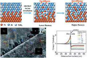
In this report, the effect of 100 MeV Au ion irradiation on diffusion in Ni/Bi bilayers has been studied. Normally, both of the layers across the interface need to reach their molten state to observe ion beam induced diffusion and mixing. However, we experimentally observed enhanced diffusion at the interface, though the thermal spike model calculations suggest that Ni does not reach its molten state at this energy regime. Spontaneous formation of a NiBi3 layer at the interface of Ni/Bi was found via the reaction–diffusion mechanism during the deposition. The evolution of porous like structures on the surface has been observed after irradiation of the films. This porous structure evolution was driven by the possible out-diffusion of Bi, as it reaches the molten state. The interface NiBi3 layer improves the mixing of the Ni and Bi layers and increases the ion fluences observed in the depth profiles obtained using cross-sectional transmission electron microscopy and Rutherford backscattering spectroscopy. Such an enhancement can be attributed to the combined swift heavy ion induced athermal effects and ballistic effects. The detailed mechanism of the ion induced surface and interface modifications were explained on the basis of thermal spike model calculations.
1 Introduction
The Ni–Bi bimetallic system is of scientific and technological importance as it shows interesting magnetic and superconducting properties once it forms alloy phases, NiBi3 (ref. 1–7) and NiBi.8,9 Of these phases, NiBi3 has been extensively studied for its superconducting behaviour1–5 for many years. This compound is also known to exhibit an interesting co-existence of superconductivity and ferromagnetism (CSF).6,7 To date, NiBi3 has been synthesized in bulk using various conventional techniques: Sakurai et al.10 co-melted high purity Ni and Bi at 900 °C for 1 hour and annealed at 480 °C and 460 °C successively for 12 hours to achieve NiBi3 stoichiometry. Fujimori et al.,2 have synthesized NiBi3 after melting the materials together for 3 days at 1100 °C in a vacuum tubular furnace. Jagdish et al.,3 and Esmeralda et al.,7 followed a similar method of preparation using temperatures around or more than 1000 °C for a longer time. We have reported, for the first time in the case of thin films, in our previous work21 the formation of a NiBi3 layer, which was spontaneously formed during the deposition of Ni/Bi bilayers.
In comparison to conventional techniques, ion beam mixing (IBM) can be a more efficient and interesting way to synthesize NiBi3, and it is a relatively low temperature process with spatial selectivity as an added advantage.11–15 Moreover, IBM can be used for the purpose of mixing even immiscible systems19, which is not possible by the other conventional techniques. The underlying mechanism of the IBM may differ, depending on the energy loss (electronic and nuclear) processes and the nature of the materials. During ion irradiation, the ions deposit energy to the material in two ways: electronic energy loss (Se) and nuclear energy loss (Sn). In the swift heavy ion (SHI) energy regime, where the Se is dominant over Sn, the mixing happens only above a threshold electronic energy loss (Seth).14,15 It should be mentioned here that a material is known to be sensitive if the Se is more than Seth and is insensitive otherwise. Therefore, the mixing will be more prominent, when both of the layers across the interface are sensitive to the ion beams.
Some work has been carried out in the context of ion beam induced modifications of Ni and Bi individually, but not on the mixing of Ni and Bi. In their studies, Wang et al.14 and Saskia et al.15 have reported that the value of Seth in the case of Ni is 77 keV nm−1 and >40 keV nm−1 respectively. Diana et al.20 have shown that Bi reaches a molten state at a value of Se which is less than the value in the present case. Since ion beam mixing of this system is not yet explored, and it may indeed reduce the synthesis time and temperature, this has motivated us to perform the present study. In the present report, we study the effect of ion beams on thermally evaporated Ni/Bi bilayers. In the as-deposited films, we found a certain amount of spontaneously formed NiBi3 layer (the details of which were discussed in our previous report21). The films were irradiated using 100 MeV Au ions at different ion fluences. Ion induced surface modifications were studied using scanning electron microscopy (SEM), while the inter-facial mixing of these layers was understood using transmission electron microscopy (TEM) and Rutherford backscattering spectroscopy (RBS). The observed surface and interfacial modifications were explained on the basis of thermal spike model calculations.
2 Experimental methods
Nickel (∼35 nm) and bismuth (∼35 nm) were subsequently deposited on a Si (100) substrate by thermal evaporation at a base pressure of below 5 × 10⁻⁷ mbar. The silicon substrates were ultrasonically cleaned, prior to deposition, using acetone followed by isopropanol and then dried thoroughly to avoid contamination. To ensure better quality of the films, a constant deposition rate of 0.01 nm s−1 and sample rotation of 20 RPM was maintained throughout the deposition and no intentional heat treatment of the substrates was employed. The bilayer films were irradiated using 100 MeV Au ions with the ion fluence varying from 1 × 10¹² to 1 × 10¹⁴ ions per cm2 at room temperature. The morphological changes of all the samples were investigated using a field emission scanning electron microscope (FESEM). Rutherford backscattering spectroscopy (RBS) measurements were carried out using 2 MeV He+ ions. Cross sectional transmission electron microscopy (XTEM) has been carried out to investigate the mixing and structural properties microscopically using a TEM (FEI, Tecnai F30) operated at 300 kV equipped with a GATAN Orius CCD camera, and energy dispersive X-ray spectroscopy (EDX) instruments. Cross-sectional TEM (XTEM) specimens were prepared using the standard method of mechanical thinning and double dimpling with final thinning using a precision-ion-polishing system (PIPS, Gatan, Pleasanton, CA). The ion polishing was carried out at 3.0 keV energy without liquid nitrogen for cooling and was followed by a 1.2 keV cleaning process. For TEM observation, specimens were aligned on [110] zone axes.
3 Results and discussions
3.1 Scanning electron microscopy
The ion induced modification of the surface morphology as a function of ion fluence is shown in Fig. 1, where panels (a), (b), (c) and (d) represent the as deposited film and the irradiated films at the fluences of 1 × 10¹² ions per cm2, 3 × 10¹² ions per cm2 and 1 × 10¹⁴ ions per cm2 respectively. The as deposited sample shows a plain surface throughout the film, while an evolution of porous like structures at the lowest fluence of 1 × 10¹² ions per cm2 can be seen. The average size of these pores are gradually increasing as a function of fluences (as shown in Fig. 2). The distribution of these pores sizes can be seen in Fig. 2(a) for the fluences 1 × 10¹² ions per cm2, 3 × 10¹² ions per cm2 and 1 × 10¹⁴ ions per cm2. In Fig. 2(b), we have shown the individual elemental mapping along with the mixing of all maps of the as deposited sample to show the distribution of elements on the surface. The insets of panels (a), (b), (c) and (d) of Fig. 1 show the corresponding magnified images. The size of the distributed particles on the surface is noticed to increase with the ion fluence, which can be due to ion beam induced local melting (as discussed in later sections). It is to be mentioned here that 100 MeV Au ions will have dominant electronic energy loss, Se, (through inelastic collisions) compared to nuclear energy loss, Sn, (through elastic collisions). The estimated values of Se and Sn, from SRIM 2008 (ref. 23), for Bi are ∼17.59, and ∼0.57 keV nm−1 respectively. It is well known that the deposited energy will be utilized in exciting the electrons of the system followed by a subsequent transfer of this energy to the lattice through electron-phonon coupling.24 During this process, high temperatures will be generated according to the thermal spike model, which can lead to mixing and alloy formation in the layers. Moreover, Bi can easily reach the molten state20 at this energy regime, as it is sensitive to swift heavy ions (explained below), which causes it to form the observed porous like structures. Therefore, we believe that the evolution of these structures is caused by the out-diffusion of Bi from the ion induced molten zones.
 |
| Fig. 1 Panels (a), (b), (c) and (d) show the scanning electron micrographs recorded on the as deposited, and irradiated films at the fluences 1 × 10¹² ions per cm2, 3 × 10¹² ions per cm2 and 1 × 10¹⁴ ions per cm2 respectively. The inset in each panel represents the magnified images of the respective samples. | |
 |
| Fig. 2 Panel (a) shows the pore size distribution as a function of ion fluence. Panel (b) represents the SEM-EDX area mapping of the as deposited sample. | |
3.2 Rutherford backscattering spectroscopy
Fig. 3 shows the RBS22 spectra of the pristine and ion irradiated samples. Particularly, the regions for Ni and Bi are shown in the inset of Fig. 3 to specify the ion induced modifications. At the high energy side of the Ni region, one can notice a tail in the case of all of the samples, which is a clear indication of the spontaneous formation of NiBi3, at the interface of Ni and Bi. The details of this spontaneous formation of NiBi3 in Ni/Bi bilayers during deposition can be found in our recent work.18,21 The estimated values of Se and Sn from SRIM 2008 (ref. 23) for Ni are ∼32.45 and ∼0.835 keV nm−1 respectively. It has been reported that Ni is insensitive to the ions in the SHI regime up to a threshold electronic energy loss (Seth) of ≥49 keV nm−1.14,15 The Se value of Ni in the present report is 32.45 keV nm−1, which is much less than the threshold value of Ni. Therefore, it is expected that the Ni layer does not reach the molten state at this energy regime. However, the estimated temperatures (from the thermal spike calculations) increase to more than ∼1000 K, which is much higher than the melting temperature of Bi and NiBi3. Hence, the top Bi and spontaneously formed NiBi3 are believed to be out-diffused from the surface. This can be noticed from the RBS spectra as the integral intensities of Bi and Ni were reduced with increasing ion fluences.
 |
| Fig. 3 RBS spectra for the pristine and irradiated samples at different fluences from 1 × 10¹² to 1 × 10¹⁴ ions per cm2. The peaks for Ni and Bi are magnified and shown in the insets. | |
Fig. 4(a) shows the depth profiles of Ni and Bi for the pristine and irradiated samples obtained from the RUMP simulations package.16 In the as-deposited sample, a uniform distribution of the top layer can be noticed until ∼50 nm from the surface, where the atomic fractions of Bi and Ni are around 0.77 and 0.23 respectively. It can be understood that the top layer is a mixture of mostly NiBi3 and partly the elemental Bi (as indicated in Fig. 4). The ratio of Ni and Bi is almost 1
:
1, in the range of 50–68 nm, which may be due to the presence of an amorphous NiBi layer or elemental Ni and Bi at the Ni/Bi interface. Beyond this depth, it is a mostly Ni layer with a small fraction of Bi. During deposition, the spontaneous formation of NiBi3 can be explained by the following eqn (1):
 |
| Fig. 4 (a) Depth profiles of Ni (solid lines) and Bi (solid lines with symbols) for the pristine and irradiated samples at different fluences from 1 × 10¹² to 1 × 10¹⁴ ions per cm2. (b) Magnified version of panel (a). The orange and green dotted arrows are representing the enhanced diffusion of Bi into Ni and Ni into Bi respectively. | |
We believe that the ion induced athermal and ballistic effects push the Ni and Bi atoms towards the interface region, which can strengthen the reaction–diffusion mechanism to enhance the mixing in the irradiated films. For clarity, the interface region of Ni and Bi was magnified and shown in Fig. 4(b). An arrow towards the right (orange in color) is shown in Fig. 4(b), which explains the enhanced Bi diffusion into Ni with the increasing ion fluence. In the same way, another arrow towards the left (green in color) is drawn to show the extra diffusion of Ni into Bi at higher fluences. It is known from the previous reports17,18 that the diffusion of Bi into Ni will be greater compared to the diffusion of Ni into Bi, which is also observed in the present study. The already existing NiBi3 layer is expected17 to enhance the mixing of Ni and Bi upon increasing the ion fluences.
3.3 Transmission electron microscopy
Fig. 5(a–c) show the cross sectional view of the pristine and irradiated samples at the fluences of 1 × 10¹² and 1 × 10¹⁴ ions per cm2 respectively and the corresponding elemental profiles are shown in panels (d), (e), and (f) which were obtained from the orange line drawn across the interfaces of the layers in panels (a), (b) and (c). These are elemental depth profiles obtained from TEM-EDX (energy dispersive analysis of X-rays) spectra. In panels (d), (e) and (f) of Fig. 5, a window of crossed lines was drawn to specify the intermixing of the layers at the respective fluences. This window in the as-deposited sample indicates an almost equal amount of Ni and Bi present at the interface (as discussed in the RBS section). The left-side region of the box is the NiBi3 region, which is spontaneously formed during deposition. These observations are in good agreement with the findings from the RBS spectra. The width of this window is gradually increasing with ion fluence, which is an indication of the improvement in the thickness of the inter-mixed region of Ni and Bi.
 |
| Fig. 5 Panels (a), (b) and (c) are the cross sectional view of the pristine and irradiated samples at the fluences of 1 × 10¹² and 1 × 10¹⁴ ions per cm2 respectively. The corresponding elemental line profiles are shown in panels (d), (e), and (f). | |
To show the enhancement in the mixing more clearly, we have recorded high resolution XTEM images of the as-deposited samples as well as the irradiated ones at the fluences of 1 × 10¹² ions per cm2 and 1 × 10¹⁴ ions per cm2. The individual Ni and Bi layers could not be distinguished in the pristine sample (Fig. 6(a)), as the layers were polycrystalline in nature. However, at the higher fluences, the difference in the layers can be clearly seen in Fig. 6(b) and (c) due to the improvement in the crystalline nature of the films. This can be understood on the basis of a large amount of energy transfer by the ions to the lattice system, at this energy regime. From the analysis of different d-spacings in the films (as shown in Fig. 6(c)), we could distinguish the individual layers in the irradiated samples. At the fluence of 1 × 10¹⁴ ions per cm2, the measured d-spacing values of NiBi3 and Ni are 2.98 Å and 2.08 Å corresponding to the (210) and (111) planes respectively. In the sample irradiated to a fluence of 1 × 10¹² ions per cm2 (Fig. 6(b)), the average thickness of Ni is found to be around 20 nm, while it reduces to almost 10 nm in the case of a sample irradiated to 1 × 10¹⁴ ions per cm2. This means that the thickness of the intermixed (NiBi3) layer is increasing with the ion fluence, which is in good agreement with the results of the elemental line profiles (mentioned above). The blue dotted lines in panels (a) and (b) are drawn to show the native oxide layer on Si, which is disappearing upon increasing the ion fluence. We did not observe any silicides of Ni in the present study (from the XRD data shown in ref. 21) even at higher fluences, as the native oxide layer on the Si substrate prevented the formation of any kind of Ni silicides even at elevated temperatures.25
 |
| Fig. 6 The cross sectional view of the HRTEM images of (a) pristine and irradiated samples at (b) 1 × 10¹² and (c) 1 × 10¹⁴ ions per cm2. The blue dashed lines are drawn at the interface of the substrate and films, while the red ones are separating Ni and NiBi3 layers. | |
3.4 Thermal spike model calculations
The underlying mechanisms of the above mentioned observations will be further explained by using thermal spike calculations.14,26–30 The calculations were performed for a combination of the present target and ion beam parameters, to discover whether the molten state at the interface is reached or not. These calculations provide the lattice temperature evolution with the elapsed time at a given distance x from the surface and a given radial distance from the ion path in the course of ion–matter interactions. This model can mathematically be represented by the following coupled eqn (2) and (3): |
 | (2) |
|
 | (3) |
where r and x are the radial distances and depth respectively. The parameters C, T, and K represent the specific heat, temperature, and thermal conductivity of the material, respectively. The suffixes a and e indicate the atomic and electronic subsystems for the corresponding physical quantities. Heat energy flow in radial (r) and depth (x) directions between the layers of different materials is taken into account by this set of equations, in both electronic and lattice subsystems, assuming a cylindrical symmetry. The lattice temperature evolution versus time was plotted in Fig. 7 for different radial distances in the case of both the bulk and multilayered system (at interface). We have also plotted the maximum lattice temperature normalized by melting point (Tmax/Tmelt) versus depth from the surface for different radial distances (Fig. 8). The physical parameters used in the thermal spike model calculations14,27,31–33 are shown in Table 1.
 |
| Fig. 7 Panels (a), (b), (c) and (d) show the evaluated lattice temperatures in Bi bulk, Bi at interface, Ni bulk and Ni at interface respectively. | |
 |
| Fig. 8 Temperature evolution at the interface of the Ni and Bi layers for different latent track radii due to the 100 MeV Au ions. | |
Table 1 Parameters used in the thermal spike calculations
Physical parameter |
Bi |
Ni |
e−-Phonon coupling g (W cm−3 K−1) |
1.35 × 10¹¹ |
1 × 10¹² |
Electronic diffusivity De (cm2 s−1) at 300 K |
38 |
150 |
Se (keV nm−1) |
17.6 |
32.4 |
Melting temperature (K) |
544 |
1726 |
Latent heat of fusion (J g−1) |
54 |
297 |
Boiling temperature (K) |
1837 |
3003 |
Latent heat of boiling (J g−1) |
491 |
6309 |
Solid density (g cm−3) |
9.81 |
8.9 |
Liquid density (g cm−3) |
10.02 |
7.9 |
For bulk materials, the calculations show that the lattice temperature in the case of Bi goes beyond its melting point (544 K) up to a radial distance of about 12 nm from the ion path (Fig. 7(a)). However, the maximum temperature reached remains less than 600 K, owing to its low electron phonon coupling constant (g = 1.35 × 10¹¹ W cm−3 K−1). For Ni (Fig. 7(c)), the lattice temperature does not exceed the melting point (1726 K), nevertheless it reaches higher values (∼1200 K) as compared to the case of Bi. For the multilayer system, the lattice temperature of Bi almost doubles at the interface compared to the bulk. The temperature increase of Bi at the interface is due to the heat flow at the interface from the Ni layer (higher temperature) to the Bi layer (lower temperature) leading to the decrease of the Ni lattice temperature near the interface as shown in Fig. 8. While the whole Bi layer undergoes a solid–liquid phase transition (Tmax/Tmelt is more than 1), the lattice temperature along the Ni layer remains lower than its melting point (Tmax/Tmelt is less than 1) which indicates that Ni is not in the molten phase. Contrary to previous thermal spike studies,33 where the molten phase could be reached from both sides of the interface of (sensitive)/(insensitive) materials leading to high mixing rates, the insensitive material (Ni) in the present study remains in the solid phase. The main reason for this is that the Bi has a low electron phonon coupling constant as compared to that of Ni. For example,33 Ni was found to reach the molten phase at the interface with titanium (Ni/Ti) where g (Ti) = 1013 W cm−3 K−1 after SHI irradiation. On the other hand, the sensitivity of Bi to SHI as confirmed by the calculations, leads to the formation of latent tracks, which may explain the porous like structures observed on the surface (as Bi is the top layer). Although not both of the materials are in the molten phase, their temperature can be considered to be high enough (1000 K, see Fig. 5(b) and (d)) to enhance atomic interdiffusion, an athermal effect, at the interface leading to the observed mixing between the Bi and Ni layers. One may not exclude the contribution of the ballistic effect34 due to nuclear stopping power.
Fig. 9 shows the enhanced surface and interface diffusion in the Ni/Bi bilayers by 100 MeV Au ion irradiation, schematically. This schematic shows the out-diffusion of Bi and Ni (from the top NiBi3 layer) as observed from RBS, which has caused the evolution of porous like structures on the surface (from SEM). As shown in the depth profiles (obtained from RBS and TEM), the mixing gets improved with increasing ion fluences. The thermal spike model calculations suggest that the temperature of the films reaches ∼1000 K, at which both the Bi and NiBi3 will definitely be in the molten phase. Though Ni does not reach the molten phase, as the Bi and NiBi3 are in contact with Ni layer for quite a bit of time, this can enhance mixing via the athermal effect. Although, a lower amount of nuclear energy deposition (Sn) also can contribute to such mixing through ballistic effects. During the process of atomic relocation due to the athermal and ballistic effects, a fraction of Ni diffuses towards the surface, while the Bi diffuses in the other direction.
 |
| Fig. 9 Schematic representation of the ion beam induced surface and interface diffusion processes in the Ni/Bi bilayers. | |
4 Conclusions
To summarize, we have studied the effect of swift heavy ion irradiation on the surface and interfacial properties of Ni/Bi bilayer films. During the deposition of these layers, we found spontaneous formation of a NiBi3 layer at the interface of Ni and Bi through a reaction–diffusion mechanism. We have noticed the development of porous like structures on the surface of films with increasing ion fluence, which is understood on the basis of out-diffusion of Bi and NiBi3 from the surface (shown in RBS). This can be understood as the local temperature of the films (from thermal spike calculations) reaches much higher than the melting point of Bi and NiBi3. The thickness of the NiBi3 layer increases with ion fluence which is confirmed by depth profiles. Although the Ni and Bi are insensitive/sensitive materials to ion beams, respectively, the spontaneously formed NiBi3 layer helps to improve the diffusion process in mixing the layers during ion irradiation. The enhancement in the mixing of Ni and Bi with increasing ion fluence has been attributed to the combination of athermal (driven by molten phases) and ballistic (caused by nuclear stopping) effects along with a reaction-diffusion process. The synthesis of mixed layers of Ni, Bi and NiBi3 might be applicable where technologies need both superconducting and ferromagnetic materials.
Acknowledgements
The authors acknowledge the funding from National Institute of Science Education and Research (NISER), Department of Atomic Energy (DAE), India. The authors are thankful to Dr Kartik Senapati, SPS, NISER Bhubaneswar and Dr D. K. Avasthi, IUAC for their fruitful discussions.
References
- N. Alekseevskii, J. Exp. Theor. Phys., 1948, 18, 101 CAS.
- Y. Fujimori, S. Kan, B. Shinozaki and T. Kawaguti, J. Phys. Soc. Jpn., 2000, 69, 3017 CrossRef CAS.
- J. Kumar, A. Kumar, A. Vajpayee, B. Gahtori, D. Sharma, P. K. Ahluwalia, S. Auluck and V. P. S. Awana, Supercond. Sci. Technol., 2011, 24, 085002 CrossRef.
- X. Zhu, H. Lei, C. Petrovic and Y. Zhang, Phys. Rev. B: Condens. Matter Mater. Phys., 2012, 86, 024527 CrossRef.
- B. Silva, R. F. Luccas, N. M. Nemes, J. Hanko, M. R. Osorio, P. Kulkarni, F. Mompean, M. García-Hernández, M. A. Ramos, S. Vieira and H. Suderow, Phys. Rev. B: Condens. Matter Mater. Phys., 2013, 88, 184508 CrossRef.
- T. Herrmannsdorfer, R. Skrotzki, J. Wosnitza, D. Kohler, R. Boldt and M. Ruck, Phys. Rev. B: Condens. Matter Mater. Phys., 2011, 83, 140501 CrossRef.
- E. L. M. Piñeiro, B. L. R. Herrera, R. Escudero and L. Bucio, Solid State Commun., 2011, 151, 425 CrossRef.
- H. Yoshida, T. Shima, T. Takahashi, T. Kaneko, T. Suzuki, H. M. Kimura, K. Asami and A. Inoue, J. Magn. Magn. Mater., 2002, 239, 5 CrossRef CAS.
- S. Park, K. Kang, W. Han and T. Vogt, J. Alloys Compd., 2005, 400, 88 CrossRef CAS.
- M. Sakurai, T. Ono, I. Yoshida and S. Tanuma, Jpn. J. Appl. Phys., 2000, 39, 6366 CrossRef CAS.
- M. Nastasi and J. W. Mayer, Mater. Sci. Eng., R, 1994, 12, 1 CrossRef.
- S. J. Kim, M. A. Nicolet, R. S. Averback and D. Peak, Phys. Rev. B: Condens. Matter Mater. Phys., 1988, 37, 38 CrossRef CAS.
- S. K. Srivastava, R. Kumar, A. Gupta, R. S. Patel, A. K. Majumdar and D. K. Avasthi, Nucl. Instrum. Methods Phys. Res., Sect. B, 2006, 243, 304 CrossRef CAS.
- Z. G. Wang, C. Dufour, E. Paumier and M. Toulemoude, J. Phys.: Condens. Matter, 1994, 6, 6733 CrossRef CAS.
- S. Kraft, B. Schattat, W. Bolse, S. Klaumünzer, F. Harbsmeier, A. Kulinska and A. Lffl, J. Appl. Phys., 2002, 91, 1129 CrossRef CAS.
- L. R. Doolittle, RUMP: Rutherford backscattering spectroscopy analysis package, Nucl. Instrum. Methods Phys. Res., Sect. B, 1985, 9, 344 CrossRef.
- V. I. Dybkov, in Solid State Reaction Kinetics, IMPS Publications, Kyiv, Ukraine, 2013 Search PubMed.
- V. Siva, P. C. Pradhan, G. S. Babu, M. Nayak, P. K. Sahoo and K. Senapati, J. Appl. Phys., 2016, 119, 063902 CrossRef.
- S. Amirthapandian, B. K. Panigrahi, A. K. Srivastava, S. Dhara, A. Gupta, V. S. Sastry, R. V. Nandedkar, K. G. M. Nair and A. Narayanasamy, J. Appl. Phys., 2004, 95, 5295 CrossRef CAS.
- T. Diana, D. C. Agarwal, P. K. Kulriya, S. K. Tripathi and H. Nandakumar Sarma, Adv. Mater. Lett., 2014, 5, 223 CrossRef.
- V. Siva, K. Senapati, B. Satpati, S. Prusty, D. K. Avasthi, D. Kanjilal and P. K. Sahoo, J. Appl. Phys., 2015, 117, 083902 CrossRef.
- W. K. Chu, J. W. Mayer and M. A. Nicolet, Backscattering Spectrometry, Academic, Orlando, 1978 Search PubMed.
- J. F. Ziegler, M. D. Ziegler and J. P. Biersack, Nucl. Instrum. Methods Phys. Res., Sect. B, 2010, 268, 1818 CrossRef CAS.
- D. K. Avasthi, W. Assmann, A. Tripathi, S. K. Srivastava, S. Ghosh, F. Gruner and M. Toulemonde, Phys. Rev. B: Condens. Matter Mater. Phys., 2003, 68, 153106 CrossRef.
- P. S. Lee, D. Mangelinck, K. L. Pey, J. Ding, J. Y. Dai, C. S. Ho and A. See, Microelectron. Eng., 2000, 51, 583 CrossRef.
- Z. G. Wang, C. Dufour, E. Paumier and M. Toulemonde, J. Phys.: Condens. Matter, 1995, 7, 2525 CrossRef CAS.
- C. Dufour, Z. G. Wang, E. Paumier and M. Toulemonde, Bull. Mater. Sci., 1999, 22, 671 CrossRef CAS.
- A. Chettah, Z. G. Wang, M. Kac, H. Kucal, A. Meftah and M. Toulemonde, Nucl. Instrum. Methods Phys. Res., Sect. B, 2006, 245, 150 CrossRef CAS.
- M. Toulemonde, C. Dufour, Z. G. Wang and E. Paumier, Nucl. Instrum. Methods Phys. Res., Sect. B, 1996, 112, 26 CrossRef CAS.
- M. Toulemonde, C. Dufour and E. Paumier, Phys. Rev. B: Condens. Matter Mater. Phys., 1992, 46, 14362 CrossRef.
- C. Dufour, A. Audouard, F. Beuneu, J. Dural, J. P. Girard, A. Hairie, M. Levalois, E. Paumier and M. Toulemonde, J. Phys.: Condens. Matter, 1993, 5, 4573 CrossRef CAS.
- C. Dufour, F. Beuneu, E. Paumier and M. Toulemonde, Europhys. Lett., 1999, 45(5), 585–590 CrossRef CAS.
- Z. G. Wang, C. Dufour, S. Euphrasie and M. Toulemonde, Nucl. Instrum. Methods Phys. Res., Sect. B, 2003, 209, 194 CrossRef CAS.
- D. K. Avasthi and G. K. Mehta, Springer Series in Material Science, 145, Springer Science and Business Media, 2011 Search PubMed.
|
This journal is © The Royal Society of Chemistry 2016 |
Click here to see how this site uses Cookies. View our privacy policy here.