Stimulated emission at 272 nm from an AlxGa1−xN-based multiple-quantum-well laser with two-step etched facets
Yingdong Tian ,
Yun Zhang*,
Jianchang Yan,
Xiang Chen,
Junxi Wang and
Jinmin Li*
Semiconductor Lighting Technology Research and Development Center, Institute of Semiconductors, Chinese Academy of Sciences, Beijing 100083, China. E-mail: yzhang34@semi.ac.cn; jmli@semi.ac.cn
First published on 18th May 2016
Abstract
We developed a two-step facet etching method combining inductively coupled plasma etching and KOH-based wet-etching surface treatment to achieve vertical and smooth facets for AlGaN-based ultraviolet (UV) multiple-quantum-well lasers on sapphire substrates. Stimulated emission at 272 nm was observed by optical pumping on both lasers with cleaved facets and two-step-etched facets with line widths of 1.3 nm and 0.4 nm, respectively. Compared to the laser with cleaved facets, the threshold optical power density of the laser with two-step-etched facets significantly reduced from 520 kW cm−2 to 350 kW cm−2, and the differential quantum efficiency increased onefold. Further analysis shows that the better performance of the two-step-etched AlGaN-based UV laser mainly results from the smooth and uniform facets after the wet-etching surface treatment, which is an effective and controllable approach combined with dry etching for laser facet fabrication.
Introduction
Ultraviolet (UV) lasers have plenty of applications, such as high-density optical storage, biochemical detection, sensing and medical treatments, etc. Thanks to their direct and wide semiconductor bandgap, AlxGa1−xN-based materials are attracting significant attention as ideal candidates to fabricate the next-generation UV semiconductor laser devices.1 Achieving high-quality high-Al-content AlGaN epitaxial materials is one of the challenges for stimulated emission in deep ultraviolet (DUV) lasers. With remarkable progress on the high-Al-content AlGaN epitaxy technology, optically pumped AlxGa1−xN-based lasers with cleaved Fabry–Perot (F–P) resonance cavities have been demonstrated on SiC, AlN and sapphire substrates in the DUV band.2–8 On the other hand, the vertical and mirror-like cavity facet with high reflectivity is also a key factor for a high-quality F–P laser, playing an important role in reducing lasing threshold and improving reliability. However, facet fabrication methods are relatively less explored, especially for AlxGa1−xN on sapphire substrates with advantages of mature AlxGa1−xN epitaxy technology, low cost, adjustable size and unlimited availability. Until now the electrical pump deep UV lasers are still elusive, and the shortest wavelength for the UV lasers is 336 nm.9–11 It is difficult to achieving high p-type conductivity for cladding layers, and the optical pump is an necessary stage for realization of the electrical pumped deep UV lasers. Although all the reported optically pumped AlxGa1−xN-based sub-300 nm DUV lasers on sapphire substrates employed cleaved facets,5,7,8 the cleaving method is not the optimum choice for AlxGa1−xN laser wafers grown on sapphire substrates since the surfaces of cleaving will be stepped and striated due to the 30° rotation of AlxGa1−xN unit cell relative to c-plane sapphire substrate. Dry etching is an alternative ways to form facets for GaN-based lasers,12–16 owning the advantages for the AlGaN epitaxial layers grown on substrate that do not share the same cleavage planes, including heteroepitaxial growth and semipolar or nonpolar substrates, in addition to the potential for on-wafer optoelectronic integration. However, the ion bombardment damage during dry etching will make the laser facet surface roughness as large as several tens nanometer.14,17 To address this issue, certain facet treatment process following dry etching is necessary to obtain an atomic smooth facet.In this work, we developed a two-step facet forming method consisting of an inductively coupled plasma (ICP) etching with Ni metal as an etching mask to define the cavity length of the laser bars, followed by crystallographic wet etching in heated KOH based solution to reduce the roughness and improve verticality of the sidewall. Smooth and vertical facets for AlGaN-based MQWs lasers grown on sapphire substrate were formed via the carefully optimization of dry etching and wet chemical etching process. We also demonstrated the first AlGaN-based DUV MQW laser grown on sapphire substrates with facets prepared by etching, not cleaving, which will offer more smoothness and uniformity. Lasing behaviors at the stimulated emission wavelength of 272 nm with narrow line width of 0.4 nm was accomplished on the laser bars with two-step etched facets. Compared to the laser with direct-cleaved facets, the two-step facet forming method significantly reduced the lasing threshold from 520 kW cm−2 to 350 kW cm−2 with a onefold improvement of differential quantum efficiency. X-ray diffraction (XRD), atomic-force microscopy (AFM) and cross-sectional transmission electron microscopy (TEM) were carried out to evaluate the crystalline quality of the laser structure. Scan electronic microscope (SEM) was performed to check the sidewall appearance for the optimization of dry and wet etching process.
Experiments
The AlGaN-based DUV laser structure was grown on a c-plane sapphire substrate using a homemade metal–organic chemical vapor deposition (MOCVD) system with a growth pressure of 50 Torr. Trimethylaluminum, trimethylgallium and ammonia were the precursors and hydrogen was the carrier gas. Fig. 1(a) is the schematic diagram of the AlGaN-based DUV laser. The epitaxial process began with a 50 nm AlN buffer layer grown at 735 °C after 2 minutes annealing at 1010 °C, and a 1.4 μm AlN template was grown at 1200 °C with a growth rate of 1 μm hour−1. The full width at half maximum (FWHM) values for (0002) and (10![[1 with combining macron]](https://www.rsc.org/images/entities/char_0031_0304.gif) 2) reflections are 60 arcsec and 450 arcsec, respectively, so the screw and edge dislocation densities are estimated to be 7.8 × 106 cm−2 and 2.4 × 109 cm−2, respectively.18 AFM measurement shows that the root-mean-square (RMS) surface roughness is 0.306 nm on a 10 × 10 μm2 square with a step-flow growth mode. The MQWs were grown above the AlN template at 1080 °C consisting of 6 pairs of 2.5 nm Al0.55Ga0.45N and 9 nm AlN, and the whole epitaxy finished with a 60 nm AlN cap for optical confinement and surface passivation. The thicknesses of AlGaN MQWs layers and cap layer were optimized with waveguide modeling simulation to improve optical confinement. The optical field distribution of the fundamental waveguide mode was shown in Fig. 1(b) and the optical confinement factor (Γ) was calculated to be 11.57%. The refractive indices for ternary AlGaN alloys are taken from ref. 19. The maximum of optical field distribution located at the center of the active area, and little optical mode was found to leak outside the active region owning to the AlN cap layer.
2) reflections are 60 arcsec and 450 arcsec, respectively, so the screw and edge dislocation densities are estimated to be 7.8 × 106 cm−2 and 2.4 × 109 cm−2, respectively.18 AFM measurement shows that the root-mean-square (RMS) surface roughness is 0.306 nm on a 10 × 10 μm2 square with a step-flow growth mode. The MQWs were grown above the AlN template at 1080 °C consisting of 6 pairs of 2.5 nm Al0.55Ga0.45N and 9 nm AlN, and the whole epitaxy finished with a 60 nm AlN cap for optical confinement and surface passivation. The thicknesses of AlGaN MQWs layers and cap layer were optimized with waveguide modeling simulation to improve optical confinement. The optical field distribution of the fundamental waveguide mode was shown in Fig. 1(b) and the optical confinement factor (Γ) was calculated to be 11.57%. The refractive indices for ternary AlGaN alloys are taken from ref. 19. The maximum of optical field distribution located at the center of the active area, and little optical mode was found to leak outside the active region owning to the AlN cap layer.
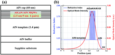 | ||
| Fig. 1 (a) The schematic diagram for AlGaN-based MQWs UV laser; (b) the refractive index profile and simulated optical field distribution within the laser structure. | ||
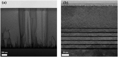
Asymmetric (10![[1 with combining macron]](https://www.rsc.org/images/entities/char_0031_0304.gif) 5) reciprocal space mapping was carried out to analyze the strain in the MQWs and AlN cap layers indicating that these layers were fully strained with respect to the underlying AlN template, thereby inhibiting dislocation generation associated with lattice relaxation. The cross-sectional TEM image in Fig. 2(a) also confirmed that no additional TDs were brought in the pseudomorphically epitaxial layers. Moreover, Fig. 2(a) revealed that some TDs terminated during the AlN template layer growth and did not extend to the active area. The TEM image of MQWs shown in Fig. 2(b) confirmed the thicknesses of quantum wells and barriers.
5) reciprocal space mapping was carried out to analyze the strain in the MQWs and AlN cap layers indicating that these layers were fully strained with respect to the underlying AlN template, thereby inhibiting dislocation generation associated with lattice relaxation. The cross-sectional TEM image in Fig. 2(a) also confirmed that no additional TDs were brought in the pseudomorphically epitaxial layers. Moreover, Fig. 2(a) revealed that some TDs terminated during the AlN template layer growth and did not extend to the active area. The TEM image of MQWs shown in Fig. 2(b) confirmed the thicknesses of quantum wells and barriers.
Subsequent to the growth process, laser cavities with cavity lengths of 1 mm were fabricated by two different methods for comparison, the cleaving method and a two-step etching method. The width of the laser resonator was fixed to the width of the incidence beam, which is set to 400 μm. The cleaving method was performed by cleaving the sample along the [11![[2 with combining macron]](https://www.rsc.org/images/entities/char_0032_0304.gif) 0] a-direction assisted by a 355 nm laser scriber to form m-plane facets. The thickness of the sapphire substrate was 330 μm and the depth of the laser scribing was about 100 μm on the backside. A typically rugged cleaved facet was checked in SEM, while the crack commonly extend to the top active region of the structure, and which was catastrophic to the formation of resonant cavity. The stepped facet with terrenes resulted from stress between AlN epitaxial layer and sapphire substrate. Some cleaved facet can also turn out with smooth surface, and the suitable facet is smooth, stria free and shows a considerable low RMS roughness. Steps and terraces do not penetrate into the active region, however, the good area checked in SEM showed random distribution without continuity in the laser bar.
0] a-direction assisted by a 355 nm laser scriber to form m-plane facets. The thickness of the sapphire substrate was 330 μm and the depth of the laser scribing was about 100 μm on the backside. A typically rugged cleaved facet was checked in SEM, while the crack commonly extend to the top active region of the structure, and which was catastrophic to the formation of resonant cavity. The stepped facet with terrenes resulted from stress between AlN epitaxial layer and sapphire substrate. Some cleaved facet can also turn out with smooth surface, and the suitable facet is smooth, stria free and shows a considerable low RMS roughness. Steps and terraces do not penetrate into the active region, however, the good area checked in SEM showed random distribution without continuity in the laser bar.
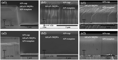
The two-step facet etching process consisted of ICP etching followed by crystallographic wet-etching surface treatment to reduce roughness and improve facet verticality. A layer of nickel was patterned into 1 mm stripes aligned in [11![[2 with combining macron]](https://www.rsc.org/images/entities/char_0032_0304.gif) 0] a-direction as ICP-etching mask for m-plane facets. The ICP coil power and platen power were 450 W and 50 W, and the gas flow rates were 25/25/5 sccm for Cl2/BCl3/Ar, respectively. The gas flow rate of Cl2/Ar strongly affected the facet angle, but the RF power and the gas flow rate of BCl3 were not the key factor. The facet angle was 3° from vertical as shown in Fig. 3(a1). In Fig. 3(b1), the sloped and striated facet of ICP etching was originated from ion bombardment. Both the facet tilt and roughness can significantly degrade the reflectivity on the AlGaN/air interface, and this issue has to be addressed by further treatment.
0] a-direction as ICP-etching mask for m-plane facets. The ICP coil power and platen power were 450 W and 50 W, and the gas flow rates were 25/25/5 sccm for Cl2/BCl3/Ar, respectively. The gas flow rate of Cl2/Ar strongly affected the facet angle, but the RF power and the gas flow rate of BCl3 were not the key factor. The facet angle was 3° from vertical as shown in Fig. 3(a1). In Fig. 3(b1), the sloped and striated facet of ICP etching was originated from ion bombardment. Both the facet tilt and roughness can significantly degrade the reflectivity on the AlGaN/air interface, and this issue has to be addressed by further treatment.
To realize vertical and mirror-like facets, wet-etching treatment was carried out on the ICP-etched facets in diluted KOH-based solution at 70 °C. The selective crystallographically etching feature on AlN and AlGaN materials of KOH solution, preferentially exposing the (10![[1 with combining macron]](https://www.rsc.org/images/entities/char_0031_0304.gif) 0) owning to their slow etch rates compared with the other planes, providing the path to recovery of smooth uniform crystal planes.11,17,18 The laser facets were designed to parallel the (10
0) owning to their slow etch rates compared with the other planes, providing the path to recovery of smooth uniform crystal planes.11,17,18 The laser facets were designed to parallel the (10![[1 with combining macron]](https://www.rsc.org/images/entities/char_0031_0304.gif) 0) plane with the exposure of the (10
0) plane with the exposure of the (10![[1 with combining macron]](https://www.rsc.org/images/entities/char_0031_0304.gif) 0) and (10
0) and (10![[1 with combining macron]](https://www.rsc.org/images/entities/char_0031_0304.gif) n)-type planes after the ICP etching process. AlGaN-based etched sidewalls with streaks, as showed in Fig. 3(b1), will be abound with defective bonds that are more easily to attack by the OH− in the developer solution. The selective crystallographic etching of KOH combined with intended exposure of m-plane facet removed the fibrous texture originated from plasma to improve the local smoothness as well as the entire uniformity of these facets. In the wet etching process, the facets along 〈11
n)-type planes after the ICP etching process. AlGaN-based etched sidewalls with streaks, as showed in Fig. 3(b1), will be abound with defective bonds that are more easily to attack by the OH− in the developer solution. The selective crystallographic etching of KOH combined with intended exposure of m-plane facet removed the fibrous texture originated from plasma to improve the local smoothness as well as the entire uniformity of these facets. In the wet etching process, the facets along 〈11![[2 with combining macron]](https://www.rsc.org/images/entities/char_0032_0304.gif) 0〉 direction became smooth and vertical while the stripe along 〈10
0〉 direction became smooth and vertical while the stripe along 〈10![[1 with combining macron]](https://www.rsc.org/images/entities/char_0031_0304.gif) 0〉 direction became rougher with many triangular shapes, which is more likely to be (10
0〉 direction became rougher with many triangular shapes, which is more likely to be (10![[1 with combining macron]](https://www.rsc.org/images/entities/char_0031_0304.gif) 0) planes, confirming the slower etching rate of hydroxide ions (OH−) on (10
0) planes, confirming the slower etching rate of hydroxide ions (OH−) on (10![[1 with combining macron]](https://www.rsc.org/images/entities/char_0031_0304.gif) 0) plane compared with (11
0) plane compared with (11![[2 with combining macron]](https://www.rsc.org/images/entities/char_0032_0304.gif) 0) plane.20 The two-step process is thus notably superior to plasma etching alone. Longer exposure of up to 25 min in the 70 °C KOH-based solution exposed the smooth and vertical (10
0) plane.20 The two-step process is thus notably superior to plasma etching alone. Longer exposure of up to 25 min in the 70 °C KOH-based solution exposed the smooth and vertical (10![[1 with combining macron]](https://www.rsc.org/images/entities/char_0031_0304.gif) 0) plane with a foot-like trench at the bottom of the etching sidewall. The nickel mask was removed by acid after the wet-etching treatment. The two-step facet etching process successfully fabricated vertical laser facets with mirror-like surface as shows in Fig. 3(a2) and (b2). The fibrous texture originated from plasma etching annihilated in the wet etching process, and the Fig. 3(b2) demonstrates the 10° tilt view of etched m-plane facet with considerable smoothing. Moreover, the laser with two-step etched facets had higher overall uniformity than those of cleaved laser because of the controllable semiconductor state of art, with additional wet etching procedure.
0) plane with a foot-like trench at the bottom of the etching sidewall. The nickel mask was removed by acid after the wet-etching treatment. The two-step facet etching process successfully fabricated vertical laser facets with mirror-like surface as shows in Fig. 3(a2) and (b2). The fibrous texture originated from plasma etching annihilated in the wet etching process, and the Fig. 3(b2) demonstrates the 10° tilt view of etched m-plane facet with considerable smoothing. Moreover, the laser with two-step etched facets had higher overall uniformity than those of cleaved laser because of the controllable semiconductor state of art, with additional wet etching procedure.
Results and discussions
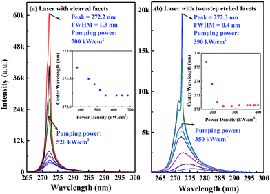
The edge emission spectra of the cleaved facet laser and the two-step-etched facet laser pumped are plotted in Fig. 4(a) and (b) by varied optical power. The pumping source was a KrF excimer laser (λ = 248 nm) whose optical power was adjusted by filters. The incidence beam size was 400 μm × 2200 μm set by a manual slit and the pulse width was 20 ns with repetition frequency of 5 Hz. An Ocean Optics Maya 2000 Pro spectrometer recorded the emission spectra through a UV fiber placed 5 cm in front of laser facets. When the optical pumping power density was low, the edge emission spectra of both lasers exhibited a spontaneous emission at around 273 nm with FWHM > 10 nm. Both these lasers showed a blue shift of the central wavelength along with the increasing pumping power density, which might originate from a gradual filling of localized states, as well as the reduction of quantum confined stark effect due to the screening of polarization charges. With the pumping power increasing to about 520 kW cm−2, a narrow emission peak dominated the spectra with the FWHM dropped to 3 nm for the cleaved laser, as shown in Fig. 4(a). For the laser with two-step etched facets, when the pumping power increased to about 350 kW cm−2, a sharp emission peak emerged on top of the spontaneous emission peak. The sharp and narrow emission peak increased drastically while the broad spontaneous emission increased tardily at higher pumping power. The drastically increasing intensity of the sharp emission peak over the spontaneous emission confirmed that the emitted emission amplified via stimulated emission. Because of the stronger re-absorption at the high-energy parts of the spontaneous emission spectrum, the stimulated emission related peak located at the long wavelength side of the broad spontaneous emission peak. When the optical pumping power went higher beyond the threshold threshold power density (Pth), stimulated emission at 272.2 nm and 272.3 nm was observed on both lasers with cleaved facets and two-step etched facets with FWHM of 1.3 nm and 0.4 nm, respectively. Under higher excitation, the intensity of the edge emitting spectra did not increased as the increase of the pump power. Further increase in pump power, the lasers would burn.As shown in Fig. 5, the spectral integrated intensity is plotted versus the optical pumping power density for both lasers. Lasing behavior is observed on both lasers beyond the Pth. Compared to the laser with cleaved facets, the Pth of the laser with two-step etched facets significantly reduces from 520 kW cm−2 to 350 kW cm−2, and the differential quantum efficiency (ηd) increases onefold. While in the optical pumping experiments, the pumping condition is setting the same, and these two laser samples were chosen in the near position to guarantee the same material quality. The surface condition of these two laser samples were the same in the experiments, together with the same optical pumping condition, which made the same coupling condition. The only difference between these two samples was the facet fabrication method, resulting in different reflectivity. Therefore, the 33% reduction of the pump threshold is attributed to a better reflectivity of the facets, other than the better coupling. The performance enhancement mechanism is explained below. The threshold modal gain (gth) and ηd can be calculated21 by following equations:
| Γgth = 〈αi〉 + αm | (1) |
 | (2) |
 | (3) |
 | (4) |
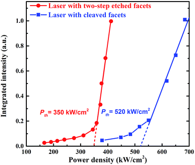 | ||
| Fig. 5 Spectral integrated intensity as function of pumping power densities with different facet fabrication (red: laser with two-step-etched facets; blue: laser with cleaved facets). | ||
Conclusion
In conclusion, we developed a two-step facet etching method consisting of ICP etching followed by crystallographic wet etching in KOH-based solution, and demonstrated AlGaN-based DUV MQW laser grown on sapphire substrates. Lasing behaviors of a single longitudinal mode at 272.3 nm with a narrow line width of 0.4 nm was obtained on the laser bar with two-step etched facets. The threshold power density is 350 kW cm−2, 33% lower than that of the laser with cleaved facets. To the best of our knowledge, it is the first optically pumped AlGaN-based DUV lasers whose facets were not prepared by cleaving. The lower threshold and higher differential quantum efficiency of the laser with two-step etched facets are because of the additional wet etching procedure that can effectively reduce roughness and improve verticality on the facets.Acknowledgements
This work was supported the National Natural Sciences Foundation of China under Grant No. 61376047, No. 61006038, No. 61204052, No. 61206090 and No. 61204053. National High Technology Program of China under Grant No. 2014AA032608 also supported this work.Notes and references
- M. Kneissl, T. Kolbe, C. Chua, V. Kueller, N. Lobo, J. Stellmach, A. Knauer, H. Rodriguez, S. Einfeldt, Z. Yang, N. M. Johnson and M. Weyers, Semicond. Sci. Technol., 2011, 26, 014036 CrossRef.
- T. Takano, Y. Narita, A. Horiuchi and H. Kawanishi, Appl. Phys. Lett., 2004, 84, 3567–3569 CrossRef CAS.
- T. Wunderer, C. Chua, J. Northrup, Z. Yang, N. Johnson, M. Kneissl, G. Garrett, H. Shen, M. Wraback and B. Moody, Phys. Status Solidi C, 2012, 9, 822–825 CrossRef CAS.
- Z. Lochner, T.-T. Kao, Y.-S. Liu, X.-H. Li, M. M. Satter, S.-C. Shen, P. D. Yoder, J.-H. Ryou, R. D. Dupuis, Y. Wei, H. Xie, A. Fischer and F. A. Ponce, Appl. Phys. Lett., 2013, 102, 101110–101114 CrossRef.
- M. Martens, F. Mehnke, C. Kuhn, C. Reich, V. Kueller, A. Knauer, C. Netzel, C. Hartmann, J. Wollweber, J. Rass, T. Wernicke, M. Bickermann, M. Weyers and M. Kneissl, IEEE Photonics Technol. Lett., 2014, 26, 342–345 CrossRef CAS.
- J. Xie, S. Mita, Z. Bryan, W. Guo, L. Hussey, B. Moody, R. Schlesser, R. Kirste, M. Gerhold, R. Collazo and Z. Sitar, Appl. Phys. Lett., 2013, 102, 171102–171104 CrossRef.
- F. Asif, M. Lachab, A. Coleman, I. Ahmad, B. Zhang, V. Adivarahan and A. Khan, J. Vac. Sci. Technol., B: Nanotechnol. Microelectron.: Mater., Process., Meas., Phenom., 2014, 32, 061204 Search PubMed.
- X.-H. Li, T. Detchprohm, T.-T. Kao, M. M. Satter, S.-C. Shen, P. Douglas Yoder, R. D. Dupuis, S. Wang, Y. O. Wei, H. Xie, A. M. Fischer, F. A. Ponce, T. Wernicke, C. Reich, M. Martens and M. Kneissl, Appl. Phys. Lett., 2014, 105, 141106 CrossRef.
- M. Martens, C. Kuhn, E. Ziffer, T. Simoneit, V. Kueller, A. Knauer, J. Rass, T. Wernicke, S. Einfeldt, M. Weyers and M. Kneissl, Appl. Phys. Lett., 2016, 108, 151108 CrossRef.
- H. Yoshida, Y. Yamashita, M. Kuwabara and H. Kan, Nat. Photonics, 2008, 2, 551–554 CrossRef CAS.
- H. Yoshida, Y. Yamashita, M. Kuwabara and H. Kan, Appl. Phys. Lett., 2008, 93, 241106 CrossRef.
- T. Böttcher, C. Zellweger, S. Figge, R. Kröger, C. Petter, H. J. Bühlmann, M. Ilegems, P. Ryder and D. Hommel, Phys. Status Solidi A, 2002, 191, R3–R5 CrossRef.
- M. Kneissl, D. W. Treat, M. Teepe, N. Miyashita and N. M. Johnson, Appl. Phys. Lett., 2003, 82, 4441–4443 CrossRef CAS.
- M. Itoh, T. Kinoshita, C. Koike, M. Takeuchi, K. Kawasaki and Y. Aoyagi, Jpn. J. Appl. Phys., 2006, 45, 3988–3991 CrossRef CAS.
- M. Kneissl, Z. Yang, M. Teepe, C. Knollenberg, O. Schmidt, P. Kiesel, N. M. Johnson, S. Schujman and L. J. Schowalter, J. Appl. Phys., 2007, 101, 123103 CrossRef.
- H. Yoshida, Y. Yamashita, M. Kuwabara and H. Kan, Nat. Photonics, 2008, 2, 551–554 CrossRef CAS.
- M. A. Miller, M. H. Crawford, A. A. Allerman, K. C. Cross, M. A. Banas, R. J. Shul, J. Stevens and K. H. A. Bogart, J. Electron. Mater., 2009, 38, 533–537 CrossRef CAS.
- B. N. Pantha, R. Dahal, M. L. Nakarmi, N. Nepal, J. Li, J. Y. Lin, H. X. Jiang, Q. S. Paduano and D. Weyburne, Appl. Phys. Lett., 2007, 90, 241101 CrossRef.
- D. Brunner, H. Angerer, E. Bustarret, F. Freudenberg, R. Höpler, R. Dimitrov, O. Ambacher and M. Stutzmann, J. Appl. Phys., 1997, 82, 5090 CrossRef CAS.
- C. Vartuli, S. Pearton, J. Lee, C. Abernathy, J. MacKenzie, J. Zolper, R. Shul and F. Ren, J. Electrochem. Soc., 1996, 143, 3681–3684 CrossRef CAS.
- L. A. Coldren, S. W. Corzine and M. L. Mashanovitch, Diode lasers and photonic integrated circuits, John Wiley & Sons, 2012 Search PubMed.
- J. Yun, J.-I. Shim and H. Hirayama, Appl. Phys. Express, 2015, 8, 022104 CrossRef.
| This journal is © The Royal Society of Chemistry 2016 |

