
 Open Access Article
 This Open Access Article is licensed under a Creative Commons Attribution-Non Commercial 3.0 Unported Licence
Resistive hysteresis in flexible nanocomposites and colloidal suspensions: interfacial coupling mechanism unveiled†
A. Chiolerio*a,
I. Roppoloa,
K. Bejtkaa,
A. Asvarovab and
C. F. Pirria
aCenter for Space Human Robotics, Istituto Italiano di Tecnologia, Corso Trento 21, 10129 Torino, Italy. E-mail: alessandro.chiolerio@iit.it
bInstitute of Physics, Dagestan Scientific Center, Russian Academy of Sciences, Yaragskogo Str. 94, Makhackhala 367003, Russia
First published on 31st May 2016
Abstract
A route for the preparation of nanocomposite flexible devices featuring resistive hysteresis, based on zinc oxide and UV curable polymers, was developed. A new phenomenon involving interfacial exchange was isolated and proven, exploring the phase space of matrices and fillers, including liquid state devices.
The rapid development of the information and telecommunication industry is pushing a growing interest in the exploitation of new generation data-storage technologies.1 In this frame, resistive switching materials represent one of the most promising classes of materials since they maintain two stable resistance levels controlled by an applied electrical voltage or current.2,3 These materials, also called memristors i.e. resistors with memory, where first described theoretically by Chua in the early ’70s but were practically realized only in the past decade.4,5 They are envisaged to revolutionize computer technology in the direction of novel brain-like computer architectures.6,7
Many classes of materials were studied in the past years for developing memristive devices such as metal oxides, metals, graphene and polymers.8–17 Among them, hybrid organic/inorganic nanocomposites (NCs) are receiving increasing attention since they can enhance the characteristics of inorganic fillers with the typical polymers advantages such as easy processing, good scalability, low cost, flexibility and a device reduced weight.18 Many studies based on polymeric materials describe the different mechanisms at the basis of the memory effect, such as conformational change, filamentary conduction, charge trapping and filler-matrix charge transfer.19–23 In particular, redox-based resistive memories are classified according to three mechanisms, known as Electro-Chemical Metallization (ECM), Valence Change Mechanism (VCM) and Thermo-Chemical Mechanism (TCM).24 In the following, a new categorization will be introduced, the Interfacial Coupling Mechanism (ICM), that is seen to better comply with experiments on ZnO NCs, as described in the following sections. There are really few previous reports of experiments that can be clearly ascribed to this mechanism. One such example is given in the description of bipolar resistive switching that some of us observed on ZnO nanowires conformally coated with polyacrylic acid.25 While well-known mechanisms can explain the switching of “simple” systems such as ZnO sandwiched between two metal electrodes, the introduction of polymer encapsulation induces new features, and is, as reported, “probably due to the modification of surface states of ZnO nanowires”. The justification for the introduction of a new category comes not only from the experimental field, but also from the theoretical one, after the finding of a novel switching mechanism where metal adatoms spread on the surface of ZnO nanowires are able to locally dope the insulating surface, changing its conductance state even for very low metal concentrations.26 Such an example goes clearly in the direction of giving more importance to the surface/interface of a given material, fundamental when dealing with NCs, which is diametrically opposed to current known mechanisms that can be categorized as bulk phenomena.
Here we report a ZnO/polymer NC which presents bistable resistance behaviour and memory retention, having a resistive state that is tuneable under suitable voltage pulses. ZnO possesses high electron mobility, high thermal conductivity, wide band gap (∼3.37 eV), large exciton binding energy (∼60 meV), piezoelectricity and negative capacitance.27–30 In addition, ZnO shows peculiar optical properties with UV absorption in the range 200–350 nm and emission in the near UV and visible range from 500 to 600 nm.31 Furthermore ZnO nanomaterials are easy to fabricate and raw materials and precursors are cheap and easily available. ZnO was already studied for memristive devices both as a bulk material and as a filler in polymeric NCs.32–36 The latter is based on the methacrylic resin BEMA (bisphenol-A-ethoxylatedimethacrylate).37 The NCs were realized by means of a photopolymerization process, in which a UV light is used to carry out monomer polymerization. UV curing is a well established technology both in academic and industrial worlds.38 Moreover it presents many advantages such as lower energy consumption compared to thermal curing, room temperature compatibility and high production rate.39 Finally the high cure rate avoids aggregation/precipitation of the nanoparticles (NPs), ensuring homogeneous NC formation.
Based on a previous work in which we produced ZnO based nanocomposites,37 different families of NCs were prepared and characterized (sketch in Fig. 1), in particular ZnO NP-based-composites in a BEMA polymeric matrix (group 1, “BEMA ZnO NP”), ZnO NP-based composites featuring a blend between two similar photocurable monomers BEMA and BEDA40 (to assess the effect of the reduction of ethoxilated groups, group 2, “BEMA/BEDA ZnO NP”), ZnO microparticle-based composites (to assess the effect of a specific surface, group 3, “BEMA ZnO μP”), on ZnO![[thin space (1/6-em)]](https://www.rsc.org/images/entities/char_2009.gif) :Zn nanoparticle-based composites (to assess the effect of the reduction of oxygen vacancies available at the filler surface, group 4, “BEMA ZnO:Zn NP”) and finally on a liquid system containing the uncured monomers and ZnO NPs (to assess the effects induced by the interaction between oxygen vacancies and ethoxilated groups, group 5, “BEMAliq ZnO NP”). Furthermore, the effect of molecular oxygen was assessed by measurement under a constant nitrogen flow. All sample groups were characterized both with symmetrical electrodes (Cu/Cu) and asymmetrical ones (Au/FTO) showing similar features and evidencing that the ICM phenomenon is not depending on either molecular oxygen or the electrode nature. Considering the relevance of findings as well as the general literature trend, only the latter results are shown, while those based on symmetrical electrodes are available in the ESI.†
:Zn nanoparticle-based composites (to assess the effect of the reduction of oxygen vacancies available at the filler surface, group 4, “BEMA ZnO:Zn NP”) and finally on a liquid system containing the uncured monomers and ZnO NPs (to assess the effects induced by the interaction between oxygen vacancies and ethoxilated groups, group 5, “BEMAliq ZnO NP”). Furthermore, the effect of molecular oxygen was assessed by measurement under a constant nitrogen flow. All sample groups were characterized both with symmetrical electrodes (Cu/Cu) and asymmetrical ones (Au/FTO) showing similar features and evidencing that the ICM phenomenon is not depending on either molecular oxygen or the electrode nature. Considering the relevance of findings as well as the general literature trend, only the latter results are shown, while those based on symmetrical electrodes are available in the ESI.†
 | ||
| Fig. 1 Sketch showing the families of samples prepared and characterized in the present work. Cured BEMA with a dispersion of nanometric ZnO particles (a), uncured liquid BEMA monomer with a dispersion of nanometric ZnO particles (b), cured BEDA with a dispersion of nanometric ZnO particles (c), cured BEMA with a dispersion of micrometric ZnO particles (d), cured BEMA with a dispersion of nanometric ZnO particles protected by a shell of amorphous metallic Zn (e). Note the folding of BEMA molecules in (b) and the short chains of cured BEDA (c) in comparison to BEMA (a). The comparative histograms represent: oxygen vacancy density available on the surface of the particles (blue, V.D.), the cross-linking density of the polymer (red, CL.D.), the interaction degree between the oxygen vacancies and the ethoxylated groups (yellow, I.D.) and the overall conductivity of the NCs/colloidal suspension (green, σ). | ||
In Table 1 the most important outcomes from DSC and TGA are presented (full curves are reported in the ESI†) as well as an evaluation of the insoluble polymer fraction. Embedding ZnO NPs in UV curable resins does not have a significant influence on the Tg of the polymer matrix. A slight increase of Tg was observed for the samples containing 1 phr and 5 phr of ZnO while a slight decrease was observed for the sample containing 10 phr of ZnO. This could be probably due to a lower cross-link density induced by the high amount of NPs. ZnO is in fact a well-known UV absorber and thus the curing efficiency could decrease by increasing the amount of this filler.41 This is further confirmed by in-soluble fraction measurements: the film containing 10 phr ZnO features 4% of extractable part that could be either composed by the monomer or slight cross-linked oligomers (see also ATR spectra in the ESI†). This part could act as a plasticizer and slightly reduces the glass transition temperature. Thermal properties are not strongly influenced by the presence of ZnO NPs. TGA measurements of the samples containing different amounts of ZnO show similar thermal degradation curves (see ESI†).
Moreover, the evaluation of final residues is in line with the nominal amount of ZnO NPs in the initial formulations.
Morphological characterization was performed in cross-section configuration in order to ascertain the good dispersion of the NPs and therefore good homogeneity of the NCs. The images in Fig. 2 show results for all investigated NP concentrations (1, 5 and 10 phr) and confirm the good dispersion of the NPs across the whole section of the UV-cured polymer matrix and therefore the formation of well dispersed uniform NCs. Regarding Group 1 samples (BEMA ZnO NP), cyclic IV curves are shown, acquired under different sweep rates (Fig. 3, panels from a to c). The measurement range is between −50 and +50 V, corresponding to a maximum electric field strength of 500 kV m−1. It is not unimportant to recall that a scaling of the ICM devices (thickness reduction) would result in a concurrent scaling of the operating voltages. Important features evidenced through electronic characterization are that successive cycling results in stabilization (after cycle 1) and a slight reduction of maximum currents (from cycle 2 up to cycle 10). Reducing the impact of reactance upon measurement, by lowering the sweep rate, greatly enhances the resistive hysteresis and enhances the difference between the two states: the slopes in case of reducing absolute voltage, regardless of its sign, and the slopes in the case of increasing absolute voltage. By submitting the sample to a trapezoidal waveform having a positive pulse (+20 V) and a negative one (−20 V) results in a very stable response and clearly demonstrates the switching, kept under idle conditions (0 V): a negative (positive) current after a positive (negative) pulse is measured, slowly and asymptotically decaying, yet perfectly measurable after 50 ms from the programming pulse: −300 (+310) nA. This shows that by placing the NC in an isolated circuit could result in a stable and persistent memory device.
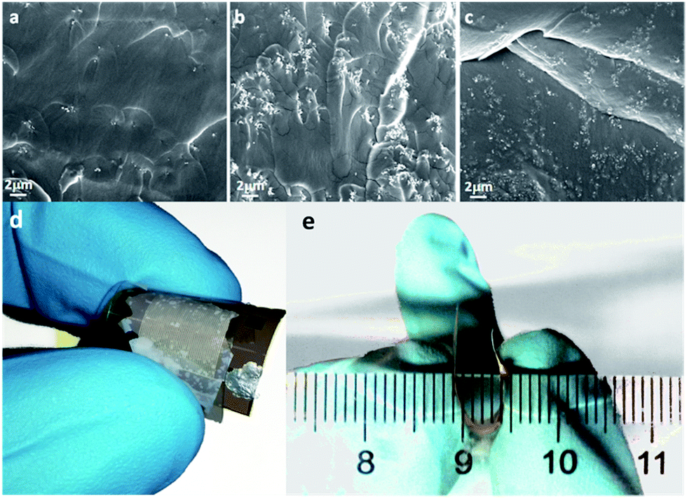 | ||
| Fig. 2 FESEM image of the cross-section of the UV-cured NCs with (a) 1, (b) 5 and (c) 10 phr of ZnO NPs. Optical images of a UV cured BEMA sample including 10 phr ZnO NPs, sandwiched between the Au interdigital electrode lithographed on polyimide and the FTO sputtered electrode on polyester (d); the sample has an irregular shape and is partially transparent, allowing the observation of the tracks and gaps of the interdigital architecture behind. Manual bending of the device, showing that it is easy to realize a curvature radius of 2.5 mm (e). | ||
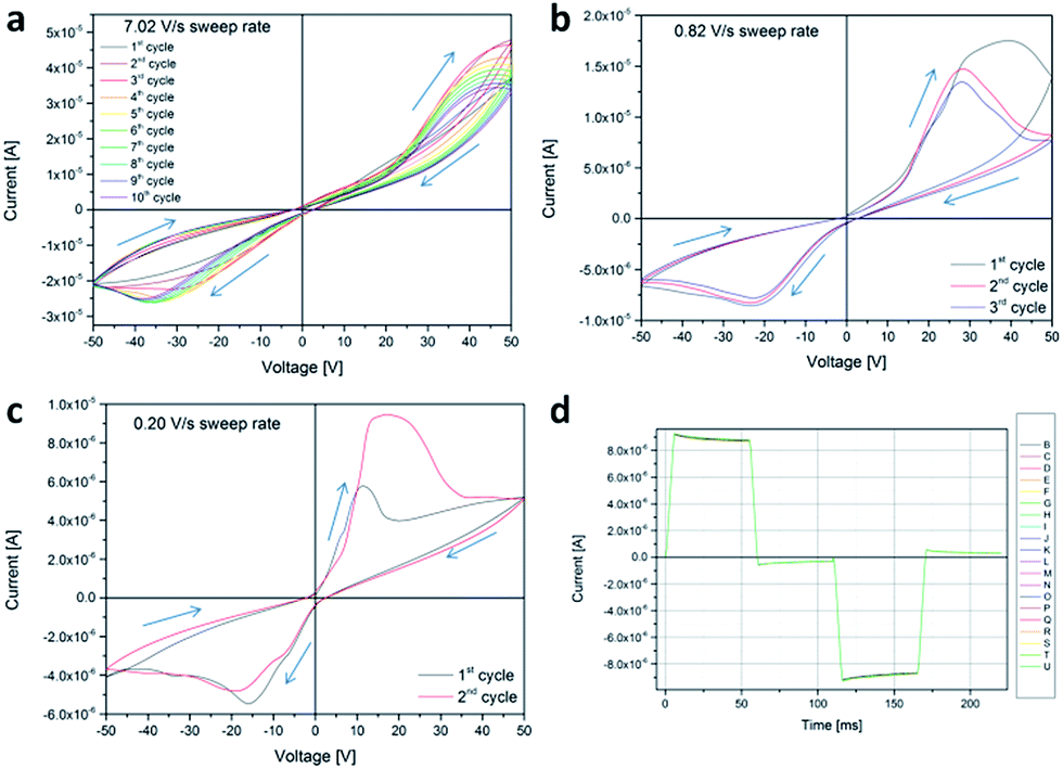 | ||
| Fig. 3 IV cyclic curves of the UV-cured BEMA NCs with 1 phr of ZnO NPs (group 1), at 7.02 V s−1 voltage sweep rate (a), 0.82 V s−1 (b) and 0.20 V s−1 (c). Pulsed cyclic measurements under a trapezoidal waveform (d). Measurements were taken in air at room temperature in CPE configuration, with Au/FTO asymmetric electrodes. | ||
By increasing the amount of ZnO NPs (Fig. 4, panels from a to c) an increase of the NC conductivity and maximum current flowing through the device was observed, in the CPE configuration. The hysteretic response, featuring two distinct levels of resistivity for the down–up and for the up–down cycle, is such that a fast sweep rate produces higher currents via multiple cycling and an “8” shaped butterfly common to memristive devices. By reducing the sweep rate, we recover the same behaviour as previously described. Pulsed measurements always end in a distinguishable idle current of +40 (+395) nA, as seen in Fig. 4d. The same phenomenology is seen analyzing the pure matrix, with a smaller hysteresis and lower currents, featuring a wider hysteresis at low sweep voltages (see Fig. S4†). This may be explained by referring to previous literature, where the bistable resistance is ascribed to charge trapping and space-charge field inhibition of the injection, specifically for MIM structures.42 In our case, the MIM structure is obtained by contacting the pure matrix with the two flexible foils (Au on polyimide and FTO on polyester) from opposite sides. The stability in response is also a function of the ZnO content, as the oscillation between subsequent scans is reduced in amplitude upon increasing the ZnO content. From the linear scale graphs, we may also notice quite a strong asymmetry in the response, which is not dependent on the ZnO content. The electrical asymmetry (ratio between positive and negative area) is easily quantified looking at the energy dissipated per cycle (energy loss), as reported in Table S1.† This feature may be explained as a “gravitational asymmetry” of the samples, having a different distribution of the filler, depending on the parallel (antiparallel) alignment of the normal to the surface and the gravitational acceleration. Using asymmetric Au/FTO plates, the bigger full FTO (smaller lithographed Au) plate was able to polarize a higher (lower) amount of dielectric particles, producing stronger (smaller) dissipation.
 | ||
| Fig. 4 IV cyclic curves of the UV-cured BEMA NCs with 10 phr of ZnO NPs (group 1), at 7.02 V s−1 voltage sweep rate (a), 0.82 V s−1 (b) and 0.20 V s−1 (c). Pulsed cyclic measurements under a trapezoidal waveform (d). Measurements were taken in air at room temperature in the CPE configuration, with Au/FTO asymmetric electrodes. | ||
Measurements taken with symmetrical Cu electrodes are shown in the ESI.† The reproducibility of the response was assessed by repeating measurements over a time span of 12 months of ageing the samples under room conditions, finding no evidence of decay/enhancement of the resistive switching behaviour, as well as no moisture dependency (relative humidity of ambient ranging between 5 and 95%).
Another feature that has to be pointed out, referring to all panels from a to c of both Fig. 3 and 4, is the Negative Differential Resistance (NDR), particularly evident in the third quadrant.
NDR may be explained by referring to a quite recent work, where the charge storage mechanism appears to be still under debate and where another explanation is given, much more interesting and appropriate to our case study.43 In fact, an NDR phenomenon could be produced by an interface insulator layer approaching molecular dimensions. ZnO, as TiO2 and other oxides, is a wide band gap semiconductor, whose conductivity may be enhanced via a reduction process. Normally as-synthesized ZnO materials are n-doped, as a result of some oxygen vacancies in the lattice.44 These vacancies could be seen as points with an accumulation of positive charge.45 In this frame, surface oxygen vacancies could interact with the ether–oxygens of ethylene glycol chains present in the resin since they are nucleophilic moieties.46 These secondary bonds could promote electron transfer between the polymer matrix and ZnO particles and thus enhance the conductivity of the composites since the ZnO conductance is much higher than the matrix one. Furthermore, literature reports on simulations show that oxygen vacancies attract zinc atoms to interstitial sites, thus removing oxygen increases the conductivity of ZnO.47 Actually, the higher the ZnO content, the more the surface is in contact and thus the whole current flow. When the electrical field becomes high enough (above 150 kV m−1 for all the samples) a second process occurs, saturating the current flow between ZnO and the polymer matrix and thus causing an NDR phenomenon. We suppose that this phenomenon produces a weakening of the polymer matrix–ZnO particle interaction that produces as an output an increase of the composite resistance of 2–3 times compared to that of the initial resistance (see Table S1†). Another evidence for a reversible behaviour in ZnO comes from the many reports on gas sensors.48 As an example, hydrogen diffusing through ZnO is thought to be responsible for a resistance decrease, resulting from the reaction between hydrogen and negatively charged oxygen, resulting in the desorption of a water molecule.49 This decreases the overall resistivity of the system, but still remains a reversible phenomenon, completely recovered when the gas is purged (in the sensor case) or the electric field is cycled (in our case).
In commenting another model proposed to explain NDR phenomena and the resistive hysteresis found in hybrid heterostructures comprising ZnO nanorods and poly(methylmethacrylate), based on the switching between a trap-controlled space charge limited conduction (TC-SCLC) and a trap-free space charge limited conduction (TF-SCLC), we oppose the continuity of electrical response that shows no sharp transition (Fig. 3 and 4) and most importantly the inadequacy of the picture of conduction filaments, that cannot develop in the NC systems described here (Fig. 1).50
We also measured a sample under a constant nitrogen flow of 200 sccm at room temperature in order to study the evolution of the electrical response, while molecular oxygen is progressively reduced and then introduced back again (ESI†). Important features are the constant presence of the hysteresis, with a reduction of the cycle area, maintaining the nanobattery characteristics of the system, with a pretty constant open circuit voltage of −1.85 ± 0.15 V (+2.40 ± 0.20 V) and short circuit current of −7 ± 2 nA (+7 ± 4 nA).51
The most remarkable effects are seen under the pulsed waveform (ESI†): the particular setup adopted for having control over gas injection flow resulted in longer wirings exceptionally sensitive to ambient noise, in particular to grid frequency, inducing noise currents several orders of magnitude bigger than signals. Careful filtering techniques were adopted, involving adjacent averaging, Savitzky–Golay polynomials and Fast Fourier Transform (FFT) filtering, through which it was possible to evidence impedance bistability after the programming pulses. Two well separated impedance states, corresponding to −113 (+4) kΩ after positive (negative) pulse, were recorded (ESI†).
Regarding group 2 (BEDA ZnO NP), from the structural point of view the two monomers are both composed by a rigid moiety (bisphenol-A), two lateral flexible chains (ethylene oxide groups) and then two similar reactive groups (methacrylate and acrylate respectively). The most important difference between the monomers is that in BEMA the ethylene-oxide/phenol ratio is 15 while in BEDA it is 2. This means that by substituting BEDA in the initial composition we drastically reduced the presence of ethylene–oxide groups. Reducing the abundancy of ethylene-oxide groups in the composite, by changing the relative ratio between bisphenol-A and lateral ethoxylated moieties, the prevalence of interaction with the ZnO surface was also decreased, affecting its conductivity towards a more insulating behaviour (Fig. 5, panel a).52 This is a further clear indication of the role of ethylene-oxide/ZnO interaction. Upon cycling the current flowing in the NC decreases, as it occurs upon reduction of the sweep rate. Pulsed waveforms induce a response almost completely masked by the grid frequency noise (not shown).
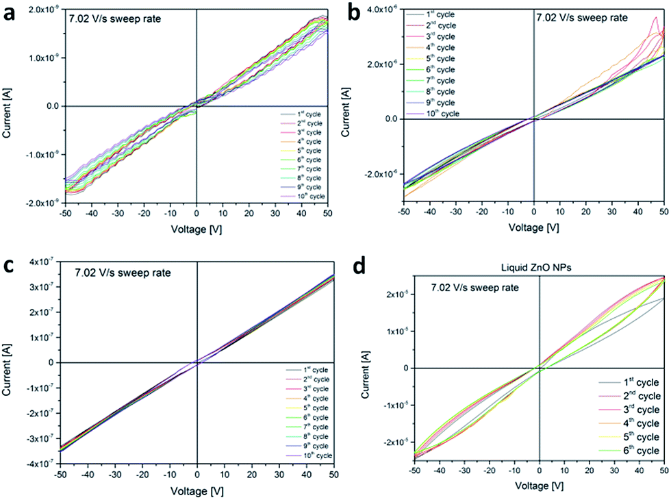 | ||
| Fig. 5 IV cyclic curves of the UV-cured BEDA with 10 phr of ZnO NPs (group 2), at a 7.02 V s−1 voltage sweep rate (a); IV cyclic curves of the UV-cured BEMA composites with 10 phr of ZnO microparticles (group 3), at a 7.02 V s−1 voltage sweep rate (b); IV cyclic curves of the UV-cured BEMA composites with 10 phr of Zn:ZnO NPs (group 4), at a 7.02 V s−1 voltage sweep rate (c); IV cyclic curves of the uncured BEMA monomer with 10 phr of ZnO NPs (group 5, synthetic liquid resistive hysteresis devices), at a 7.02 V s−1 voltage sweep rate (d). Measurements were taken in air at room temperature in the CPE configuration, with Au/FTO asymmetric electrodes. | ||
Other measurements involving blends done at several ratios of BEMA over BEDA, with 5 phr ZnO NPs added, were characterized using Cu symmetric electrodes, are shown in Fig. S5.†
Regarding group 3 (BEMA ZnO μP, Fig. 5b), we observed that the overall conductivity of micro-sized powder based composites is lower than the nano-sized counterpart, in particular the maximum current density sustained by the former (10 phr is ten times smaller than that of the latter, at high sweep rates, and four times at small). Under a pulsed waveform the difference in the two idle states after positive (negative) pulses could be seen. The smaller interaction area between the matrix and filler does not allow efficient charge transfer and thus affects the conductivity, still maintaining the hysteretic behaviour, that is due to the chemistry of the system. Group 3 conduction properties are useful to understand that the resistive hysteresis is driven by chemistry and that the specific surface is helpful for a better engineering of the device.
Group 4, BEMA ZnO:Zn NP, were synthesized in order to check the effect of the presence of p-defects on the electrical properties of the composites. All of the curves (Fig. 5c) showed a vanishingly small hysteretic behaviour if compared with standard nanosized ZnO but also to microsized ZnO, confirming the importance of the chemistry of the system upon interacting with oxygen vacancies. No substantial difference is seen upon reducing the voltage sweep rate. Regarding the pulsed waveforms, a faint signal could be measured by averaging/filtering the grid noise.
Group 5 of samples (BEMAliq ZnO NP) was prepared to further justify our theory regarding ICM; this proof resulted in the realization of the first ever synthetic liquid memristor, in other words the suspension of ZnO NPs in the monomer. Liquid formulations of BEMA monomers containing 10 phr of nanometric ZnO were tested using a direct contact setup with stainless steel blocking electrodes (electrode area 1 cm2, distance between the electrodes 300 μm) performing cyclic measurements in the same range and conditions as above. The formulations were prepared by directly mixing the ZnO powders in the monomers, dispersion was performed by sonication for 30 minutes followed by mechanical high-shear mixing using IKA Ultraturrax (5 min, 10000 rpm). In Fig. 5d IV curves of monomers containing 10 phr of ZnO are reported. It is possible to observe that, differently if compared to cured formulations, the electrical response is only slightly modified by the presence of the ZnO nanopowders. However a certain hysteresis is present, confirming the considerations on the interaction between ethylene–oxide moieties and ZnO surface reported in the main text. The pulsed waveform characterization (ESI†) clearly shows that still is possible to isolate correctly the two resistance states programmed by positive (negative) pulses.
Conclusions
To conclude, the result of the chemical interaction between ethoxylated groups of the polymeric matrix and oxygen vacancies found at the surface of the ZnO fillers is in line with literature results obtained by other research groups, and highlighted and showed the production of a resistive hysteresis in composites containing ZnO and BEMA, allowing also the stable realization of a logic state, read as a current or resistance, programmable through the use of voltage pulses of suitable sign, amplitude and duration. The phenomenology was categorized as an interfacial coupling mechanism, that is under the field of molecular electronics/picoelectronics: its smallest building block, the association between an oxygen vacancy and an ethylene oxide group lying in the hundred of picometers range. Several composite families were studied, changing the surface functionality of the particles, the characteristics of the polymeric matrix, the size of the ZnO particles, the solid/liquid nature of the matrix, the atmosphere and the electrode materials. By controlling the chemistry of the system, the electronic properties of the composites could be modified and thus the conductivity and resistive hysteresis could be tuned.Experimental section
Bisphenol-A ethoxylate dimethacrylate (BEMA, EO/phenol = 15, Mw ∼1500, Aldrich) and bisphenol-A ethoxylate diAcrylate (BEDA, EO/phenol = 2, Mw = 512, Aldrich) were used as photocurable resins. Commercial nanometric Zinc Oxide (ZnO) Nanotek (diameter 40/100 nm, surface area 25 m2 g−1) was purchased from Alfa-Aesar, commercial micrometric Zinc Oxide Reagenplus (μZnO) (diameter < 5 μm, surface area 0.5 m2 g−1) was purchased from Sigma-Aldrich. Irgacure1173 (BASF) and was employed as a photoinitiator (2 phr in each formulation).For ZnO:Zn powders, pure (>99.5%) ZnO powder with a particle size of 0.1–1 μm and granulated Zn powder with a diameter of granules in the range 1–10 μm were used as initial materials. They were weighed in proportions corresponding to the molar composition ZnO:Zn = 10:1. The mechanoactivation treatment of the ZnO:Zn mixture was carried out in ball mills (cylinder volume 5000 cm3, Al2O3 ball diameter 15 mm, total ball mass 1000 g, weighed portion of the specimen under treatment 100 g, rotation speed of the cylinder 60 rpm). Oxygen penetration and Zn oxidation were prevented by vacuum pre-pumping of the cylinder and filling by means of Ar gas to produce a slight excess pressure in the cylinder. The mechanoactivation time was 68 hours. As a result of the mechanoactivation treatment of the ZnO:Zn mixture, we synthesized the ZnO:Zn nanocomposite material composed of ZnO nanocrystallites with dimensions of about 50 nm and less, which were dispersed in an amorphised zinc matrix.
Photocurable formulations were prepared by dispersing different amounts of nanometric ZnO ranging from 1 to 10 phr in BEMA. Dispersion was performed by sonication for 30 minutes followed by mechanical high-shear mixing using IKA Ultraturrax (5 min, 10000 rpm). The photoinitiator was then added in all of the formulations (2 phr). The same procedure was used to prepare the samples containing micro-metric ZnO. For the sample with different matrices, 5 phr of nanometric ZnO were dispersed in a liquid formulation of BEMA/BEDA with different resin weight ratio (100/0, 75/25 and 50/50). The mixtures were then sonicated for 30 minutes and then were mechanically stirred with IKA Ultraturrax (5 min, 10000 rpm). At the end, the photoinitiator was added (2 phr). Liquid formulations were coated on glass slides with a wire wound bar (nominal thickness 100 μm) and then UV-irradiated with a medium pressure Hg bulb (Helios Italquartz, light intensity 70 mW cm−2 measured with EIT UV-meter) for 1 min in a nitrogen inert atmosphere. Free standing, mechanically though films were then detached from the glass slides for further characterization and coupled to flexible electrodes.
DSC analyses were performed using a Netzsch Phoenix 204 F1 apparatus, equipped with a low temperature probe (heating rate: 10 °C min−1). Thermogravimetric analysis (TGA) was performed with a Netzsch TG 209 F1 Libra equipment. Experiments were conducted in air by heating the samples up to 800 °C with a heating rate of 10°C min−1. The gel content was determined on the cured films by measuring the weight loss after 24 h extraction with chloroform at room temperature, according to the standard test method ASTM D2765-84. ATR spectra were collected using a Tensor 27 FTIR Spectrometer (Bruker) equipped with ATR tool. 32 scans were collected with a resolution of 4 cm−1 from 4000 to 400 cm−1. Electrical measurements were performed by using a Keithley-238 High Current Source Measure Unit as the high voltage source and nanoamperometer (samples with symmetrical Cu electrodes), or using a Tektronix-Keithley semiconductor characterization system 4200-SCS (samples with asymmetrical Au/ITO electrodes). In the first case, the electrical properties of the cured films were measured at room temperature in air using a two-point tungsten probe geometry performing cyclic measurements in the range −100/+100 V with 1 V s−1 step, interposing a Cu foil to sandwich the samples in the Cross Point Electrode (CPE) configuration. Each sample had a typical size of 10 × 10 × 0.1 mm, the copper electrodes used for the electrical measurements (data shown in ESI†) were 70 × 70 × 0.1 mm (top) and 10 × 15 × 0.1 mm (bottom).
In the second case, we adopted a full flexible configuration, using on one side Cr/Au coated (20/80 nm respectively, sputtered) 50 μm thick polyimide foil and on the other side FTO coated (250 nm, sputtered) 100 μm thick polyester foil. The Au electrode was optically lithographed with an interdigital geometry, having tracks 100 μm wide separated by a gap of 100 μm; on the contrary the FTO counter electrode was not lithographed. Also in this case the resulting configuration was a CPE with a sandwiched sample. Cyclic measurements were performed both in air and under continuous nitrogen flow (200 sccm) always at room temperature in the range −50/+50 V at three different sweep rates, exploring the whole range technologically available (7.02, 0.82 and 0.20 V s−1). Pulses measurements were such that the sample was submitted to a trapezoidal waveform, with a slew rate of 4 kV s−1, a pulse height of 20 V, a pulse duration of 50 ms and an idle duration of 50 ms. The pulse sequence was: +20 V, idle, −20 V, idle.
Acknowledgements
The authors are grateful to Simone Merlo for his initial studies and experiments. Authors contribution: I. Roppolo and A. Chiolerio contributed substantially and equally to this work. K. Bejtka performed FESEM characterization, A. Asvarov contributed to the discussion and prepared the microparticles, C. F. Pirri contributed to the discussion.Notes and references
- W.-P. Lin, S.-J. Liu, T. Gong, Q. Zhao and W. Huang, Adv. Mater., 2014, 26, 570–606 CrossRef CAS PubMed.
- R. M. Mutiso, J. M. Kikkawa and K. I. Winey, Appl. Phys. Lett., 2013, 103, 223302 CrossRef.
- M. A. Zidan, H. A. H. Fahmy, M. M. Hussain and K. N. Salama, Microelectron. J., 2013, 44, 176–183 CrossRef.
- L. O. Chua, IEEE Trans Circuit Theory, 1971, pp. 507–519, CT-18 Search PubMed.
- D. B. Strukov, G. S. Snider, D. R. Stewart and R. S. Williams, Nature, 2008, 453, 80–83 CrossRef CAS PubMed.
- S. Li, F. Zeng, C. Chen, H. Liu, G. Tang, S. Gao, C. Song, Y. Lin, F. Pan and D. Guo, J. Mater. Chem. C, 2013, 1, 5292–5298 RSC.
- A. Bandyopadhyay, S. Sahu and M. Higuchi, J. Am. Chem. Soc., 2011, 133, 1168–1171 CrossRef CAS PubMed.
- A. Sawa, Mater. Today, 2008, 11, 28–36 CrossRef CAS.
- S. Kim, H. Y. Jeong, S. K. Kim, S. Y. Choi and K. J. Lee, Nano Lett., 2011, 11, 5438–5442 CrossRef CAS PubMed.
- A. Geresdi, M. Csontos, A. Gubicza, A. Halbritter and G. Mihaly, Nanoscale, 2014, 6, 2613–2617 RSC.
- W. Banerjee, X. Xu, H. Liu, H. Lv, Q. Liu, H. Sun, S. Long and M. Liu, IEEE Electron Device Lett., 2015, 36, 333–335 CrossRef CAS.
- S. H. Jo, T. Chang, I. Ebong, B. B. Bhadviya, P. Mazumder and W. Lu, Nano Lett., 2010, 10, 1297–1301 CrossRef CAS PubMed.
- B. Standley, W. Bao, Z. Hang, J. Bruck, N. L. Chun and M. Bockrath, Nano Lett., 2008, 8, 3345–3349 CrossRef CAS PubMed.
- X.-D. Zhuang, Y. Chen, G. Liu, P.-P. Li, C.-X. Zhu, E.-T. Kang, K.-G. Noeh, B. Zhang, J.-H. Zhu and Y.-X. Li, Adv. Mater., 2010, 22, 1731–1735 CrossRef CAS PubMed.
- Y. Chen, G. Liu, C. Wang, W. Zhang, R.-W. Li and L. Wang, Mater. Horiz., 2014, 1, 489–506 RSC.
- U. S. Bhansali, M. A. Khan, D. Cha, M. N. Almadhoun, R. Li, L. Chen, A. Amassian, I. N. Odeh and H. N. Alshareef, ACS Nano, 2013, 7, 10518–10524 CrossRef CAS PubMed.
- J. J. Yang, D. B. Strukov and D. R. Stewart, Nat. Nanotechnol., 2013, 8, 13–24 CrossRef CAS PubMed.
- J. C. Scott and L. D. Bozano, Adv. Mater., 2007, 19, 1452–1463 CrossRef CAS.
- S. L. Lim, Q. Ling, E. Y. H. Teo, C. X. Zhu, D. S. H. Chan, E. T. Kang and K. G. Neoh, Chem. Mater., 2007, 19, 5148–5157 CrossRef CAS.
- B. Hu, F. Zhuge, X. Zhu, S. Peng, X. Chen, L. Pan, Q. Yan and R.-W. Li, J. Mater. Chem., 2012, 22, 520–526 RSC.
- W. J. Joo, T. L. Choi, K. H. Lee and Y. Chung, J. Phys. Chem. B, 2007, 111, 7756–7760 CrossRef CAS PubMed.
- Y.-C. Lai, K. Ohshimizu, W.-Y. Lee, J.-C. Hsu, T. Higashihara, M. Ueda and W.-C. Chen, J. Mater. Chem., 2011, 21, 14502–14508 RSC.
- S.-J. Liu, Z.-H. Lin, Q. Zhao, Y. Ma, H.-F. Shi, M.-D. Yi, Q.-D. Ling, Q.-L. Fan, C.-X. Zhu, E.-T. Kang and W. Huang, Adv. Funct. Mater., 2011, 21, 979–985 CrossRef CAS.
- S. Menzel, E. Linn and R. Waser, Redox-based Resistive Memory, in Emerging Nanoelectronic Devices, John Wiley & Sons, Chichester, UK, 2015 Search PubMed.
- A. Jasmin, S. Porro, A. Chiolerio, C. F. Pirri and C. Ricciardi, Polymer coated ZnO nanowires for memristive devices, Proceedings of the 15th IEEE International Conference on Nanotechnology, Rome, Italy, July 27–30, 2015 Search PubMed.
- F. Raffone, F. Risplendi and G. Cicero, Nano Lett., 2016, 16, 2543–2547 CrossRef CAS PubMed.
- Ü. Özgür, Y. I. Alivov, C. Liu, A. Teke, M. A. Reshchikov, S. Doǧan, V. Avrutin, S. J. Cho and H. Mork
![[o with combining cedilla]](https://www.rsc.org/images/entities/char_006f_0327.gif) , J. Appl. Phys., 2005, 98, 1–103 CrossRef.
, J. Appl. Phys., 2005, 98, 1–103 CrossRef. - Z. R. Tian, J. A. Voigt, J. Liu, B. McKenzie, M. J. McDermott, M. A. Rodriguez, H. Konishi and H. Xu, Nat. Mater., 2003, 2, 821–826 CrossRef CAS PubMed.
- M. Laurenti, D. Perrone, A. Verna, C. F. Pirri and A. Chiolerio, Micromachines, 2015, 6(11), 1729–1744 CrossRef.
- M. Laurenti, A. Verna and A. Chiolerio, ACS Appl. Mater. Interfaces, 2015, 7(44), 24470–24479 CAS.
- S. A. Wilson, R. P. J. Jourdain, Q. Zhang, R. A. Dorey, C. R. Bowen, M. Willander, Q. U. Wahab, S. M. Al-hilli, O. Nur, E. Quandt, C. Johansson, E. Pagounis, M. Kohl, J. Matovic, B. Samel, W. van der Wijngaart, E. W. H. Jager, D. Carlsson, Z. Djinovic, M. Wegener, C. Moldovan, E. Abad, M. Wendlandt, C. Rusu and K. Persson, Mater. Sci. Eng., R, 2007, 56, 1–129 CrossRef.
- J. Park, S. Lee, J. Lee and K. Yong, Adv. Mater., 2013, 25, 6423–6429 CrossRef CAS PubMed.
- C. H. Huang, J. S. Huang, S. M. Lin, W. Y. Chang, J. H. He and Y. L. Chueh, ACS Nano, 2012, 6, 8407–8414 CrossRef CAS PubMed.
- D. I. Son, C. H. You, J. H. Jung and T. W. Kim, Appl. Phys. Lett., 2010, 97, 013304 CrossRef.
- J. Jang, W. Park, K. Cho, H. Song and T. Lee, Curr. Appl. Phys., 2013, 13, 1237–1240 CrossRef.
- M. Laurenti, S. Porro, C. F. Pirri, C. Ricciardi and A. Chiolerio, Crit. Rev. Solid State Mater. Sci., 2016 Search PubMed , accepted for publication.
- A. Chiolerio, I. Roppolo, V. Cauda, M. Crepaldi, S. Bocchini, K. Bejtka, A. Verna and C. F. Pirri, Nano Res., 2015, 8(6), 1956–1963 CrossRef CAS.
- M. Sangermano, I. Roppolo and M. Messori, in Photocured Materials, The Royal Society of Chemistry, 2015, pp. 121–133 Search PubMed.
- A. Chiolerio, I. Roppolo and M. Sangermano, RSC Adv., 2013, 3, 3446–3452 RSC.
- I. Roppolo, E. Celasco, M. Sangermano, A. Garcia, T. Gacoin, J. P. Boilot and S. Perruchas, J. Mater. Chem. C, 2013, 1, 5725–5732 RSC.
- S. P. Pappas and W. Kuhhirt, J. Paint Technol., 1975, 47, 42–48 CAS.
- L. D. Bozano, B. W. Kean, V. R. Deline, J. R. Salem and J. C. Scott, Appl. Phys. Lett., 2004, 84, 607–609 CrossRef CAS.
- Y. Du, H. Pan, S. Wang, T. Wu, Y. P. Feng, J. Pan and A. T. S. Wee, ACS Nano, 2012, 6, 2517–2523 CrossRef CAS PubMed.
- L. Vayssieres, K. Keis, A. Hagfeldt and S. E. Lindquist, Chem. Mater., 2001, 13, 4395–4398 CrossRef CAS.
- A. Janotti and C. G. Van De Walle, Rep. Prog. Phys., 2009, 72, 126501 CrossRef.
- C. Y. Ryu, M. J. Spencer and J. V. Crivello, Macromolecules, 2012, 45, 2233–2241 CrossRef CAS.
- Y. S. Kim and C. H. Park, Phys. Rev. Lett., 2009, 102, 103902 CrossRef PubMed.
- A. Gurlo and R. Riedel, Angew. Chem., Int. Ed., 2007, 46(21), 3826–3848 CrossRef CAS PubMed.
- A. Qurashi, N. Tabet, M. Faiz and T. Yamzaki, Nanoscale Res. Lett., 2009, 4, 948–954 CrossRef CAS PubMed.
- Z. L. Tseng, P. C. Kao, M. F. Shih, H. H. Huang, J. Y. Wang and S. Y. Chu, Appl. Phys. Lett., 2010, 97, 212103 CrossRef.
- I. Valov, E. Linn, S. Tappertzhofen, S. Schmelzer, J. van den Hurk, F. Lentz and R. Waser, Nat. Commun., 2013, 4, 1771 CrossRef CAS PubMed.
- S. H. Lee, S. H. Oh, Y. Ji, J. Kim, R. Kang, D. Khim, S. Lee, J. S. Yeo, N. Lu, M. J. Kim, H. C. Ko, T. W. Kim, Y. Y. Noh and D. Y. Kim, Org. Electron., 2014, 15, 1290–1298 CrossRef CAS.
Footnote |
| † Electronic supplementary information (ESI) available: TGA and DSC thermograms, ATR spectra, and supplementary electrical measurements. See DOI: 10.1039/c6ra10503c |
| This journal is © The Royal Society of Chemistry 2016 |