Two-dimensional CdS intercalated ZnO nanorods: a concise study on interfacial band structure modification
Hind Fadhil Oleiwiae,
Sin Tee Tan c,
Hock Beng Lee
 c,
Chi Chin Yap
 *c,
Riski Titian Ginting
 d,
Azmi Zakaria*b,
Abdelelah Alshanablehc,
Chun Hui Tanc,
Mohammad Hafizuddin Haji Jumali
 c,
Muhammad Yahayac and
Zainal Abidin Talibb
aInstitute of Advanced Technology, Universiti Putra Malaysia, 43400 UPM Serdang, Selangor, Malaysia
bDepartments of Physics, Faculty of Science, Universiti Putra Malaysia, 43400 UPM Serdang, Selangor, Malaysia. E-mail: azmizak@gmail.com
cSchools of Applied Physics, Faculty of Science and Technology, Universiti Kebangsaan Malaysia, 43600 UKM Bangi, Selangor, Malaysia. E-mail: ccyap@ukm.edu.my
dDepartments of Flexible and Printable Electronics, Chonbuk National University, Jeonju 561-756, Republic of Korea
eDepartments of Physics, Faculty of Science for Women, University of Baghdad, Baghdad, Iraq
First published on 18th May 2016
Abstract
The controllable growth of metal sulfide–metal oxide based nanomaterials with a tunable band gap structure is vital in the fabrication of new generation optoelectronic devices. In this paper, two-dimensional hierarchical CdS/ZnO nanorod arrays were successfully grown via a low temperature hydrothermal-SILAR method. A concise mechanism related to the surface and band gap modification on the CdS/ZnO nanorods was investigated under various CdS deposition cycles (N). The diameter and surface roughness properties of the sample were found to be linearly dependent on the value of N. A bathochromic shift in the optical energy band gap revealed the quantum size effects of the CdS/ZnO nanorods, as well as the induced interface band state and energy band split in the ZnO band state. An impressive improvement in the crystallinity of the sample was also observed under the CdS treatment. The correlation between the optical band gap and photovoltaic efficiency was evaluated. The results proved that the ZnO nanorod/CdS devices exhibited a threefold higher power conversion efficiency in comparison to a pristine ZnO nanorod device.
Introduction
Band gap engineering recurrently imparts superior reactivity to semiconductor nanomaterials. The dynamic charge localization and effective dielectric permittivity in oxides have emerged as an area of current study in the modification of the optical and electrical properties of advanced functional nanomaterials.1–3 The intercalation of metal and quantum dot nanoparticles on direct band gap semiconductors such as ZnO has been a sensational discovery in recent years. Considering the constraints of fabrication costs, quantum dots (QDs) such as CdS, PbS and CdSe, with high extinction coefficients, tunable bandgaps and large intrinsic dipole moments are often chosen to improve the electrical properties of devices, especially in boosting the power conversion efficiency (PCE) of inverted organic hybrid solar cells (IOSCs).4–8 The surface interface of metal-inorganic semiconductors have shown strong credentials in enhancing electron extraction during photocurrent generation. In correlation with this, Chu’s group reported on band gap alignment modification in a ZnO nanostructure using an electrochemically active biofilm.9 There are some works reporting that the incorporation of CdS into a metal oxide framework could lead to ultraviolet photoconductivity enhancement.10,11 However, a concise study on band structure modification in interlayer CdS/ZnO nanorod arrays is not yet discussed in most research findings.In our recent work, we are focusing on the interfacial layer surface modification of ZnO nanorods via various kinds of dopant, such as Mg, Ga, Ag and Bi.12–14 It is noteworthy that the doping technique is an alternative way to easily tune the band gap of the semiconductor. To validate the correlation between the band gap alignment and device performance, in the present work, we introduced a facile synthesis method to alter the single band structure to interface induced band gap states by controlling the CdS deposition cycle via successive ionic layer adsorption and reaction (SILAR). The influence of the altered band gap on the PCE of solar cells was also investigated. Our experimental results indicated that a novel bathochromic shift and the presence of CdS optical band energy were linearly dependent on the number of CdS deposition cycles. The disordered interfacial region (CdS coated region) is believed to be one of the main factors which induced the band gap states and promoted the energy band split level in the ZnO material, which later led to the band gap narrowing. Furthermore, a reduction in the optical defect region also played an important role in enhancing the free mobilized electron in the QDs–metal oxide framework that indirectly improved the device performance. The related mechanism is proposed and discussed systematically in this work.
Experimental
Preparation of CdS/ZnO nanorod arrays and device fabrication
Uniformly oriented ZnO nanorod arrays (ZNRs) were successfully prepared on a fluorine tin oxide (FTO) substrate according to a conventional hydrothermal technique.15,16 CdS quantum dots (QDs) were anchored on the surface of ZNRs via a SILAR approach.17 In typical procedures, ZNRs were dipped for 5 minutes for each cycle in both QD aqueous precursor solutions prepared from equimolar 0.05 M cadmium acetate dihydrate (Cd(CH3COO)2·2H2O) and sodium sulfide nonahydrate (Na2S·9H2O) (Sigma Aldrich). The samples were subsequently rinsed with deionized water after each cycle. It is important to note that the two-step procedure reported herein is considered as a single QD deposition cycle. Thereafter, the samples were rinsed with deionized water and ethanol to allow fast drying. Finally, the samples were subjected to a post-heating treatment at 120 °C for 5 minutes. The relationship between the density of CdS on the ZNRs and the number of QD deposition cycles (N) was examined, whereby N = 3, 5 and 7.The donor polymer solution was prepared by dissolving poly(3-hexylthiophene-2,5-diyl) (P3HT, Sigma Aldrich) in chlorobenzene at a concentration of 35 mg ml−1, followed by sonication prior to stirring overnight. The P3HT was spin-coated at 600 rpm for 45 s onto the CdS/ZnO arrays in a humidity controlled glove box, before being spun at 1000 rpm for 60 s for drying. A 100 nm thick Ag electrode with an active area of 0.07 cm2 was deposited onto the active layers using magnetron sputtering.
Characterizations and measurements
The surface morphology of the N-CdS/ZNRs nanostructures were characterized using a field emission scanning electron microscope (FESEM, JEOL JSM-7600F) and a high-resolution transmission electron microscope-electron energy loss spectrometer (HRTEM-EELS, Tecnai F20 TEM Helios-660). Structural properties of the samples were examined by an X-ray diffractometer (XRD, Bruker AXS D8 Advance) under Cu Kα radiation. The thickness of the N-CdS/ZNRs was measured by means of a Veeco Dektak M6 surface profiler. A detailed analysis of the binding energy and chemical compositions of the N-CdS/ZNRs were conducted using an X-ray photoelectron spectrometer (XPS, Kratos/Shimadzu Axis Ultra DLD) operated under a monochromatic Al Kα radiation source at room temperature. Additionally, the optical absorption properties of the samples were obtained using UV-vis-NIR spectroscopy (UV-1650PC Shimadzu). The steady-state photoluminescence (PL) spectroscopy (Edinburgh, FLS920) of the N-CdS/ZNRs and CdS/ZNRs/P3HT films were investigated at an excitation wavelength of 300 nm and 472 nm, respectively.J–V characteristics of the fabricated devices were measured using a Keithley 237 SMU under an illumination of 100 mW cm−2 from a solar simulator with an AM 1.5G filter. Incident photon to electron conversion efficiency (IPCE) spectra were recorded by a Newport IPCE system at a chopping frequency of 10 Hz. Dark charge extraction by linearly increasing voltage (CELIV) technique was performed using a Siglent SDG 1020 function generator (voltage pulse from −0.4 to 3.5 V) and the dynamic response of the mobile carrier extraction was recorded by a digital oscilloscope (Siglent 1103CM) with a Rload-resistance of 50 Ω. For transient photovoltage measurements, the devices were characterized under open circuit conditions under illumination from the solar simulator. A small perturbation of Voc was generated by a pulse from a green collimated light emitting diode (LED) (505 nm, repetition rate = 1 kHz, pulse width = 100 μs). The photovoltage decay was recorded by the aforementioned digital oscilloscope.
Results and discussions
The morphologies of N-CdS/ZNRs were investigated by FESEM, as presented in Fig. 1. Highly oriented crystalline ZNRs were successfully grown on FTO substrates, as presented in Fig. 1A. The average diameter and length of the pristine ZNRs were evaluated via ImageJ software and were found to be (39 ± 2) and (371 ± 3) nm, respectively. Meanwhile, Fig. 1B–D represent FESEM images of N-CdS/ZNRs with N = 3, 5 and 7. Compared to the pristine ZNRs, it was observed that the surface texture of ZNRs became rougher, and the diameter of CdS/ZNRs also increased correspondingly from (61 ± 3) to (67 ± 4) nm with the number of deposition cycles. This observation evidences the successful anchoring of irregular shaped and different sized CdS QDs on the surface of the ZNRs. Additionally, this claim is further supported by the existence of agglomerated CdS QDs between the adjacent nanorods, as shown in the red-circled area (Fig. 1). Instead of modifying the morphology of the ZNRs, it is confirmed that the CdS QDs were successfully deposited on the ZNRs surface.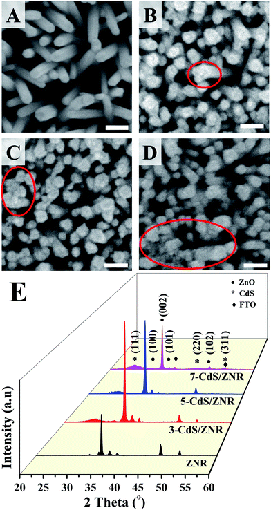 | ||
| Fig. 1 (A–D) FESEM images of N-CdS/ZNRs synthesized via a low-temperature hydrothermal-SILAR method, (E) is the corresponding X-ray diffraction pattern. | ||
The structural properties and purity of the N-CdS/ZNRs were examined via XRD analysis, and the corresponding diffraction patterns are shown in Fig. 1E. All of the diffraction patterns were consistently indexed to the ZnO hexagonal wurtzite structure (JCPDS no file: 36-1451) and the cubic phase of CdS (JCPDS no file: 010-0454), indicating that a combination of crystalline ZnO and CdS formed on the sample. Furthermore, there are no other impurity peaks such as Zn(OH)2 detected in these diffraction patterns. Generally, it was observed that the (002) dominant peak appeared in all of the diffraction patterns, which could be attributed to the c-axis growth orientation of the ZNRs. Noticeably, the intensity of the peak increased after the CdS QDs deposition process. However, the corresponding peaks became weaker when N ≥ 5. Contrarily, the intensity of the (111) peaks of CdS increased linearly with the number of deposition cycles. These results are in good agreement with the aforementioned FESEM discussions, whereby the CdS QDs were successfully intercalated into the ZnO nanostructure. This can be proved by the reduced intensity of the FTO peaks which indicates a higher surface coverage of the CdS QDs on the ZNRs. An in-depth analysis concerning the crystallinity of the sample was carried out by calculating the intensity ratio between the (002) and (101) peaks. Apparently, the ZnO crystallinity of the sample increased from 8.11 to 93.7 as N increased from 3 to 7, manifesting the role of the Cd2+ cation as an oxygen defect reductant in the ZnO crystal framework. To further confirm the chemical composition of the ZNRs and 5-CdS/ZNRs, an EDX point scan was conducted. The results confirm the presence of ZnO in pure ZNRs and 5-CdS/ZNRs with an atomic ratio of 1.26 and 1.08, respectively.
The chemical composition and charge transfer in ZNRs and 5-CdS/ZNRs were further determined by XPS analysis, and the survey spectra are depicted in Fig. 2A. All the presented spectra have been corrected with respect to the element carbon (C) (284.4 eV). Overall, it is confirmed that a pure sample was successfully synthesized in this study, whereby only elemental zinc (Zn), oxygen (O), cadmium (Cd) and sulfur (S) were detected in the spectra. The existence of the element C could arise from atmospheric contamination and the testing conditions.18 A precise analysis was carried out by Gaussian fitting on the narrow scan of the elements Zn, O, Cd and S. For pristine ZNRs (Fig. 2C), the binding energies for Zn 2p3/2 and 2p1/2 were positioned at 1019.7 and 1042.8 eV with a spin-orbital splitting of 23.1 eV, suggesting the presence of Zn2+ in the ZnO crystal structure.19,20 Under the deposition of the CdS QDs on the ZNR surface, both of the peaks were positively shifted (+0.4 eV) to 1020.1 and 1043.2 eV, reflecting the reduced density of valence electrons in the valence band electronic structure of ZnO. This evidence indirectly reflects the interstitial substitution of the element Cd into the Vzn defect site of the ZnO crystal by receiving two valence electrons from oxygen, leading to the formation of a thin layer of CdO and a decrease in the core-hole shielding effects in the Zn electronic state (reduced Zn–O formation). This hypothesis is further supported by the higher electronegativity value in Cd (1.69 eV) compared to Zn (1.65 eV), which increases its tendency to attract valence electrons and form a weak Cd–O bond, or replace the Zn–O–H interactions with Zn–O–Cd. Correspondingly, this phenomenon will change the chemical environment of the surface zinc atoms.21 However, it should be noted that the spin-orbital splitting energy remained constant at 23.1 eV, reflecting that the Cd2+ cation did not change the subatomic structure of Zn. Additionally, the oxygen-related defect states in ZnO and 5-CdS/ZNRs were further analyzed and consistently fitted into two Gaussian peaks centered at 528.5 eV (OI) and 529.6 eV (OII), as presented in Fig. 2B. Basically, OI was attributed to the coulombic attraction between O2− and Zn2+ ions (Zn–O) in the ZnO lattice, while OII was related to oxygen deficient regions, such as areas with high oxygen vacancies.22,23 Fascinatingly, in the case of 5-CdS/ZNRs, it was found that another peak appeared at 531.65 eV, evidencing the presence of Cd–O van der Waals bonding. This result is in good agreement with the aforementioned positive binding energy shift in the Zn element. Moreover, it was noticed that the intensity of the O 1s peaks for 5-CdS/ZNRs was 4 times lower than for the pristine sample. This result infers that the Cd cation behaved as a defect quencher in the ZnO nanorods and indirectly decreased the number of surface trapping sites, which led to a higher efficiency device.11 Additionally, the successive intercalation of CdS nanoparticles on the ZnO nanorods was further proved by the emerging peaks of the elements Cd and S (Fig. 2D and E). It is important to highlight that no binding energy shift occurred in the narrow scan spectra of the elements Cd and S, indicating that a pure CdS compound existed in the sample. To unravel the speculation in CdS formation, a Gaussian fitting was carried on the S spectra. It was found that two peaks were fitted at 159 eV and 161.5 eV, indicating favorable covalent bond formation between Cd and S.
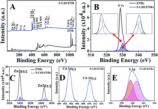 | ||
| Fig. 2 (A) Survey scans for samples of ZNRs and 5-CdS/ZNRs and the corresponding narrow scans for element (B) O, (C) Zn, (D) Cd and (E) S. | ||
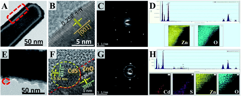
Furthermore, the defect and structural properties of the ZNRs and 5-CdS/ZNRs were investigated by a combined HRTEM-EELS analysis. A clear low magnification TEM image (Fig. 3A) displays a solid ZnO nanorod. The fringe pattern shown in the high resolution image (Fig. 3B) and the clear diffraction spot in selected atomic electron diffraction (SAED) (Fig. 3C) suggest the formation of single crystal ZNRs with an interspace distance of 0.258 nm, which corresponded to the [001] growth direction. The EELS maps in Fig. 3D also show that the nanorods were constructed by the elements Zn and O. This result correlates well with the previous XRD and EDX discussions. On the other hand, under the conditions of CdS QDs surface modification, it can be observed that the CdS QDs with a diameter of 7 nm (bright spot) anchored on the ZNRs surface with an interspace distance of 0.32 nm along the [111] direction (Fig. 3E–G). These results are in good accordance with the EELS mapping, in which the outer decorated nanoparticles have been confirmed as the elements Cd and S, as shown in Fig. 3H.
Apart from this, the optical properties of the ZNRs and N-CdS/ZNRs were measured by UV-vis-NIR spectrometry, and the corresponding spectra are presented in Fig. 4A. For the pristine ZNRs, a single peak was observed at 350 nm, which could be ascribed to near band edge (NBE) absorption of the ZnO semiconductor. Fascinatingly, after CdS surface modification, a new broad peak emerged in the range of 400 to 500 nm, signifying the presence of plasmonic resonance which arises from the CdS QDs. This claim was supported by the similar absorbance spectrum obtained for the pristine CdS sample, as shown in Fig. 4B. Evidently, this peak became more pronounced along with the increase in the number of deposition cycles. This phenomenon can also be confirmed by visual observation (colour changes) of the film’s appearance, whereby the film colour turned from pale to deep yellowish with the increasing number of deposition cycles (Fig. 4A). This indicates a higher density of CdS QDs anchored on the ZNRs surface. Furthermore, the intensity of the NBE peaks also increased with the number of deposition cycles. This observation can be explained by the higher absorptivity of the larger QDs formed under the increase of N. In relation to this, the estimated diameter of QDs was calculated from the Kayanuma and Burus equation24,25 and it was found to increase from 7.44 to 8.31 nm for 5 and 7 cycles, respectively. Additionally, a novel and comprehensive study on optical band gap energy alteration under the influence of CdS deposition cycles was conducted by the Tauc relation26,27 (Fig. 4C). Interestingly, under the simple CdS QDs surface modification, it was noticed that the optical band structure of ZnO was successfully tuned from a single direct band gap to an interface induced band structure, as illustrated in Fig. 4D. In a typical process, it was observed that a bathochromic shift occurred in the NBE peaks from 3.3 to 3.23 eV when N increased to 7. This red-shift phenomenon can be explained by the incorporation of a small amount of Cd2+ cations into the existing point defects (Schottky and Frenkel) that originally formed during the ZnO hydrothermal growth process, simultaneously inducing the split level in the band structure.28 Based on the quantum size effect, it is suggested that a larger QD could further narrow the optical band gap of ZnO (small Eg). Notably, for N ≥ 5, a new interface induced optical band, arising from the dense and ordered layer of CdS QDs, was observed. This novel approach could further reduce the rate of charge recombination in the optoelectronic devices.
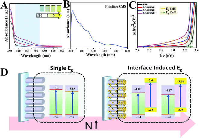 | ||
| Fig. 4 (A) Optical absorbance spectra of N-CdS/ZNRs, (B) pristine CdS, (C) Tauc plot and (D) the illustration in optical energy band gap alteration under the CdS QDs surface modification. | ||
To better understand the role of CdS in the energy band gap alteration and defect engineering in the ZnO nanostructure, steady-state photoluminescence measurements were performed. The corresponding normalized spectrum with respect to NBE emission is displayed in Fig. 5A. All the PL spectra exhibited two main emission peaks, that corresponded to near band edge emission (NBE) and deep level emission (DLE) at 378 and 618 nm, respectively. Generally, an intense NBE peak and a drastic quenching in the intensity of DLE peaks was observed after CdS QDs surface modification. This evidence is in good agreement with the previous XRD and XPS analysis, elucidating the function of the Cd2+ cation in improving the crystallinity of the ZnO crystal structure. For more concise analysis, a deconvolution was conducted via Gaussian fitting in all the PL emission spectra, and the separated regions were denoted as R1, R2, R3 and R4. In particular, R1 is assigned as the near band edge exciton recombination occurring in ZnO. Meanwhile, R2 represents the defects related to zinc interstitials (Zni) whereas R3 arises from oxygen vacancies (Vo) and R4 is commonly reported to originate from oxygen interstitial defects (Oi) and excessive hydroxyl compounds on the ZnO surface.29,30 The area under the intrinsic defect region was significantly suppressed with the increasing number of CdS modification cycles, indicating the successful incorporation of CdS (defect quencher) into the ZnO lattice network. This result is in good accordance with the aforementioned XPS discussion, and the related defect engineering mechanism has been discussed previously with the XPS and XRD data.
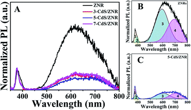 | ||
| Fig. 5 (A) Normalized room temperature PL spectra for N-CdS/ZNRs samples and deconvoluted spectra for (B) ZNRs and (C) 5-CdS/ZNRs. | ||
J–V measurement
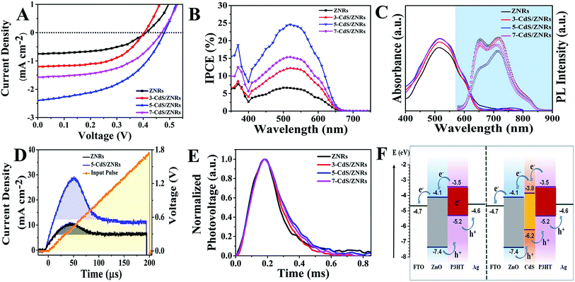
Fig. 6A shows the J–V curves of the N-CdS/ZNRs devices under 100 mW cm−2 illumination. The photovoltaic responses for all of the devices, including the short-circuit current density (Jsc), open-circuit voltage (Voc), fill factor (FF), and power conversion efficiency (PCE) are presented in Table 1. The ZNRs/P3HT device exhibited a Jsc of 0.75 mA cm−2, a Voc of 0.42 V, a FF of 49%, and a PCE of 0.16%. Upon increasing the number of cycles up to 5, both the values of Jsc and Voc gradually increased to 2.58 mA cm−2 and 0.48 V, respectively. As a result, the photovoltaic performance was remarkably improved with a recorded PCE of 0.55%, as shown in Table 1. IPCE measurements were carried out and the spectra are shown in Fig. 6B. In all of the spectra, the sharp peak centered at 370 nm could be ascribed to the photocurrent generated by the ZNRs, whereas the broad peak ranging from 400–650 nm represents the photocurrent contributed by the CdS QDs and P3HT. As expected, the 5-CdS/ZNRs device demonstrated a higher IPCE of up to ∼25% at 520 nm compared to the ZNRs-only device (∼5%). Accordingly, the increasing trend in the IPCE is in good agreement with the Jsc value obtained from J–V measurements (Table 1). However, for the 7-CdS/ZNRs device (larger CdS QD diameter), the PCE dropped to 0.4%, which was mainly due to the decrement of Jsc and Voc, even though the FF improved slightly to 53%. Based on the above results, the photovoltaic performance is highly dependent on the number of CdS QDs deposition cycles.| No. of cycles | Eg (ZnO) (eV) | Eg (CdS QDs) (eV) | Estimated QD diameter (nm) | Voc (V) | Jsc (mA cm−2) | FF (%) | PCE (%) |
|---|---|---|---|---|---|---|---|
| 0 | 3.30 | — | — | 0.42 ± 0.01 | 0.75 ± 0.02 | 49 ± 1 | 0.16 ± 0.14 |
| 3 | 3.27 | — | — | 0.40 ± 0.02 | 1.20 ± 0.03 | 56 ± 1 | 0.27 ± 0.07 |
| 5 | 3.25 | 2.60 | 7.44 | 0.48 ± 0.02 | 2.58 ± 0.02 | 49 ± 1 | 0.55 ± 0.07 |
| 7 | 3.23 | 2.56 | 8.31 | 0.46 ± 0.01 | 1.57 ± 0.05 | 53 ± 1 | 0.40 ± 0.17 |
Fig. 6C shows the absorption and photoluminescence spectra of P3HT coated on ZNRs with various CdS QDs deposition cycles. From the absorption spectra, it can be clearly observed that there was only a slight increase in the visible region, primarily contributed to by the CdS QDs. With the deposition of CdS QDs, the light absorption capability of the photoactive layer was visibly improved, as shown in Fig. 6C, owing to the increase in the scattering cavity at the interface of the CdS QDs and the ZNRs, thus improving the absorption ability of the photoactive layer.31,32 The chemical potential gradient which triggers exciton diffusion to the donor–acceptor was enhanced after the deposition of CdS QDs. This is further supported by the significant PL quenching (Fig. 6C) for 5-CdS/ZNRs coated with P3HT. With the increasing number of cycles of CdS QDs deposition, an intermediate CdS QD energy band was formed between the donor and acceptor interface, which is also commonly known as a cascade band structure. The smaller difference in the lowest unoccupied molecular orbital (LUMO) of P3HT and the conduction band edge CdS QDs intrinsically facilitated charge transport to the electrodes. The cascade structure could assist in reducing the recombination of excitons in the photoactive layer and efficiently dissociate the exciton into free electrons at the CdS QDs/P3HT and ZNRs/CdS QDs interfaces.
In order to validate the improvement of Jsc, dark CELIV measurements were conducted to investigate the equilibrium charge carrier extraction characteristics of the device with different numbers of deposition cycles of CdS QDs (Fig. 6D). Using the well-established equations,33,34 the charge carrier mobility and concentration could be extracted from the CELIV curves. It was found that the charge carrier mobility of the device exhibited an almost 1.4-fold increment from 2.96 × 10⁻⁵ cm2 V−1 s−1 to 4.05 × 10⁻⁵ cm2 V−1 s−1 with 5 cycles of CdS QDs deposition and simultaneously, the charge carrier concentration also improved almost six-fold from 3.37 × 1017 cm−3 to 19.46 × 1017 cm−3. The increase in extracted current could be attributed to the higher density of free charge carriers induced by the CdS QDs layer via the reduction of electron trapping sites such as oxygen vacancies and interstitials.12 As discussed previously, a smaller chemical potential difference between the electronic band structure of CdS QDs and P3HT also enabled rapid charge transport to the electrodes while restricting the bimolecular recombination of charges across the donor–acceptor interface. Therefore, more charges were collected at the electrodes, and this demonstrated the pivotal role of the CdS QDs in the photovoltaic mechanism of the device. For the 7-CdS/ZNRs device, the Jsc and PCE started to reduce drastically owing to three main reasons: (i) the reduced surface density of ZNRs after the erosive deposition of CdS QDs,35 (ii) the impeded interfacial charge transport between the CdS QDs and the ZNRs due to the increasing thickness of the CdS QDs,36 and (iii) the increase of defect sites in the ZNRs due to the superfluous CdS QDs. As a result, the mobility and concentration of the extracted charge carriers were enhanced remarkably, due to the excellent transport properties of CdS QDs.
TPV measurements were carried out to investigate the recombination kinetics of the photo-generated charge carriers in the entire device, and the photovoltage decay curves are shown in Fig. 6E. The carrier recombination lifetime (τ) of each device was extracted from the curves using a single exponential decay function.34 The results revealed that τ increased correspondingly with N from 113 μs (pristine) to 130 and 172 μs (3-CdS/ZNRs and 5-CdS/ZNRs, respectively), but reduced to 159 μs for the 7-CdS/ZNRs device. The changes in τ reflect efficient charge transport after the deposition of CdS QDs, resulting in an increase of Voc. On top of that, the presence of the CdS QDs also served as a recombination barrier by prolonging the diffusion pathway of electrons and holes, simultaneously supporting rapid inter-carrier diffusion between P3HT and the ZNRs. This explained the remarkably longer τ for the CdS QDs coated device up to 5 cycles, which arises from a widening energy band offset between the highest occupied molecular orbital (HOMO) of donors and the LUMO of acceptors. The mechanism is illustrated in Fig. 6F. However, τ was found to decrease at 7 cycles, owing to the larger QD diameter size which indirectly promoted charge trapping sites and hindered the photocurrent injection from the photoactive layer to the ZNRs, which elucidated the shorter τ for 7-CdS/ZNRs compared to the 5-CdS/ZNRs device. Based on the above discussions, even though the energy band offset is larger for ZNRs (for 7 CdS deposition cycles), the larger diameter of the CdS QDs plays a major role in lowering the Voc value.
Conclusion
Uniformly distributed CdS intercalated ZnO nanorod arrays have been successfully grown on an FTO substrate via a low-temperature hydrothermal-SILAR method. The diameter, surface roughness and length of the nanorods were found to be linearly dependent on the number of CdS deposition cycles (N). The Cd2+ cation was found to be an excellent candidate as a defect quencher in the ZnO nanorods, as proved by XRD and PL analysis. Furthermore, a drastic bathochromic phenomenon (red shift) was also observed in the optical energy band gap of ZnO that arose from the presence of the CdS nanoparticles, which generated an interface induced energy band state and increased the energy split in the ZnO band structure. This promising structure was then investigated in the application of IOSCs. Based on the J–V characteristics, it was found that the 5-CdS QDs/ZNRs device exhibited a threefold higher power conversion efficiency in comparison to a pristine ZNR device.Acknowledgements
The authors gratefully acknowledge the financial support for this work from the Fundamental Research Grant Scheme (FRGS) of project No. FRGS/2/2013/SG02/UKM/02/6 and 01-02-13-1345FR. The authors are grateful for the assistance afforded by UKM in various characterizations of samples throughout this work.References
- D. M. Adams, L. Brus, C. E. Chidsey, S. Creager, C. Creutz, C. R. Kagan, P. V. Kamat, M. Lieberman, S. Lindsay and R. A. Marcus, J. Phys. Chem. B, 2003, 107, 6668–6697 CrossRef CAS.
- J. Zhang, W. Lu, Y. S. Li, J. Cai and L. Chen, Acc. Chem. Res., 2015, 48, 1788–1796 CrossRef CAS PubMed.
- A. Alshanableh, C. C. Yap, S. T. Tan, H. B. Lee, C. H. Tan, R. T. Ginting and M. H. H. Jumali, Mater. Lett., 2016, 165, 75–78 CrossRef CAS.
- Y. L. Lee and Y. S. Lo, Adv. Funct. Mater., 2009, 19, 604–609 CrossRef.
- W. J. Beek, M. M. Wienk and R. A. Janssen, Adv. Mater., 2004, 16, 1009–1013 CrossRef CAS.
- L. Wang, D. Zhao, Z. Su and D. Shen, Nanoscale Res. Lett., 2012, 7, 1–6 CrossRef PubMed.
- S. Kilina, D. Kilin and S. Tretiak, Chem. Rev., 2015, 115, 5929–5978 CrossRef CAS PubMed.
- Z. Pan, H. Zhang, K. Cheng, Y. Hou, J. Hua and X. Zhong, ACS Nano, 2012, 6, 3982–3991 CrossRef CAS PubMed.
- S. A. Ansari, M. M. Khan, S. Kalathil, A. Nisar, J. Lee and M. H. Cho, Nanoscale, 2013, 5, 9238–9246 RSC.
- Y. Hao, Y. Cao, B. Sun, Y. Li, Y. Zhang and D. Xu, Sol. Energy Mater. Sol. Cells, 2012, 101, 107–113 CrossRef CAS.
- Q. Cui, C. Liu, F. Wu, W. Yue, Z. Qiu, H. Zhang, F. Gao, W. Shen and M. Wang, J. Phys. Chem. C, 2013, 117, 5626–5637 CAS.
- R. T. Ginting, C. C. Yap, M. Yahaya and M. Mat Salleh, ACS Appl. Mater. Interfaces, 2014, 6, 5308–5318 CAS.
- R. T. Ginting, H. B. Lee, S. T. Tan, C. H. Tan, M. H. B. H. Jumali, C. C. Yap, J.-W. Kang and M. Yahaya, J. Phys. Chem. C, 2016, 120, 771–780 CAS.
- S. T. Tan, A. Ali Umar, A. Balouch, S. Nafisah, M. Yahaya, C. C. Yap, M. Mat Salleh, I. Kityk and M. Oyama, ACS Comb. Sci., 2014, 16, 314–320 CAS.
- T. S. Tee, T. C. Hui, C. W. Yi, Y. C. Chin, A. A. Umar, G. R. Titian, L. H. Beng, L. K. Sing, M. Yahaya and M. M. Salleh, Sens. Actuators, B, 2016, 227, 304–312 CrossRef.
- M. Guo, P. Diao and S. Cai, J. Solid State Chem., 2005, 178, 1864–1873 CrossRef CAS.
- E. Rabinovich and G. Hodes, J. Phys. Chem. C, 2013, 117, 1611–1620 CAS.
- S. Vanalakar, S. Mali, R. Pawar, N. Tarwal, A. Moholkar, J. Kim and P. Patil, J. Appl. Phys., 2012, 112, 044302 CrossRef.
- S. Vanalakar, R. Pawar, M. Suryawanshi, S. Mali, D. Dalavi, A. Moholkar, K. Sim, Y. Kown, J. Kim and P. Patil, Mater. Lett., 2011, 65, 548–551 CrossRef CAS.
- T. Rakshit, S. P. Mondal, I. Manna and S. K. Ray, ACS Appl. Mater. Interfaces, 2012, 4, 6085–6095 CAS.
- W. Cai, G. Duan and Y. Li, Hierarchical Micro/Nanostructured Materials: Fabrication, Properties, and Applications, CRC Press, 2014 Search PubMed.
- S. Sepulveda-Guzman, B. Reeja-Jayan, E. de La Rosa, A. Torres-Castro, V. Gonzalez-Gonzalez and M. Jose-Yacaman, Mater. Chem. Phys., 2009, 115, 172–178 CrossRef CAS.
- N. S. Ramgir, I. S. Mulla and V. K. Pillai, J. Phys. Chem. B, 2006, 110, 3995–4001 CrossRef CAS PubMed.
- E. O. Chukwuocha, M. C. Onyeaju and T. S. Harry, 2012.
- L. Brus, J. Phys. Chem., 1986, 90, 2555–2560 CrossRef CAS.
- H. Li, C. Yao, L. Meng, H. Sun, J. Huang and Q. Gong, Electrochim. Acta, 2013, 108, 45–50 CrossRef CAS.
- M.-M. Bagheri-Mohagheghi, N. Shahtahmasebi, M. Alinejad, A. Youssefi and M. Shokooh-Saremi, Phys. B, 2008, 403, 2431–2437 CrossRef CAS.
- L. Schmidt-Mende and J. L. MacManus-Driscoll, Mater. Today, 2007, 10, 40–48 CrossRef CAS.
- Y.-H. Kim, J.-S. Heo, T.-H. Kim, S. Park, M.-H. Yoon, J. Kim, M. S. Oh, G.-R. Yi, Y.-Y. Noh and S. K. Park, Nature, 2012, 489, 128–132 CrossRef CAS PubMed.
- A. B. Djurišić and Y. H. Leung, Small, 2006, 2, 944–961 CrossRef PubMed.
- C. S. Lao, M.-C. Park, Q. Kuang, Y. Deng, A. K. Sood, D. L. Polla and Z. L. Wang, J. Am. Chem. Soc., 2007, 129, 12096–12097 CrossRef CAS PubMed.
- C. J. Raj, S. Karthick, S. Park, K. Hemalatha, S.-K. Kim, K. Prabakar and H.-J. Kim, J. Power Sources, 2014, 248, 439–446 CrossRef.
- A. Kumar, H.-H. Liao and Y. Yang, Org. Electron., 2009, 10, 1615–1620 CrossRef CAS.
- G. Juška, K. Arlauskas, M. Viliūnas, K. Genevičius, R. Österbacka and H. Stubb, Phys. Rev. B, 2000, 62, R16235 CrossRef.
- Y. Wan, M. Han, L. Yu, J. Jia and G. Yi, RSC Adv., 2015, 5, 78902–78909 RSC.
- G. Chen, J. Seo, C. Yang and P. N. Prasad, Chem. Soc. Rev., 2013, 42, 8304–8338 RSC.
| This journal is © The Royal Society of Chemistry 2016 |

