
Ternary In2S3/In2O3 heterostructures and their cathodoluminescence†
Wenjin Yanga,
Baodan Liu*a,
Yujin Chob,
Bing Yanga,
Benjamin Dierreb,
Takashi Sekiguchib and
Xin Jiang*a
aShenyang National Laboratory for Materials Science (SYNL), Institute of Metal Research (IMR), Chinese Academy of Sciences (CAS), School of Materials Science and Engineering, University of Science and Technology of China, No. 72 Wenhua Road, Shenyang 110016, China. E-mail: baodanliu@hotmail.com; xjiang@imr.ac.cn
bNano-Electronics Materials Unit, National Institute for Materials Science (NIMS), 1-1 Namiki, Tsukuba 305-0044, Japan
First published on 18th May 2016
Abstract
Nanoscale semiconductor heterostructures with superior crystal quality, large surface area and designed interfaces provide more opportunities for building high-performance optoelectronic nanodevices and harvesting clean energy. In this work, we report the rational synthesis of In2S3/In2O3 heterostructures through a two-channel chemical vapor deposition (CVD) process. The In2S3/In2O3 heterostructures feature a bundle-like morphology with In2S3 nanowires covering randomly distributed In2O3 nanoparticles. High-resolution transmission electron microscopy (HRTEM) analysis on the In2S3/In2O3 heterostructures finds that both In2S3 nanowires and In2O3 nanoparticles show a crystalline nature, but the lattice matching between the two crystal domains is not observed at the interface, implying that the heterostructure is formed via a simple physical adsorption. Cathodoluminescence (CL) studies on In2S3/In2O3 heterostructures indicate that the as-synthesized heterostructures have a broad emission in the range of 400–950 nm, covering the whole visible light spectrum from violet to infrared. Finally, the formation process of In2S3/In2O3 heterostructures and their optical emission behaviors are discussed based on detailed structural analyses.
Introduction
Low-dimensional semiconductor heterostructures comprised of cations and/or anions from the same elemental group in neighboring crystal domains have received significant research interest due to their intriguing optoelectronic properties, strong interface effect and multi-functions for specific applications in diverse fields.1–5 Especially, a well-designed interface between different semiconductors or a metal/semiconductor is definitely required to realize an effective separation of photo-generated electrons and holes in a photocatalytic process, with an aim to enhance the internal quantum efficiency (IQE). For instance, Yu et al., Guo et al., and Ni et al. designed ZnS/ZnO heterostructures as a photo-anode for enhanced conversion efficiency for photoelectrochemical applications.6–8 To design a semiconductor heterostructure, two crystal domains from the same elemental group are preferentially considered due to their advantages in lattice-matching and the same/similar crystallographic symmetries.9–13 Based on this principle, numerous binary and ternary semiconductor heterostructures made of different group elements have been created in the past years. Typical examples can be found in Si/Ge,12 InAs/GaAs,13 ZnO/ZnS14 and GaN/AlN15 systems, and large amount of high-performance optoelectronic nanodevices have been developed using such kind of heterostructure nanostructures. Other alternative ways to achieve a heterostructure can also be realized based on the interface lattice-matching rule even though the two crystal domains have different crystallographic symmetries3 or the phase separation from a solid-solution system due to supersaturation, as reported in GaP/ZnS system.16 Recently, we also demonstrate that the defects in 3C–SiC semiconductor nanowires can also induce the preferential nucleation of wurtzite-type GaN (WZ-GaN) to form WZ-GaN/3C–SiC heterostructure nanowires with modified morphology.17As two important In-containing binary semiconductors, In2S3 and In2O3 possess a band-gap of 1.8–2.3 eV and 2.6–3.6 eV, and are widely used as transparent conductive electrodes, fast-response photodetectors and highly-sensitive gas sensors for Cl2, NO2, NH3, H2 and CO detection.18–21 In the past years, extensive efforts have been made in these two binary compounds from rational synthesis to functional device fabrication.22–24 Especially, the optical property characterization and tailoring of In2O3 and In2S3 crystals have attracted tremendous research interests due to their technologically important applications in the field of photovoltaic and optoelectronic devices.22,25–27 However, the combination of In2O3 and In2S3 to form a heterostructure and the investigations on their related structural and optical properties are rarely studied. To our best knowledge, Yang et al. and Tien et al. reported the fabrication of type-I In2O3–In2S3 core–shell nanorods and type-II α-In2S3/In2O3 nanowire heterostructures through a hydrothermal process;28,29 Lee et al. fabricated the In2S3/In2O3 heterojunctions inserted with layered single-walled carbon nanotubes;30 Hara et al. and Sirimanne et al. investigated the nanocrystalline In2S3/In2O3 electrode through sulfurizing In2O3 in H2S atmosphere;31,32 and Xu et al. developed the In2O3/In2S3/Ag nanocubes for photoelectrochemical water splitting.33 Unfortunately, detailed analysis on the phase interface between In2S3 and In2O3 crystal domains and their optical behavior are still in demanding, which is essential to understand the formation process behind the heterostructures.
In this work, we demonstrated the rational synthesis of In2S3/In2O3 heterostructure through a well-designed two-channel chemical vapor deposition (CVD) process proposed in our previous work.34 It is found that the In2S3/In2O3 heterostructures prefer to form bundle-like morphology with In2S3 phase as the trunk nanowires and In2O3 nanoparticles as decorations. The interface between In2S3 and In2O3 crystal domains are further investigated and confirmed by spatially resolved energy-dispersive X-ray spectroscopy (EDS) and high-resolution transmission electron microscopy (HRTEM) techniques. Optical characterizations using cathodeluminescence (CL) measurement confirmed that separated emission bands originating from In2S3/In2O3 heterostructures are observed in the wide range from 400–950 nm. It is supposed that the phase interface and structure defects may have a significant influence on the optical emissions.
Experiment section
Growth of In2S3/In2O3 heterostructures
The In2S3/In2O3 heterostructure nanomaterials are synthesized on Si(111) substrate through a two-channel CVD approach.34 High purity InP slices (Alfa Aesar A Johnson Matthey Company, 99.9999%) and ZnS powder (Sinopharm Chemical Reagent Co., Ltd, AR) are employed as raw reactants to provide In and S sources, respectively. In a typical experiment, the InP and ZnS powders are placed in two separated quartz tubes and flowing Ar gas with a flowing rate of 150 standard cubic centimeter per minute (sccm) is used as the carrier gas. The schematic diagram of the experimental setup is illustrated in ESI Fig. S1.† The growth reaction is fixed at 1375 K for 80 min based on our experience in previous work.Structure and optical property characterizations
The morphology of In2S3/In2O3 heterostructure nanomaterials is characterized by a field emission scanning electron microscopy (FE-SEM INSPECT F50) operating at 20 kV. X-ray powder diffraction (XRD, Bruke D2 PHASER) based on Cu Kα radiation (λ = 1.5418 Å) and high-resolution emission transmission electron microscopy (HRTEM, Tecnai G2 F20) with an accelerating voltage of 200 kV are used to analyze the phases, microstructures and crystal domain boundaries of the nanostructures. Chemical composition is measured by an X-ray energy dispersive spectrometer (EDS) attached on the TEM. Room-temperature cathodoluminescence spectrum of In2S3/In2O3 heterostructure is recorded in an field-emission scanning electron microscope (FE-SEM, Hitachi-S4300) equipped with a CL system (Horiba-MP32S/N) under an accelerating voltage of 5 kV and a beam current of 1000 pA.35Results and discussion
Fig. 1a–c show the typical morphology of In2S3/In2O3 heterostructure nanostructures deposited on a Si substrate. An obvious bundle-like morphology can be observed, which consists of trunk nanowires and side nanoparticles. The bundles have an average dimensional size with a length of 12 μm and a diameter of 0.5–1 μm (ESI, Fig. S5†). Magnified SEM image (Fig. 1b) and TEM image (Fig. 2a) reveal that the bundles are consisted of dozens of thin nanowires with a diameter about 100 nm and large amount of nanoparticles with diameters of 40–50 nm. The aggregation of these thin nanowires to form the bundle trunks can be regarded as a self-assembling process and the decoration of nanoparticles on the surface of nanowires is also at random. Series of growth experiments find that the dimensional size of these In2S3/In2O3 heterostructure nanostructures is strongly dependent on the temperature gradient in the reactor. Slightly reducing the distance between substrate and precursors will lead to a drastic increase of the nanowire and nanoparticle in size, (ESI, Fig. S2†), indicating a faster crystallization rate. Further observation on the nanoparticles shows that these nanoparticles feature a typical octahedron shape (ESI, Fig. S2†), agreeing well with the typical appearance of In2O3 nanostructures reported in previous works.36–38 Preliminary composition analysis on the heterostructure bundles verifies the existence of In, O and S elements (Fig. 2c). However, the back-scattered electron image (BSE, Fig. 1c) shows less difference between the nanowires and nanoparticles due to the approximate relative atomic mass of In2S3 and In2O3. | ||
| Fig. 1 (a) Low-magnification SEM image of In2S3/In2O3 heterostructure nanomaterials; (b and c) magnified SEM image and BSE image of In2S3/In2O3 heterostructures, respectively; (d) XRD pattern of as-synthesized sample and standard XRD data of cubic In2S3 and In2O3; (e and f) crystal unit cells of cubic In2S3 and In2O3, respectively. | ||
 | ||
| Fig. 2 (a) TEM image of as-prepared In2S3/In2O3 heterostructures; inset shows a single In2S3 nanowire with In2O3 nanoparticle; (b and c) EDS spectra collected from the local areas labeled in (a); (d) STEM image of In2S3/In2O3 heterostructure; (e and f) line-scan composition profiles taken along radial and axial directions of In2S3/In2O3 heterostructure in (d), respectively; (g) STEM image and its corresponding EDS elemental mapping of In, S, O elements in a single nanowire. | ||
The designed formation of In2S3/In2O3 heterostructures starts from the original precursors InP and ZnS powders, which comprise of In, P, Zn and S elements and can provide numerous of possibilities for the formation of diverse binary, ternary or quaternary compounds like solid-solutions or heterostructures (In2S3, In2O3, ZnS, ZnO, ZnP, InP, (Zn, In)S, (Zn, In)O, Zn(S, O), In(S, O), (Zn, In)(S, P)).34,39 Therefore, it is definitely essential to examine their composition and phase purity of the as-synthesized nanostructures. Fig. 1d shows the XRD pattern of the nanostructures. The peaks centered at 2θ = 14.2°, 23.4°, 27.5°, 28.7°, 33.3°, 43.7°, 47.8°, and 55.8° can be indexed to the (111), (220), (311), (222), (400), (511), (440), and (533) planes of cubic In2S3 (JCPDS no. 65-0459), while these peaks with 2θ = 21.1°, 30.5°, 35.4°, 37.6°, 50.9°, and 55.8° correspond well to the (211), (222), (400), (411), (440), and (611) planes of cubic In2O3 (JCPDS no. 65-3170). The peak centered at 2θ = 41.6° arises from the Si substrate and 2θ = 20.5° is assigned to SiO2 because of the oxidation of silicon substrate at high temperature. The appearance of In2S3 and In2O3 peaks implies the co-existence of both phases in the form of separated crystal grains or heterostructures. The bright field (BF) and dark field (DF) TEM images further demonstrate the heterostructure feature of In2S3/In2O3 with obvious boundary (ESI, Fig. S3†).
From above analyses, the In2S3/In2O3 heterostructure can be confirmed. However, it is still required to define the exact composition of different crystal domains (the bundles and the octahedral nanoparticles) in local regions. The composition measurement performed on the heterostructure concludes that it is made of In, S and O elements which originate from the In2S3/In2O3 samples, while the detected Cu signal is ascribed to the Cu TEM grid. Further composition analysis using EDS in point mode confirms that both the central thin nanowires and edge nanoparticles share the same In element. In addition, the nanowire portion shows a strong peak intensity of S element rather than O element and the In/S atomic ratio approaches to the stoichiometric value of In2S3, suggesting that the thin nanowires are actually In2S3 phase. Meanwhile, the edge octahedral nanoparticles with regular geometrical shapes exhibit obvious signal intensity in O element and the In/O atomic ratio also matches well with In2O3.36,37 The line-scan composition profiles taken along the radial and axial directions, as well as spatial resolved elemental mapping (shown in the Fig. 2e–g), further verify the spatial distributions of each elements and prove the heterostructures nature of In2O3/In2S3. O signal collected in nanowires suggests that some adsorbed oxygen or doped oxygen exist in In2S3 nanowires. Some impurities related to Zn and P with weak peak intensity can also be detected due to the inevitable contamination from the starting precursors (ESI, Fig. S4†). These results are also in good accordance with the structure and phase data measured by XRD and BSE shown in Fig. 1.
For semiconductor heterostructures, the interface plays a key role in governing the optoelectronic properties such as photocatalytic and photoelectrochemical performance. The sharpness and atomic arrangement at the grain boundary will strongly affect the electrical transport and the migration of electrons, photo-generated electrons and holes, and phonons.30,40,41 Therefore, it is of great significant to understand how the In2S3 nanowires combine with In2O3 nanoparticles. Fig. 3a shows a typical TEM image of In2S3 nanowire bundles decorated with octahedral In2O3 nanoparticles. Unlike most nanowire/nanoparticle heterostructures, it is found that the In2O3 nanoparticles randomly cover on the surface of trunk nanowires and no preferential/regular distribution of the particles is observed. To examine the crystallinity of both In2S3 nanowires and In2O3 nanoparticles, HRTEM analyses performed on individual nanoparticle and nanowire edge (Fig. 3a) are carried out, and their corresponding atomic lattice images are presented in Fig. 3b and c. Apparently, both In2S3 nanowires and In2O3 nanoparticles are well-crystallized with obvious single crystal nature. The HRTEM image shown in Fig. 3b and its corresponding fast Fourier transformation (FFT) with succinct diffraction spots verify that the bundled nanowires are In2S3 with a cubic structure and a space group of Fd![[3 with combining macron]](https://www.rsc.org/images/entities/char_0033_0304.gif) m. The distance of 0.38 nm between adjacent lattice planes matches well with the d-spacing of (220) plane in cubic In2S3 (ESI, Table S1†). Similarly, the nanoparticles can be confirmed to be cubic In2O3 with a space group of Ia (shown in Fig. 3c) and the inter-planar distance of 0.34 nm can be attributed to the d-spacing of (220) plane in cubic In2O3 (ESI, Table S1†). As is known to all, the two materials have the same structure (cubic structure) and very close lattice constants (10.774 Å for In2S3 and 10.140 Å for In2O3), it is plausible to assume that In2S3 and In2O3 may have an epitaxial relationship in lattice-matching. However, carefully observing the In2S3/In2O3 interface using HRTEM does not find obvious epitaxial relationship even though In2S3 and In2O3 have the similar crystallographic symmetry and close lattice parameters (Fig. 3b–e). The difference of space group and atomic configuration of In2O3 and In2S3 crystals (Fig. 1e and f) makes them quite difficult to form epitaxial growth at their phase boundaries. One can see that the protruding In2O3 nanoparticles with octahedral tip have a good crystalline lattice image, whereas the atomic arrangement in the In2S3 area shows a poor crystallization (Fig. 3e). Therefore, it can be found that the decoration of In2O3 nanoparticles on the surface of In2S3 nanowires to form In2S3/In2O3 heterostructures is mainly realized through a self-assemble physical contact rather than epitaxial nucleation. This assertion can be further supported by the random distribution of numerous In2O3 nanoparticles. Interestingly, the thin In2S3 nanowires prefer to assemble together to present bundle-like morphology. It is believed that such tight aggregation is beneficial to the stabilization of In2S3/In2O3 heterostructures based on the principle of surface energy minimization, as observed in WO3/Ag heterostructures.42
m. The distance of 0.38 nm between adjacent lattice planes matches well with the d-spacing of (220) plane in cubic In2S3 (ESI, Table S1†). Similarly, the nanoparticles can be confirmed to be cubic In2O3 with a space group of Ia (shown in Fig. 3c) and the inter-planar distance of 0.34 nm can be attributed to the d-spacing of (220) plane in cubic In2O3 (ESI, Table S1†). As is known to all, the two materials have the same structure (cubic structure) and very close lattice constants (10.774 Å for In2S3 and 10.140 Å for In2O3), it is plausible to assume that In2S3 and In2O3 may have an epitaxial relationship in lattice-matching. However, carefully observing the In2S3/In2O3 interface using HRTEM does not find obvious epitaxial relationship even though In2S3 and In2O3 have the similar crystallographic symmetry and close lattice parameters (Fig. 3b–e). The difference of space group and atomic configuration of In2O3 and In2S3 crystals (Fig. 1e and f) makes them quite difficult to form epitaxial growth at their phase boundaries. One can see that the protruding In2O3 nanoparticles with octahedral tip have a good crystalline lattice image, whereas the atomic arrangement in the In2S3 area shows a poor crystallization (Fig. 3e). Therefore, it can be found that the decoration of In2O3 nanoparticles on the surface of In2S3 nanowires to form In2S3/In2O3 heterostructures is mainly realized through a self-assemble physical contact rather than epitaxial nucleation. This assertion can be further supported by the random distribution of numerous In2O3 nanoparticles. Interestingly, the thin In2S3 nanowires prefer to assemble together to present bundle-like morphology. It is believed that such tight aggregation is beneficial to the stabilization of In2S3/In2O3 heterostructures based on the principle of surface energy minimization, as observed in WO3/Ag heterostructures.42
 | ||
| Fig. 3 (a) TEM images of In2S3/In2O3 heterostructure bundles; (b and c) HRTEM images of nanowire and nanoparticle indicated in (a), respectively; (d) TEM image of a single heterostructure product; (e) HRTEM image corresponding to the region marked in (d). | ||
To disclose the formation of In2S3/In2O3 heterostructures, a tentative growth model is schematically illustrated to describe the possible nucleation and crystallization processes, as shown in Fig. 4. First, InP and ZnS reactants will be decomposed into the elemental precursors in the form of sublimated In, P, Zn and S atoms under high temperature (stage I). Second, these active atoms will be reorganized to nucleate on the Si surface and evolve into one dimensional In2S3 nanowires and In2O3 nanoparticles (stage II). It should be mentioned that the O source in In2O3 nanoparticles comes from the residual O2 in the reaction chamber. Finally, the In2S3 nanowires decorated with In2O3 nanoparticles will be assembled into heterostructure bundles (stage III). Here the wire-like appearance of In2S3 crystal domain and the octahedral shape of In2O3 nanoparticles can be attributed to their own growth nature. Generally, the In2S3 nanowires are commonly found in the CVD process under a high temperature, as reported in previous works.43,44 For In2O3 crystal domain, it has been reported that the In precursor type has a significant influence on its morphology. For example, octahedral nano/micro-particles are usually observed when pure In is used as the raw reactant, while In2O3 nanowires are often obtained with In2O3 powder as precursor and the higher reaction temperature from 1225 K to 1575 K will lead to the size reduction of In2O3 octahedrons from 1 μm to 100 nm.36 The shape of In2O3 nanoparticles is greatly influenced by the surface energy of different planes and the growth rates of each crystallographic facet. It has been reported that the geometrical shape of In2O3 nanoparticles is strongly dependent on the ratio of v{100}/v{111}.45 Hence, the appearance of In2S3 nanowires and In2O3 octahedral nanoparticles are the integration function of thermodynamics and kinetics, while more than just only kinetics or thermodynamics effects. It should be mentioned that the absence of Zn and P elements in the In2S3/In2O3 heterostructures is possibly due to the faster diffusion rate of Zn and P precursors at high temperature, as observed in GaP–ZnSe and (GaN)1−x(ZnO)x pseudobinary solid-solutions.34,46
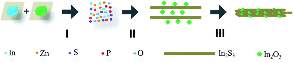 | ||
| Fig. 4 The schematic diagram describing the formation process of In2S3/In2O3 heterostructures. | ||
As two important semiconductors, cubic In2S3 and In2O3 crystals have a band-gap of 1.8–2.3 eV and 2.6–3.6 eV, respectively, corresponding to an emission wavelength in the range of 539–689 nm and 344–476 nm.25,28,47–49 The combination of In2S3 and In2O3 phases will undoubtedly broaden the emission wavelength from violet to visible light, which enables a wider optical emission for efficient photocatalytic applications. To study the optical properties of semiconductor nanostructures, cathodoluminescence technology with high-resolution of wavelength in nano-scale area has been demonstrated to be quite useful and reliable.46,50–53 Fig. 5 shows the CL spectrum collected from the In2S3/In2O3 heterostructure samples under an accelerated voltage of 5 kV and a beam current of 1000 pA. A broad emission band covering the whole visible range can be observed. The CL spectrum can be further divided into three separated bands with typical peaks centered at 482 nm, 645 nm and 800 nm by the Gaussians deconvolution function. Obviously, the emission band with a peak wavelength centered at 645 nm shows the strongest intensity and matches well with the luminescence data of In2S3 crystal. Therefore, it can be concluded that the 645 nm emission should originate from the In2S3 nanowires. The strong luminescence intensity of 645 nm emission is also in good agreement with the predominant In2S3 phase in the heterostructures. The left shoulder with a peak wavelength located at 482 nm can be assigned to the cubic In2O3 phase, even though the 482 nm green emission has been ascribed to the deep trap states or defects in In2S3 nanowires.48 The broad emission band with a peak wavelength centered at 800 nm can be regarded as defect-related luminescence since some structural defects like phase boundary and vacancies are involved in the heterostructure crystals. It has been reported that nitrogen doping in In2O3 nanostructures can also induce a red-light emission at 740 nm.54,55 Previous studies also pointed out that high-density oxygen vacancies in In2O3 nanostructures can also lead to a strong visible light emission due to the recombination of donor band (oxygen vacancy, VO) and acceptor band (indium vacancy, VIn).26,55–57
 | ||
| Fig. 5 Room-temperature CL spectrum of In2S3/In2O3 heterostructures collected under an accelerated voltage of 5 kV and a beam current of 1000 pA. | ||
From above results, it can be seen that the In2S3/In2O3 heterostructures synthesized from a CVD process have predominant merits in crystal quality, large surface areas and phase interfaces, as well as a broad emission band covering from violet to the infrared region, which paves a solid way for efficient visible light absorption and carrier separation towards photocatalytic applications in hydrogen clean energy harvesting and organic solution photodegradation.28,29 Based on current work and the crystallographic characteristics of In2O3 and In2S3 crystals, the rational growth of In2S3/In2O3 heterostructures with sharp interface, tunable emission wavelength and controllable heterostructure configuration (core–shell or hierarchical structure) can be further achieved through careful design and precise control of the nucleation and crystallization process. In this way, the In2S3/In2O3 heterostructure with excellent crystal quality and optical properties will open up more opportunities in the field of optoelectronic nanodevices, clean energy and environment processing.
Conclusions
In summary, ternary In2S3/In2O3 heterostructure nanostructures comprised of In2S3 nanowire bundles and In2O3 octahedral nanoparticles have been fabricated through a two-channel CVD process. Both In2O3 and In2S3 domains exhibit superior crystal quality without obvious structural defects such as stacking faults and twins. However, the lattice matching and the sharp interface in In2O3/In2S3 boundary are not observed due to the self-assembled decoration of In2O3 nanoparticles on the surface of In2S3 nanowires. Room-temperature cathodoluminescence measurement indicates that the In2S3/In2O3 heterostructures show a broad emission band covering from the violet to infrared region, which holds great promise for efficient visible light absorption toward enhanced photocatalytic applications in the field of clean energy harvesting and the photodegradation of organic pollutants.Acknowledgements
This work was partially supported by the Knowledge Innovation Program of Institute of Metal Research with grants No. Y2NCA111A1 and Y3NCA111A1, and the Youth Innovation Promotion Association, Chinese Academy of Sciences (Grant No. Y4NC711171).References
- L. J. Lauhon, et al., Epitaxial core–shell and core–multishell nanowire heterostructures, Nature, 2002, 420(7), 57–61 CrossRef CAS PubMed.
- Y. Wu, et al., Single-crystal metallic nanowires and metal/semiconductor nanowire heterostructures, Nature, 2004, 430(1), 61–65 CrossRef CAS PubMed.
- J. Hu, et al., Epitaxial heterostructures: side-to-side Si–ZnS, Si–ZnSe biaxial nanowires, and sandwich like ZnS–Si–ZnS triaxial nanowires, J. Am. Chem. Soc., 2003, 125(37), 11306–11313 CrossRef CAS PubMed.
- G. Shen, et al., Structure and cathodoluminescence of hierarchical Zn3P2/ZnS nanotube/nanowire heterostructures, Appl. Phys. Lett., 2007, 90(7), 073115 CrossRef.
- B. D. Liu, et al., Synthesis of GaP nanowires with Ga2O3 coating, Appl. Phys. A: Mater. Sci. Process., 2004, 80(7), 1585–1588 CrossRef.
- X.-L. Yu, et al., ZnS/ZnO Heteronanostructure as Photoanode to Enhance the Conversion Efficiency of Dye-Sensitized Solar Cells, J. Phys. Chem. C, 2010, 114(5), 2380–2384 CAS.
- P. Guo, et al., ZnS/ZnO heterojunction as photoelectrode: Type H band alignment towards enhanced photoelectrochemical performance, Int. J. Hydrogen Energy, 2013, 38(29), 13097–13103 CrossRef CAS.
- Y. Ni, et al., Fabrication, Characterization and Properties of Flowerlike ZnS–ZnO Heterogeneous Microstructures Built Up by ZnS-Particle-Strewn ZnO Microrods, J. Phys. Chem. C, 2008, 112(22), 8200–8205 CAS.
- R. Wang and W. Liu, Synthesis and characterization of ZnS tetrapods and ZnO/ZnS heterostructures, Thin Solid Films, 2012, 522, 40–44 CrossRef CAS.
- W. Liu, R. Wang and N. Wang, From ZnS nanobelts to ZnO/ZnS heterostructures: Microscopy analysis and their tunable optical property, Appl. Phys. Lett., 2010, 97(4), 041916 CrossRef.
- P. Guo, et al., Semiconductor alloy nanoribbon lateral heterostructures for high-performance photodetectors, Adv. Mater., 2014, 26(18), 2844–2849 CrossRef CAS PubMed.
- J. Xiang, et al., Ge/Si nanowire heterostructures as high-performance field-effect transistors, Nature, 2006, 441(7092), 489–493 CrossRef CAS PubMed.
- D. Scarpellini, et al., InAs/GaAs Sharply Defined Axial Heterostructures in Self-Assisted Nanowires, Nano Lett., 2015, 15(6), 3677–3683 CrossRef CAS PubMed.
- W. Tian, et al., Flexible ultraviolet photodetectors with broad photoresponse based on branched ZnS–ZnO heterostructure nanofilms, Adv. Mater., 2014, 26(19), 3088–3093 CrossRef CAS PubMed.
- S. D. Carnevale, et al., Three-dimensional GaN/AlN nanowire heterostructures by separating nucleation and growth processes, Nano Lett., 2011, 11(2), 866–871 CrossRef CAS PubMed.
- B. Liu, et al., Solid Solution, Phase Separation, and Cathodoluminescence of GaP–ZnS Nanostructures, ACS Appl. Mater. Interfaces, 2013, 5(18), 9199–9204 CAS.
- B. Liu, et al., Defect-Induced Nucleation and Epitaxy: A New Strategy toward the Rational Synthesis of WZ-GaN/3C–SiC Core–Shell Heterostructures, Nano Lett., 2015, 15(12), 7837–7846 CrossRef CAS PubMed.
- C. Li, et al., In2O3 nanowires as chemical sensors, Appl. Phys. Lett., 2003, 82(10), 1613 CrossRef CAS.
- D. H. Zhang, et al., Detection of NO2 down to ppb levels using individual and multiple In2O3 nanowire devices, Nano Lett., 2004, 4(10), 1919–1924 CrossRef CAS.
- C. Li, et al., Complementary detection of prostate-specific antigen using In2O3 nanowires and carbon nanotubes, J. Am. Chem. Soc., 2005, 127(36), 12484–12485 CrossRef CAS PubMed.
- C. G. Granqvist and A. Hultaker, Transparent and conducting ITO films: new developments and applications, Thin Solid Films, 2002, 411(1), 1–5 CrossRef CAS.
- C. H. Liang, et al., Catalytic growth of semiconducting In2O3 nanofibers, Adv. Mater., 2001, 13(17), 1330–1333 CrossRef CAS.
- K. H. Park, K. Jang and S. U. Son, Synthesis, optical properties, and self-assembly of ultrathin hexagonal In2S3 nanoplates, Angew. Chem., Int. Ed. Engl., 2006, 45(28), 4608–4612 CrossRef CAS PubMed.
- C. H. Lee, et al., Ambient pressure syntheses of size-controlled corundum-type In2O3 nanocubes, J. Am. Chem. Soc., 2006, 128(29), 9326–9327 CrossRef CAS PubMed.
- H. Zhu, et al., Nanoporous In2O3 Nanocrystal Clusters: One-Step Synthesis, Thermal Stability and Optical Property, J. Phys. Chem. C, 2008, 112(12), 4486–4491 CAS.
- M. J. Zheng, et al., Ordered indium-oxide nanowire arrays and their photoluminescence properties, Appl. Phys. Lett., 2001, 79(6), 839 CrossRef CAS.
- L.-Y. Chen, Z.-D. Zhang and W.-Z. Wang, Self-Assembled Porous 3D Flowerlike β-In2S3 Structures:
![[thin space (1/6-em)]](https://www.rsc.org/images/entities/char_2009.gif) Synthesis, Characterization, and Optical Properties, J. Phys. Chem. C, 2008, 112(11), 4117–4123 CAS.
Synthesis, Characterization, and Optical Properties, J. Phys. Chem. C, 2008, 112(11), 4117–4123 CAS. - X. Yang, et al., Synthesis of In2O3–In2S3 core–shell nanorods with inverted type-I structure for photocatalytic H2 generation, Phys. Chem. Chem. Phys., 2013, 15(30), 12688–12693 RSC.
- L.-C. Tien and J.-L. Shih, Type-II α-In2S3/In2O3 nanowire heterostructures: evidence of enhanced photo-induced charge separation efficiency, RSC Adv., 2016, 6(15), 12561–12570 RSC.
- J. Lee, et al., The electric field enhancements by single-walled carbon nanotubes in In2S3/In2O3 photoelectrochemical solar cells, Appl. Phys. Lett., 2010, 96(17), 173506 CrossRef.
- K. Hara, K. Sayama and H. Arakawa, Semiconductor-sensitized solar cells based on nanocrystalline In2S3/In2O3 thin film electrodes, Sol. Energy Mater. Sol. Cells, 2000, 62(4), 441–447 CrossRef CAS.
- P. M. Sirimanne, et al., Photoelectrochemical behavior of In2S3 formed on sintered In2O3 pellets, Sol. Energy Mater. Sol. Cells, 2000, 62(3), 247–258 CrossRef CAS.
- R. Xu, et al., The fabrication of In2O3/In2S3/Ag nanocubes for efficient photoelectrochemical water splitting, Phys. Chem. Chem. Phys., 2016, 18(4), 2710–2717 RSC.
- W. Yang, et al., Pseudobinary Solid-Solution: An Alternative Way for the Bandgap Engineering of Semiconductor Nanowires in the Case of GaP–ZnSe, Adv. Funct. Mater., 2015, 25(17), 2543–2551 CrossRef CAS.
- B. Liu, et al., Origin of yellow-band emission in epitaxially grown GaN nanowire arrays, ACS Appl. Mater. Interfaces, 2014, 6(16), 14159–14166 CAS.
- Y. Hao, et al., Controlled Synthesis of In2O3 Octahedrons and Nanowires, Cryst. Growth Des., 2005, 5(4), 1617–1621 CAS.
- P. Guha, S. Kar and S. Chaudhuri, Direct synthesis of single crystalline In2O3 nanopyramids and nanocolumns and their photoluminescence properties, Appl. Phys. Lett., 2004, 85(17), 3851 CrossRef CAS.
- N. M. A. Hadia and H. A. Mohamed, Synthesis, structure and optical properties of single-crystalline In2O3 nanowires, J. Alloys Compd., 2013, 547, 63–67 CrossRef CAS.
- B. Liu, et al., Solid-solution semiconductor nanowires in pseudobinary systems, Nano Lett., 2013, 13(1), 85–90 CrossRef CAS PubMed.
- B. Cheng, et al., Enhanced orange emission of ZnS/SiOx core/shell heterostructure nanospheres synthesized via a facile one-step thermal evaporation method, J. Alloys Compd., 2014, 614, 60–62 CrossRef CAS.
- X. Jiang, et al., Rational growth of branched nanowire heterostructures with synthetically encoded properties and function, Proc. Natl. Acad. Sci. U. S. A., 2011, 108(30), 12212–12216 CrossRef CAS PubMed.
- G. Xi, et al., In situ growth of metal particles on 3D urchin-like WO3 nanostructures, J. Am. Chem. Soc., 2012, 134(15), 6508–6511 CrossRef CAS PubMed.
- A. Datta, et al., Growth, Optical, and Electrical Properties of In2S3 Zigzag Nanowires, Cryst. Growth Des., 2009, 9(1), 427–431 CAS.
- M. Afzaal, M. A. Malik and P. O'Brien, Indium sulfide nanorods from single-source precursor, Chem. Commun., 2004,(3), 334–335 RSC.
- Z. L. Wang, Transmission Electron Microscopy of Shape-Controlled Nanocrystals and Their Assemblies, J. Phys. Chem. B, 2000, 104(6), 1153–1175 CrossRef CAS.
- J. Li, et al., Solubility and crystallographic facet tailoring of (GaN)1−x(ZnO)x pseudobinary solid-solution nanostructures as promising photocatalysts, Nanoscale, 2016, 8(6), 3694–3703 RSC.
- L. Zhang, et al., Growth studies and characterization of In2S3 films prepared by hydrothermal method and their conversion to In2O3 films, Mater. Chem. Phys., 2011, 130(3), 932–936 CrossRef CAS.
- H. Zhu, et al., Indium sulfide microflowers: Fabrication and optical properties, Mater. Res. Bull., 2009, 44(10), 2033–2039 CrossRef CAS.
- A. Ayeshamariam, M. Bououdina and C. Sanjeeviraja, Optical, electrical and sensing properties of In2O3 nanoparticles, Mater. Sci. Semicond. Process., 2013, 16(3), 686–695 CrossRef CAS.
- B. D. Liu, et al., Local defect-induced red-shift of cathodoluminescence in individual ZnS nanobelts, Nanoscale, 2014, 6(21), 12414–12420 RSC.
- F. Yuan, et al., Synthesis, microstructure, and cathodoluminescence of [0001]-oriented GaN nanorods grown on conductive graphite substrate, ACS Appl. Mater. Interfaces, 2013, 5(22), 12066–12072 CAS.
- B. Liu, et al., Crystallography and cathodoluminescence of pyramid-like GaN nanorods epitaxially grown on a sapphire substrate, RSC Adv., 2013, 3(45), 22914 RSC.
- B. Liu, et al., 352 nm ultraviolet emission from high-quality crystalline AlN whiskers, Nanotechnology, 2010, 21(7), 75708 CrossRef PubMed.
- W. Yin, et al., Controlling Novel Red-Light Emissions by Doping In2O3 Nano/Microstructures with Interstitial Nitrogen, J. Phys. Chem. C, 2010, 114(31), 13234–13240 CAS.
- L.-C. Tien and Y.-Y. Hsieh, Defect-induced ferromagnetism in undoped In2O3 nanowires, Mater. Res. Bull., 2014, 60, 690–694 CrossRef CAS.
- X. S. Peng, et al., Synthesis and photoluminescence of single-crystalline In2O3 nanowires, J. Mater. Chem., 2002, 12(5), 1602–1605 RSC.
- H. Cao, et al., Room-temperature ultraviolet-emitting In2O3 nanowires, Appl. Phys. Lett., 2003, 83(4), 761 CrossRef CAS.
Footnote |
| † Electronic supplementary information (ESI) available. See DOI: 10.1039/c6ra09520h |
| This journal is © The Royal Society of Chemistry 2016 |