Sang Jin Hana,
Sungmin Kima,
Joongyu Ahnc,
Jae Kyeong Jeong*b,
Hoichang Yang*c and
Hyeong Joon Kim*a
aDepartment of Materials Science and Engineering, Inter-University Semiconductor Research Center, Seoul National University, Seoul 151-742, Republic of Korea. E-mail: thinfilm@snu.ac.kr
bDepartment of Electronic Engineering, Hanyang University, Seoul 133-791, Republic of Korea. E-mail: jkjeong1@hanyang.ac.kr
cDepartment of Applied Organic Materials Engineering, Inha University, Incheon 402-751, Republic of Korea. E-mail: hcyang@inha.ac.kr
First published on 21st July 2016
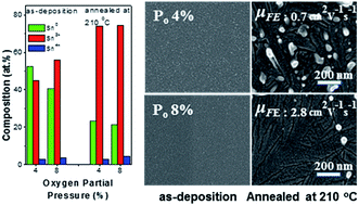
The composition-dependent structural and electrical properties of SnOx films prepared by means of reactive DC sputtering at various oxygen partial pressures (PO) and post-heat treatment temperatures (TA) were investigated, toward these films' potential use in p-channel oxide thin-film transistors (TFTs). A SnOx film fabricated under the lowest studied PO of 4% and heat-treated at 210 °C consisted of dendritic phases and irregular protrusions of metallic Sn. The resulting p-channel SnOx thin-film transistors suffered from marginal field effect mobility (μFE) and low on/off current ratio (ION/OFF), suggesting that the imperfect phases caused by oxygen-deficient stoichiometry hinder hole carrier conduction and act as bulk trap states. The heterogeneous structures observed in SnOx films annealed at 210 °C could be eliminated by increasing PO during fabrication. The resulting TFTs based on p-type SnOx films prepared at the high PO of 8% showed high mobilities up to 2.8 cm2 V−1 s−1 and reasonable ION/OFF of approximately 103, demonstrating the critical role of these films' homogeneous ordered aggregates without any imperfect phases such as a dendritic phase or irregular protrusions of metallic Sn. Among TFTs based on the films fabricated under 8% PO, the μFE and ION/OFF performance metrics degraded with increasing TA from 210 to 300 °C, which was mainly related to the 2SnO → SnO2 + Sn disproportionation reaction.
n-Type InGaZnO-based TFTs have been commercialized as backplane components of flat panel displays, yielding electron mobilities over 10 cm2 V−1 s−1.4 However, p-type MOSs still need to be improved. This discrepancy between types arises mainly from the difference in their band structures: in n-type oxide semiconductors, electrons are the majority carrier and are transported through a conduction band (CB) composed of delocalized s orbitals of metal ions, whereas in corresponding p-type materials, the valence band maximum (VBM) for transport of the majority hole carriers is composed of localized p orbitals of oxygen ions. Due to these characteristics of MOSs, electrons injected into MOS thin films are easily transferred along the conducting path and show better mobility regardless of structure ordering, relative to holes. Nevertheless, researchers have persistently studied p-type MOSs because they are necessary to fabricate inverters and/or logic circuits for low power consumption, application to transparent devices, etc.3
Stannous oxide (SnO) as a p-type MOS has a relatively large optical band gap of 2.7 eV, and thus has high visible transmittance of above 80%.4,5 Recently, it has been reported that in a SnO film the delocalized 5 s orbitals of Sn2+ at the edge of the VB could be controlled to have energy levels similar to that of the O 2p orbitals, thereby yielding high hole mobility in the resulting TFTs.6 It is known that Sn has the dual valency of 2+ and 4+. n-Type SnO2 (Sn4+) has a rutile structure with a tetragonal unit cell; in this structure, the Sn and O atoms have coordination numbers of 6 and 3, respectively. In contrast, p-type SnO (Sn2+) has a layered litharge structure having a Sn1/2–O–Sn1/2 sequence in the [001] direction, and wherein each Sn and O atom form a tetragonal unit.7,8
Due to competition arising from the dual valency of Sn, Sn-based oxide films sputtered under an oxygen partial pressure (PO) contain three phases: metallic Sn, SnO, and SnO2. In accordance with this, it has been recently reported that the different oxidized states of Sn in the corresponding thin films yield discernible differences in electrical, optical and micro structural properties of SnOx films prepared by magnetron sputtering.4,9–12 In particular, in the previous researches on the p-type SnOx based devices, the morphological evolution and related electrical properties in the SnOx thin films have been overlooked even though the morphological property can influence substantially the resulting electrical properties in other transparent oxide semiconductor TFTs.13,14 Only a couple of studies have mentioned on the microstructural evolutions by the heat treatment conditions where the clear explanations for the differences in the electrical properties in the SnOx thin films and resulting TFTs were not explicitly discussed.15,16 Accordingly, to achieve high performance in the p-type SnOx based field-effect transistors, systematic studies are still required to reveal out the oxidation state and/or microstructure dependency of their electrical properties.
In the present work we investigated the microstructural, morphological evolutions, phase transitions, and related electrical properties of SnOx thin films and their TFTs sputtered under conditions of various PO, before and after heat treatment at various temperatures (TA). The SnOx film prepared at the lowest PO of 4% and subsequently heat-treated at 210 °C consisted of dendritic phases and irregular protrusions of metallic Sn, which were facilitated by the oxygen-deficient stoichiometry in the films. These imperfect phases in the SnOx thin films could be eliminated by increasing PO conditions up to 8% during fabrication. The resulting p-channel SnOx TFTs which were fabricated under PO of 4% and subsequently heat-treated at 210 °C showed poor field effect mobility (μFE) of 0.73 cm2 V−1 s−1 and low on and off current ratio (ION/OFF) less than 10. Whereas the resulting TFTs prepared at the higher PO of 8% showed much improved mobilities up to 2.8 cm2 V−1 s−1 and ION/OFF of above 103, which underscores the critical role of the homogeneous ordered aggregates without dendritic phases and irregular protrusions of metallic Sn hindering hole carrier conduction and acting as bulk trap states in this material. By increasing TA from 210 to 300 °C, the μFE and ION/OFF of p-channel SnOx TFTs fabricated at PO under 8% were much degraded, which was attributed by the disproportionation reaction of SnOx thin films (2SnO → SnO2 + Sn).
Resistivity and carrier concentration of the SnOx thin films were evaluated using a four-point probe (CMT-SR1000N, Advanced Instrument Technology), and van der Pauw measurements of Hall mobility were conducted using a Hall effect measurement system (HL 5500 PC, Bio-Rad).17 Electrical characteristics of the SnOx TFTs were measured in a room-temperature dark chamber, using a semiconductor parameter analyzer (HP4155A, Hewlett-Packard).
The binding energy states of the Sn 3d5/2 core level yielded XPS peaks around 484.4, 485.9, and 486.6 eV, originating from oxidized states of Sn with three different oxidation numbers (i.e., Sn0, Sn2+, and Sn4+, respectively).18,19 XPS analysis of the Sn 3d5/2 core level in the SnOx sample prepared at the lowest PO of 4% indicated large portions of Sn0 and Sn2+: 52.2 and 45.0 at%, respectively. With increasing PO, the as-deposited films contained lesser portions of metallic Sn (Sn0), and no Sn0 was observed for the 12% PO sample: in this case, the Sn4+ state was also observed (see red curves around 486.6 eV in Fig. 1). After the films were heat-treated at 210 °C for 1 h, most of the Sn0 in the films was found to have oxidized to form SnO. Additionally, XPS spectra of the O 1s core levels in these SnOx films showed discernible oxygen states, depending on PO and heat treatment conditions. The binding energies of O–Sn2+ and O–Sn4+ were assigned as 529.8 and 530.4 eV, respectively.4,18–22
Fig. 2 is based on the XPS results and represents variations in the oxygen content and Sn oxidization states (Sn0, Sn2+, Sn4+) among SnOx films fabricated under various PO conditions, before and after heat treatment at 210 °C for 1 h. The detailed compositional variations were summarized at Table S1 in the ESI.† The oxygen content in as-deposited SnOx thin films increased monotonically from 24.3 to 43.5 at% with increasing PO from 4 to 12%. As PO was increased, the resulting portions of Sn0 decreased from 52.2 to 3.3% and the portions of Sn2+ and Sn4+ respectively increased from 45.0 to 84.7 at% and from 2.8 to 12.1 at%. During heat treatment, the metallic Sn atoms in the as-deposited films seemed to be mostly oxidized to Sn2+ instead of to Sn4+ (Fig. 2b): the portions of Sn4+ in the SnOx films were almost the same before and after heat treatment.
After heat treatment at 210 °C for 1 h, except for the 10% PO sample, all SnOx films showed intense X-ray reflections in 2D GIXD patterns that indicated ordered phases of metallic or oxidized Sn (Fig. 3). For the 4, 6, and 8% PO samples, intense X-ray reflections were observed that corresponded to polycrystalline SnO (JCPDS no. 01-085-0712) as well as β-phase Sn residue (see arrow-marked peaks in Fig. 3). For heat-treated 4, 6 and 8% PO samples, typical X-ray reflections were observed at Q of 1.297, 2.101, 2.334, and 2.594 Å−1, originating from the (001), (101), (110), and (002) planes in SnO crystallites with tetragonal unit cells: a = b = 3.796 Å, c = 4.816 Å.8 The X-ray reflections were anisotropically distributed along the X-ray Debye rings (Fig. 3), suggesting that the SnO aggregates were preferentially oriented with respect to the substrates. Interestingly, the heat-treated 8% PO SnOx film showed quite discernible orientations of (101), (110), and (200) planes in comparison to those in the 4 and 6% PO samples (this will be discussed later). However, the SnOx film samples with the highest O content (the 10 and 12% PO samples) retained amorphous-like structures even after heat treatment, suggesting that the presence of the secondary SnO2 phase strongly prevented crystallization and ordering of the primary SnO phase (approximately 76 at%, determined by XPS analysis). The XPS and GIXD results strongly supported the conclusion that the order of structures in the as-deposited and heat-treated SnOx films was degraded severely with increasing SnO2 composition.4
![]() | ||
| Fig. 3 (a) 2D GIXD patterns of SnOx films fabricated under PO of 4, 6, 8, and 10% and heat-treated at 210 °C for 1 h. (b–e) 1D in-plane and out-of-plane X-ray profiles extracted from the patterns shown in (a): (b) 4, (c) 6, and (d) 8% PO samples; (e) unit cell of the SnO lattice.3,7 Weak X-ray reflections marked with red arrows marked in (c) correspond to the β phase of Sn. | ||
Fig. 4 shows in-plane TEM micrographs of 15 nm-thick SnOx films fabricated under the PO of 4 and 8% and then heat-treated at 210 °C for 1 h. The 4% PO sample consisted mostly of polycrystalline SnO in which the (001) and (101) crystal planes were oriented normal to the dielectric surface (Fig. 4a inset). Additionally, less ordered grain boundaries were observed having 5–10 nm gaps (see broken line – marked region in Fig. 4a). In contrast, the SnO crystallites in the heat-treated 8% PO sample did not show any visible grain boundary: the (110) and (101) crystal planes were preferentially oriented normal to the dielectric surface (Fig. 4b). In this case, the angle between (110) and (101) planes was found to be about 64°, close to calculated value of 64.04° for the previously reported typical tetragonal structure of SnO.8 It was also found that the [001] direction (c-axis) in these crystallites was tilted from the surface normal, as evidenced by the 2D GIXD pattern (Fig. 3a). During reactive DC magnetron sputtering with a Sn target, fine control of PO is important to achieve preferential development of p-type SnO crystallites on dielectric surfaces; this leads to a discernible difference in the electrical properties of the resulting TFTs, as will be discussed below.26
Additional SEM and AFM analyses were carried out to investigate the morphologies of the SnOx thin films. All the as-deposited films showed very smooth and featureless morphologies, regardless of the PO during their fabrication (Fig. S2†). However, the heat-treated films all showed discernible structures that depended on the processing parameters of PO and TA. An SEM micrograph of the heat-treated 4% PO film showed a percolated layer including dendritic phases of widths ranging from 20 to 100 nm and vertically grown irregular protrusions with diameters on the order of several tens of nanometers. The dendritic grains and aggregates caused considerable inhomogeneity in this SnOx film, specifically, yielding severe lateral disconnection (Fig. 5a and S5 in ESI†). The irregular protrusions were determined by means of energy dispersive X-ray spectroscopy (EDS) analysis to be metallic Sn aggregates (Fig. S3†). The crystallites and aggregates in the 210 °C-heat-treated SnOx films became denser and less numerous with increasing PO (Fig. 5b and c). In contrast, the 10% PO samples showed featureless and smooth morphologies both before and after heat treatment (Fig. 5d).
![]() | ||
| Fig. 5 SEM micrographs of SnOx thin films fabricated under various PO and subsequently heat-treated at 210 °C for 1 h: (a) 4, (b) 6, (c) 8, and (d) 10% PO samples. | ||
Additionally, AFM topography analyses of the corresponding SnOx films showed similar morphologies as those indicated by the SEM results: increased oxygen content in the heat-treated SnOx films reduced the phase inhomogeneity and film surface roughness (Rq) (Fig. 6). Rq of the heat-treated films decreased drastically from 20.5 nm (at PO = 4%) to 0.4 nm (at PO = 10%) with increasing PO during their fabrication. Particularly, the Rq of 10% PO SnOx film was not changed after heat treatment at TA of 210 °C. The SEM and AFM results strongly supported the conclusion that the SnOx phase formation was very sensitive to oxygen stoichiometry and an equivalent oxygen stoichiometry was required to form the homogeneous p-type SnO phase from the as-deposited films.
![]() | ||
| Fig. 6 AFM phase images of SnOx films fabricated under various PO and subsequently heat-treated at 210 °C: (a) 4, (b) 6, (c) 8, and (d) 10% samples. | ||
Several studies have shown that the evolution of dendritic structures is enhanced when crystal growth rate exceeds the mass transport rate of ions and molecules that are necessary for crystal growth.27,28 Especially, Boggs et al.29 suggested reasonable mechanisms for the dendritic crystal growth of polycrystalline SnO phases during crystallization of SnOx thin films under oxygen-deficient conditions. Namely, they suggested that the areas adjacent to the crystallized SnO lattices become depleted in oxygen as the oxygen is captured and integrated into SnO lattices; consequently, further growth of SnO crystals must be directed toward areas that are richer in oxygen.
As shown in Fig. 2a, the SnOx thin films in this work were all deposited under oxygen-deficient conditions and then heat-treated in an oxygen-deficient atmosphere. Accordingly, the observation in the present work of the evolution of dendritic structures on surfaces of heat-treated SnOx thin films can be attributed to dendritic crystal growth of polycrystalline SnO phases in oxygen-deficient environments. Consequently, metallic Sn compositions in the oxygen-deficient areas adjacent to the dendritic structures would steadily increase until they exceeded their solubility limit, leading to phase separation and the formation of metallic Sn irregular protrusions. This explanation is supported well by the gradual disappearance of dendritic structures and irregular protrusions of metallic Sn observed with increasing PO from 4 to 8%. The reason why the heat-treated 10% PO sample showed a uniform surface is that the film had not yet crystallized.
Heat-treated semiconducting SnOx films (TA = 210 °C) were subjected to Hall effect measurements, in which they exhibited relatively high thermal stability. Fig. 7b shows net carrier concentration and μHall values for the SnOx thin films versus the PO used during their fabrication. The dominant carrier conduction for the 4, 6, and 8% PO films was determined to be p-type. The net hole concentration (Nh) for the SnOx films monotonically decreased from 4.35 × 10¹⁸ to 1.81 × 1018 cm−3 with increasing PO. This can be attributed to a reduction in free hole carriers in the overall SnOx film as the n-type SnO2 phase present in the film increases with increasing PO (see Table S1 in the ESI†).4 Conversely, the films' μHall values increased from 1.1 to 5.5 cm2 V−1 s−1 with increasing PO. The differences in crystallographic preferential orientation and topological evolution of the SnOx film depending on PO during deposition can be considered the most plausible origin for the observed variation in μHall. The electronic structure reported by Togo et al.6 suggests that the stannous oxide (SnO) has an anisotropic band structure in its Brillouin zone. The curvature of the E–k diagram in the [001] direction (Γ–Z) is larger than those in the [100] direction (Γ–X) and [110] direction (Γ–M) near the VBM. This means that the effective hole mass
in the [001] direction is the smallest among the various directions. From this, one would predict that 4% PO films showed higher mobility than 8% PO films because the volume faction of [001] oriented parallel to the in-plane direction was substantially higher in the former, however, as shown in Fig. 7b, this is not the case. In general, the carrier mobility is proportional to the product of the mean scattering time and inversely proportional to the effective mass. Therefore, it can be inferred that the carrier scattering mechanism plays a critical role in determining the carrier mobility. Indeed, the 4% PO film suffered from microstructural inhomogeneities such as metallic Sn aggregates and dendritic structure. These imperfections are likely to act as strong scattering centers, and thus to be responsible for this material's inferior mobility.
The electrical functionality of these p-type semiconducting SnOx films was further evaluated in thin-film transistors (TFTs) made from the films. Fig. 8a shows representative transfer characteristics for bottom gate SnOx TFTs with 15 nm-thick channels made using the 4, 6, and 8% PO films. The field-effect mobility (μFE) and subthreshold gate swing (SS) were respectively calculated using eqn (1) and (2), given below. The maximum bulk trap density (NSS,max) and interfacial trap density (Dit,max) were evaluated using eqn (3), for which the value of NSS,max (Dit,max) was estimated by setting the Dit,max (NSS,max) term to zero.
![]() | (1) |
![]() | (2) |
SS = qkBT(NSS,maxtch + Dit,max)/[Ci log(e)]
| (3) |
![]() | ||
| Fig. 8 (a) Transfer and (b) output characteristics of bottom gate structure TFTs based on thin SnOx films (15 nm-thick) fabricated under various PO (4, 6, and 8%) and heat-treated at 210 °C. | ||
All the SnOx TFTs exhibited p-type conduction irrespective of the PO values. The SnOx TFT prepared at PO = 4% showed the marginal μFE of 0.73 cm2 V−1 s−1, and yielded the low ION/OFF ratio of 6.8, representing poor current modulation capability. The device performance of the SnOx TFTs was improved for films deposited under greater PO. The high μFE of 2.8 cm2 V−1 s−1 and reasonable ION/OFF ratio of 1.0 × 10³ were achieved by the SnOx TFT based on the 8% PO film, as shown in Fig. 8a and Table 1. The superior performance of the SnOx TFT based on the 8% PO film underscores the importance of its homogenous ordered aggregate state and its absence of Sn metal aggregate and abrupt dendritic structure.
| PO (%) | Nh (cm−3) | μHall (cm2 V−1 s−1) | ION/OFF | μFE (cm2 V−1 s−1) | SS (V dec−1) | NSS,max (eV−1 cm−3) | Dit,max (eV−1 cm−2) |
|---|---|---|---|---|---|---|---|
| a Note: the electrical properties of SnOx thin films fabricated under PO of 10 and 12%, and TFTs fabricated based on these films, were not measurable due to their excessive resistivity. | |||||||
| 4 | 4.35 × 10¹⁸ | 1.14 | 6.8 × 100 | 0.73 | 62.9 | 1.52 × 10²⁰ | 2.28 × 10¹⁴ |
| 6 | 2.64 × 10¹⁸ | 2.84 | 2.9 × 101 | 1.21 | 27.6 | 6.64 × 10¹⁹ | 9.96 × 10¹³ |
| 8 | 1.81 × 10¹⁸ | 5.49 | 1.0 × 10³ | 2.80 | 8.47 | 2.03 × 10¹⁹ | 3.05 × 10¹³ |
It is interesting to discuss why the SnOx TFT based on the 4% PO film yielded the poor ION/OFF ratio of 6.8. The observation of high off-state IDS indicated the difficulty in fully depleting the bulk semiconducting SnOx film. In other words, the quasi Fermi level (EF) in the SnOx film near the gate dielectric/semiconductor interface was strongly pinned due to the very large NSS because EF cannot move upward without trap filling.31 Indeed, the extracted NSS,max value for the TFTs based on 4% PO film was the largest measured (1.5 × 10²⁰ eV−1 cm−3). Contrastingly, NSS,max for the TFTs based on 8% PO film was 2.0 × 10¹⁹ eV−1 cm−3. The superior transporting property of these TFTs was clearly reflected in the higher IDS level of their output characteristics (see Fig. 7b).
A qualitatively similar trend for the p-channel SnOx TFTs based on the 4, 6, and 8% PO films heat-treated at TA of 210 °C was also observed for higher TA (240, 270, and 300 °C; Fig. S4†). Interestingly, the μFE value and ION/OFF ratio observed for a SnOx TFT at a given PO condition were degraded by increasing TA from 210 to 300 °C. For example, the TFTs based on the 8% PO film and heat-treated at 300 °C yielded μFE of 1.0 cm2 V−1 s−1 and the ION/OFF ratio of 1.6 × 10². This behavior can also be attributed to a structural transition involving the chemical states of Sn ions and microstructural inhomogeneity, namely, phase separation from 2SnO to SnO2 plus metallic Sn; this transition is thermodynamically driven above 250 °C.32,33
Finally it would be meaningful to compare the performance of SnO TFTs in this study with other works. The μFE of 2.8 cm2 V−1 s−1 and ION/OFF ratio of 1.0 × 10³ for the SnOx TFT based on the 8% PO film are comparable to those (μFE: 1.7–6.8 cm2 V−1 s−1, ION/OFF ratios of 103 to 104) reported in the literature for other p-channel oxide TFTs.4,11,15,34–38 It should be noted that higher mobility (≥3.3 cm2 V−1 s−1) can be achieved further by adopting the high permittivity dielectric films such as HfO2,11 AlTiOx,36 and/or reducing the gate insulator thickness.34,35
| DC | Direct current |
| MOSs | Metal oxide semiconductors |
| LCs | Liquid crystals |
| OLEDs | Organic light emitting diodes |
| TFTs | Thin-film transistors |
| CB | Conduction band |
| VBM | Valence band maximum |
| S/D | Source/drain |
| SE | Spectroscopic ellipsometry |
| XPS | X-ray photoelectron spectroscopy |
| GIXD | Grazing-incidence X-ray diffraction |
| TEM | Transmission electron microscopy |
| EDS | Energy dispersive X-ray spectroscopy |
| SEM | Scanning electron microscopy |
| AFM | Atomic force microscopy |
012) Sapphire, J. Appl. Phys., 2001, 89(11), 6056–6061 CrossRef CAS Footnote |
| † Electronic supplementary information (ESI) available: Summarizations of the chemical compositions of Sn (Sn0, Sn2+, and Sn4+) and O content in SnOx films fabricated under various PO conditions, additional details on the 2D GIXD patterns of as-deposited SnOx films, SEM images of as-deposited SnOx thin films, energy dispersive X-ray spectroscopy (EDS) analysis of atomic composition in the irregular protrusions of SnOx thin films, TFT performance metrics extracted from transfer characteristics of bottom gate TFTs prepared using SnOx thin films, SEM micrographs of 45 nm-thick SnOx films annealed at 210 °C for 1 h. See DOI: 10.1039/c6ra08726d |
| This journal is © The Royal Society of Chemistry 2016 |