Hydrobromic acid assisted crystallization of MAPbI3−xClx for enhanced power conversion efficiency in perovskite solar cells

Jin Huanga, Minqiang Wang*a, Lei Dingb, Zhi Yanga and Ke Zhanga
aElectronic Materials Research Laboratory (EMRL), Key Laboratory of the Ministry of Education, International Center for Dielectric Research, Xi'an Jiaotong University, Xi'an 710049, China. E-mail: huangjin86@stu.xjtu.edu.cn; mqwang@mail.xjtu.edu.cn
bCollege of Science, Shaanxi University of Science and Technology, Xi'an 710021, China

Received 22nd March 2016 , Accepted 29th April 2016

First published on 24th May 2016


Abstract

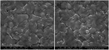
Enhanced performance of perovskite solar cells based on the application of high quality MAPbI3−xClx films developed via a hydrobromic acid assisted fast crystallization process is reported. A current density (Jsc) of 21.71 mA cm−2, an open circuit voltage (Voc) of 0.94 V, a fill factor (FF) of 0.77 and a high power conversion efficiency (PCE) of 15.76% were obtained. Noticeably, the hydrobromic acid assisted device exhibited less hysteresis and followed a crystallization route which is several times faster than that of the traditional one-step spin-coating method. The enhancement in device performance is attributed to the increased parallel resistance, lower leakage current, reduced series resistance and stronger crystallization of the MAPbI3−xClx perovskite layer.


1. Introduction

Organic–inorganic perovskite solar cells have emerged as the most promising in the field of thin film photovoltaics in recent years. Their power conversion efficiency (PCE) has currently gone beyond 20%.1–18 The fabrication of high quality perovskite films is prerequisite to achieving a highly efficient perovskite solar cell.19–22 This stems from the fact that the performance of perovskite solar cells depends on the degree of coverage and crystal quality of the perovskite layer.18–22 Currently, there exist two main methods for growing hybrid perovskite films. One follows a one-step spin-coating pathway, utilizing perovskite precursor solutions (modified or not) while the other follows a two-step spin-coating pathway which involves an initial deposition of PbI2 and its subsequent conversion to perovskite film.23–26

As is known, there exist many reported methods for the enhancement of film quality using additives.37–40 For example, the addition of H2O,39 HCl,39 HI40 and so on37,38 as intermediate phases allows the formation of well defined precrystallized domains before annealing.37 Achieving a compact and uniform film is crucial to the planar structure of the fabricated device. This research therefore focuses on the realization of highly crystalline and uniform perovskite film with complete coverage for the fabrication of planar perovskite solar cell (PSC). It is required to design a new method of growing a high quality perovskite film. This is to avoid the interface current and leakage current usually existing in films grown via the one-step deposited process.27–30

In this paper, we adopted the use of halogen ion which is a strong donor that can interact strongly with Pb2+ and as a result form a homogeneous solution which is beneficial for the growth of high quality films.38,39 Particularly, we demonstrated a method to achieve fast formation and crystallization of MAPbI3−xClx films by the introduction of 47 wt% hydrobromic acid (HBr) into the perovskite precursor solutions. When the HBr modified precursor solutions were spin-coated, a precrystallized intermediate state was formed before the annealing step.37 Consequently, a perovskite solar cell with lower leakage current, better surface coverage and stronger crystallization of the MAPbI3−xClx perovskite film was fabricated. Notably, the HBr modified perovskite solar cell with a planar structure exhibited less hysteresis.

2. Experimental section

2.1. Solar cell fabrication

Perovskite precursor (30 wt%) synthesis: 3[thin space (1/6-em)]:[thin space (1/6-em)]1 (molar ratio) of MAI and PbCl2 (Alfa Aesar) was mixed in DMF (N,N-dimethylformamide) at 60 °C for 10 hour under stirring. Hydrobromic acid (7 vol%) from 47% hydrobromic acid was then added into the perovskite precursor solution. A reference device was also fabricated using the same method.

ITO-coated glass substrates were cleaned with the sequential use of: boiling deionized water, boiling EtOH and oxygen plasma.

Compact TiO2 film was initially deposited from a precursor solution of titanium isopropoxide (0.3 M, Alfa Aesar) and HBr (0.01 M) in ethanol. This precursor solution was spin-coated at 3500 rpm, for 30 s on the cleaned ITO-coated glass substrates. The resulting film was then annealed at 400 °C in a muffle furnace to ensure good crystallization.31 The perovskite precursor solutions were spin-coated at 4000 rpm for 30 s. The films obtained were annealed on a hot plate at 100 °C for 5 min to promote the crystallization of MAPbI3−xClx. When the substrates were cooled to room temperature, Spiro-OMETAD (70 mg ml−1 in chlorobenzene with additives (4-tert-butylpyridine and bis(trifluoromethanesulfonyl)imide))23 was deposited on the perovskite films by spin-coating at 2000 rpm for 30 s. Finally, silver cathode was deposited on the Spiro-OMETAD layer by thermal evaporation at a rate of 0.1–0.3 nm s−1. The film thickness obtained was about 100 nm. A device area of 7.25 mm2 was defined with a shadow mask. Reference PSCs were also fabricated with the same device structure. These devices were fabricated following the traditional method.32

The fabricated planar structure of the perovskite solar cells is given as ITO/TiO2/MAPbI3−xClx/Spiro-OM ETAD/Ag.

2.2. Measurements and characterization

Current density–voltage (JV) measurements were taken in air by using a Keithley 2400 source meter. A standard Si solar cell was utilized to calibrate the light intensity of AM1.5G solar simulator (Sciencetech Inc., SS-150) which is 100 mW cm−2. Electrochemical impedance spectroscopy study was conducted on the devices by using an electrochemical workstation (CHI660D, Chenhua, Shanghai). The solar cell quantum efficiency measurements were taken on a certified IPCE instrument known as 7-SCSpec II system, NewPort. The measurements were taken within a range of 300 nm to 800 nm at an interval of 5 nm. Surface morphologies of MAPbI3−xClx films were measured with FEI Quata 250FEG scanning electron microscope. Jasco V-570 UV-Visible spectrophotometer was used for the optical absorption measurements of MAPbI3−xClx precursor solutions. X-ray diffraction (XRD) measurements were conducted with a D/max-2400 X-ray diffraction spectrometer (Rigaku, Japan).

3. Results and discussion

As know, the surface morphology and quality of the MAPbI3−xClx film determine the performance of planar MAPbI3−xClx based perovskite solar cells.19–22 HBr modified precursor solution was applied in improving the quality and morphology of the perovskite film. Two fabrication methods which involve the use of precursor solutions with and without HBr were illustrated in the preceding section on solar cell fabrication. Fig. 1(a) and (b) show the SEM images of MAPbI3−xClx films prepared on ITO/TiO2 surface without and with HBr modification respectively. It can be seen in Fig. 1(b) that the HBr modified MAPbI3−xClx film also can be fabricated a compact morphology with full coverage. These compactness and full coverage effectively prevent contact between electron transfer layer (ETL) and hole transfer layer (HTL). The film without HBr modification showed incomplete surface coverage with many voids showing up on the film. These SEM images signify that the devices fabricated with HBr modification exhibit better performance and less leakage current (Fig. 6(b)).
image file: c6ra07536c-f1.tif
Fig. 1 SEM images of MAPbI3−xClx perovskite films grown on ITO/TiO2 surface (a) without and (b) with HBr modification.

Fig. 2(a) shows the corresponding XRD patterns of MAPbI3−xClx films with and without HBr modification. It is observed that the MAPbI3−xClx with HBr modification possesses more intense scattering peak in 14.17° and 28.51°, and that no peak of PbI2 is observed at 12.23°.33 This confirms better crystallization for the MAPbIxCl3−x film with HBr modification. The UV-vis absorption curve of MAPbI3−xClx is consistent with previous reports. From Fig. 2(a), it is seen that HBr modification is beneficial to the crystal quality of MAPbI3−xClx. The improved homogeneity of the precursor solution corresponding to the HBr modified MAPbI3−xClx is responsible for the observed reduction in the UV-vis absorption in Fig. 2(b) and the expected increase in UV-vis transmission. As know, high quality films are derived from homogeneous solutions. This is in accord with SEM image of the Fig. 1. The UV-vis absorption curve of MAPbI3−xClx in Fig. 2(b) exhibits an edge at 800 nm which agrees well with the external quantum efficiency (EQE) spectra (Fig. 3(b)).


image file: c6ra07536c-f2.tif
Fig. 2 (a) X-ray diffraction patterns and (b) UV-vis absorption curve of MAPbI3−xClx with and without HBr modification, the zoom-in plot of inset is from 600 nm to 800 nm.

image file: c6ra07536c-f3.tif
Fig. 3 (a) JV curve and (b) external quantum efficiency (EQE) spectra of MAPbI3−xClx perovskite solar cells with and without HBr modification.

From Fig. 3(a), The HBr modified device exhibits higher Jsc, Voc and FF. The JV curves also illustrate that HBr modified perovskite precursor solution can yield better MAPbI3−xClx film. Fig. 3(b) also exhibits these characteristics, as the HBr modified perovskite solar cell shows better external quantum efficiency, which is in agreement with the better JV (current density–voltage) properties presented in Table 1 and Fig. 3(a). Within the wavelength range of 500 nm to 700 nm, the HBr modified device presents obvious enhancement (Fig. 3(b)), and the reduced absorption of MAPbI3−xClx shown in Fig. 2(b) reveals that HBr modification enhances the formation of MAPbI3−xClx. Therefore, according to Fig. 3(b) and 2(b), the blue shift of UV-vis spectra is ascribed to added HBr, however, the red shift of EQE is ascribed to high quality perovskite films with HBr modified, because the finally perovskite have no Br ions (Fig. S1). To clearly show the improved performance observed in the HBr modified device, photovoltaic parameters of the perovskite solar cells with and without HBr modification are presented in Table 1. The modification process enhances the PCE from 12.13% to 15.76%, Voc from 0.87 V to 0.94 V, Jsc from 19.12 mA cm−2 to 21.71 mA cm−2 and fill factor from 0.72 to 0.77. These results indicate that good film quality can promote charge extraction and collection processes. The observed higher shunt resistance (Rsh) and lower series resistance (Rs) are beneficial for charge transport and extraction.34,35 From Table 1, devices fabricated with other halogen ion modification show similar improvement. However, HBr gave the best result. This Br ion enhancement of perovskite solar cell performance41 stems from the formation of a better intermediate phase in perovskite film growth before annealing.37 The addition of H2O also enhances the performance of MAPbI3−xClx based perovskite solar cell, however, the halogen ion interaction with Pb2+ proved to be the most important factor in the growth of MAPbI3−xClx films (Table 1).

Table 1 Photovoltaic parameters of the perovskite solar cells with and without HBr, HI, HCl and H2O additives
Devices Voc (V) Jsc (mA cm−2) Fill factor Rs/Rsh PCE (%) average PCE (%) best
MAPbI3−xClx 0.87 19.12 0.72 9.07/2412.63 10.22 12.13
MAPbI3−xClx[thin space (1/6-em)]:[thin space (1/6-em)]HBr 0.94 21.71 0.77 3.71/3070.89 13.13 15.76
MAPbI3−xClx[thin space (1/6-em)]:[thin space (1/6-em)]HI 0.91 21.13 0.71 4.97/2682.36 12.64 14.41
MAPbI3−xClx[thin space (1/6-em)]:[thin space (1/6-em)]HCl 0.90 21.11 0.72 5.43/2574.39 12.76 13.67
MAPbI3−xClx[thin space (1/6-em)]:[thin space (1/6-em)]H2O 0.90 19.84 0.71 6.15/2596.14 11.34 12.67


Fig. 4(a) presents the JV curve of the champion MAPbI3−xClx-based device. The photovoltaic parameters of the champion device tested under AM1.5G solar illumination are a PCE of 15.76%, a Voc of 0.94 V, an FF of 0.77 and a Jsc of 21.71 mA cm−2. These parameters confirm that the film coverage and compactness, UV-vis absorption and crystallinity are in a better state in the HBr modified device. Fig. 4(c) shows the PCE of modified MAPbI3−xClx perovskite solar cell with histogram of 30 devices. There are no significant changes in PCE. The HBr-modified solar cell therefore shows good reproducibility.


image file: c6ra07536c-f4.tif
Fig. 4 (a) JV curve of the champion MAPbI3−xClx-based device. (b) PCE histogram of 30 devices for the modified MAPbI3−xClx perovskite solar cell.

Fig. 5 shows the JV curves of HBr-modified device scanned from different directions. It can be seen that there is no significant JV hysteresis. This shows that the fabricated PSC has a good balance of charge extraction and transport. The photovoltaic parameters for the representative HBr-modified device scanned in forward and reverse directions are shown in Table 2. These parameters show that HBr modification of MAPbI3−xClx PSC can decrease the JV hysteresis in the forward and reverse scan and can also enhance charge extraction and transport in the device.


image file: c6ra07536c-f5.tif
Fig. 5 Representative HBr-modified device scanned from different directions.
Table 2 Photovoltaic parameters of the representative HBr-modified device scanned from different directions
Devices Voc (V) Jsc (mA cm−2) Fill factor PCE (%)
Forward 0.95 21.42 0.73 15.05
Reverse 0.94 21.72 0.77 15.76


Fig. 6(a) shows the Nyquist plots of MAPbI3−xClx perovskite solar cells with and without HBr modification which was carried out at the Voc of the perovskite solar cells. A significant difference is observed in the electrical properties of the PSCs. The impedance spectroscopy (IS) study shows the series resistance (RS) of connected functional layers in the perovskite solar cells with and without HBr modification. The internal series resistance includes the interfaces of MAPbI3−xClx layer and charge selective layers, the MAPbI3−xClx bulk, the exciton transfer resistance (RCT) at the interfaces of electrode and exciton transport layers and the electrodes' sheet resistances (RSheet).36 The diameters of the Nyquist plots indicate the internal series resistance. The HBr modified device exhibits less RS, owning to its shorter Nyquist plot diameter. This also gives the reason why the JV curve of the HBr modified device indicates better charge extraction and transport as the film with HBr modification made better interface contact with Spiro-OMETAD and TiO2. From the Tafel curve of symmetric cells (Fig. 6(b)), it is seen that the perovskite solar cells with HBr modification exhibits less dark current in the log(J)–V plot at the reversed bias region. The reduced dark current is determined by the quality of the film (compactness, coverage and crystallinity),28,29 as presented in the SEM images (Fig. 1(b)).


image file: c6ra07536c-f6.tif
Fig. 6 (a) Nyquist plots of MAPbI3−xClx perovskite solar cells with and without HBr modification tested under applied voltage conditions approaching the Voc of perovskite solar cells with the device structure of ITO/TiO2/MAPbI3−xClx/Spiro-OMETAD/Ag. (b) Tafel curve for symmetric perovskite solar cells with and without HBr modification tested in dark condition.

4. Conclusion

In summary, planar HBr modified MAPbI3−xClx-based perovskite solar cells were successfully fabricated with a high PCE of 15.76% and a high quality perovskite film prepared from a modified precursor solution process. We demonstrated that the precursor solution plays a critical role in the formation and crystallization of perovskite films. As a result, the halogen ion modified MAPbI3−xClx-based PSC shows less series resistance and better performance than that of the device fabricated following the conventional deposition and crystallization procedure. The halogen ion modified devices yielded better results than the H2O modified devices as the halogen ions played an important role in the modification process. However, Br ion yielded the best result. The enhanced performance obtained for the fabricated perovskite solar cell is due to the increased parallel resistance, reduced series resistance and lower leakage current exhibited by the device as a result of the better film quality and stronger crystallization for the MAPbI3−xClx film. This work presents a feasible method to fabricate and improve the performance of MAPbI3−xClx based planer PSC.

Acknowledgements

The authors gratefully acknowledge financial support from Natural Science Foundation of China (NSFC Grant No. 51572216). This work has been financially supported by NSFC Major Research Program on Nano manufacturing (Grant No. 91323303), the Industrial Science and Technology research project in Shaanxi province (2015GY005), 111 Program (No. B14040) and the open projects from Institute of Photonics and Photo-Technology, Provincial Key Laboratory of Photoelectronic Technology, Northwest University, China.

References

  1. D. D. Lin, H. Wu, W. Zhang, H. P. Li and W. Pan, Appl. Phys. Lett., 2009, 94, 172103 CrossRef.
  2. Z. X. Wang, X. Y. Zhan, Y. J. Wang, S. Muhammad, Y. Huang and J. He, Nanoscale, 2012, 4, 2678–2684 RSC.
  3. Q. Chen, H. Zhou, Z. Hong, S. Luo, H.-S. Duan, H.-H. Wang, Y. Liu, G. Li and Y. Yang, J. Am. Chem. Soc., 2013, 136, 622 CrossRef PubMed.
  4. S. K. Tzeng, M. H. Hon and I. C. Leu, J. Electrochem. Soc., 2012, 159, H440–H443 CrossRef CAS.
  5. K. Liu, M. Sakurai, M. Y. Liao and M. Aono, J. Phys. Chem. C, 2010, 114, 19835–19839 CAS.
  6. M. Xiao, F. Huang, W. Huang, Yi-B. Cheng and L. Spiccia, Angew. Chem., 2014, 126, 1–7 CrossRef.
  7. G. Li, V. Shrotriya, J. Huang, Y. Yao, T. Moriarty, K. Emery and Y. Yang, Nat. Mater., 2005, 4, 864 CrossRef CAS.
  8. S. Sista, Mi-H. Park, Z. Hong, Y. Wu, J. Hou, W. L. Kwan, G. Li and Y. Yang, Adv. Mater., 2010, 22, 380–383 CrossRef CAS PubMed.
  9. M. Xiao, F. Huang, W. Huang, Y. Dkhissi, Y. Zhu, J. Etheridge, A. Gray-Weale, U. Bach, Y. B. Cheng and L. Spiccia, Angew. Chem., Int. Ed., 2014, 126, 10056 CrossRef.
  10. G. Li, Y. Yao, H. Yang, V. Shrotriya, G. Yang and Y. Yang, Adv. Funct. Mater., 2007, 17, 1636 CrossRef CAS.
  11. X. Liu, H. Wang, T. Yang, W. Zhang and X. Gong, ACS Appl. Mater. Interfaces, 2012, 4, 3701 CAS.
  12. N. J. Jeon, J. H. Noh, Y. C. Kim, W. S. Yang, S. Ryu and S. II Seok, Nat. Mater., 2014, 13(9), 4014 Search PubMed.
  13. X. W. Fu, Z. M. Liao, Y. B. Zhou, H. C. Wu, Y. Q. Bie, J. Xu and D. P. Yu, Appl. Phys. Lett., 2012, 100, 223114 CrossRef.
  14. A. Kim, Y. Won, K. Woo, C. H. Kim and M. Jooho, ACS Nano, 2013, 7, 1081–1091 CrossRef CAS PubMed.
  15. R. M. Mutiso, M. C. Sherrott, A. R. Rathmell, B. J. Wiley and K. I. Winey, ACS Nano, 2013, 7, 7654–7663 CrossRef CAS PubMed.
  16. A. Dualeh, T. Moehl, P. Gao, M. K. Nazeeruddin and M. Grätzel, Funct. Mater, 2014, 24, 3250–3258 CrossRef CAS.
  17. S. Liu, J. F. Ye, Y. Cao, Q. Shen, Z. F. Liu, L. M. Qi and X. F. Guo, Small, 2009, 5, 2371–2376 CrossRef CAS PubMed.
  18. M. J. Carnie, C. Charbonneau, M. L. Davies, J. Troughton, T. M. Watson, K. Wojciechowski, H. Snaith and D. A. Worsley, Chem. Commun., 2013, 49, 7893–7895 RSC.
  19. J. Huang, M. Wang, L. Ding, F. Igbari and X. Yao, Sol. Energy, 2016, 130, 273–280 CrossRef CAS.
  20. X. Li, M. Ibrahim Dar, C. Yi, J. Luo, M. Tschumi, S. M. Zakeeruddin, M. K. Nazeeruddin, H. Han and M. Grätzel, Nat. Chem., 2015, 7, 703–711 CrossRef CAS PubMed.
  21. J. H. Heo, D. H. Song and S. H. Im, Adv. Mater., 2014, 26, 8179–8183 CrossRef CAS PubMed.
  22. Y. Zhao and K. Zhu, J. Mater. Chem. A, 2015, 3, 9086–9091 CAS.
  23. J. Huang, M. Wang, L. Ding, J. Deng and X. Yao, Semicond. Sci. Technol., 2016, 31, 025009 CrossRef.
  24. G. Li, T. Zhang and Y. Zhao, J. Mater. Chem. A, 2015, 3, 19674–19678 CAS.
  25. B. Conings, A. Babayigit, T. Vangerven, J. D'Haen, J. Manca and H.-G. Boyen, J. Mater. Chem. A, 2015, 3, 19123–19128 CAS.
  26. W. Zhang, S. Pathak, N. Sakai, T. Stergiopoulos, P. K. Nayak, N. K. Noel, A. A. Haghighirad, V. M. Burlakov, D. W. Quilettes, A. Sadhanala, W. Li, L. Wang, D. S. Ginger, R. H. Friend and H. J. Snaith, Nat. Commun., 2015, 6, 10030 CrossRef CAS PubMed.
  27. Q. Xue, Z. Hu, C. Sun, Z. Chen, F. Huang, H.-L. Yip and Y. Cao, RSC Adv., 2015, 5, 775–783 RSC.
  28. M. Qian, M. Li, X.-B. Shi, H. Ma, Z.-K. Wang and L.-S. Liao, J. Mater. Chem. A, 2015, 3, 13533–13539 CAS.
  29. W. Chen, Y. Wu, Y. Yue, J. Liu, W. Zhang, X. Yang, H. Chen, E. Bi, I. Ashraful, M. Grätzel and L. Han, Science, 2015, 350, 6263, 944–948 Search PubMed.
  30. L. Dou, Y. (Micheal) Yang, J. You, Z. Hong, W.-H. Chang, G. Li and Y. Yang, Nat. Commun., 2014, 5(5404), 1–6 Search PubMed.
  31. Q. Jiang, X. Sheng, Y. Li, X. Feng and T. Xu, Chem. Commun., 2014, 50, 14720–14723 RSC.
  32. J. M. Ball, M. M. Lee, A. Hey and H. J. Snaith, Energy Environ. Sci., 2013, 6, 1739–1743 CAS.
  33. H. Zhou, Q. Chen, G. Li, S. Luo, T.-B. Song, H.-S. Duan, Z. Hong, J. You, Y. Liu and Y. Yang, Science, 2014, 345(6196), 542–546 CrossRef CAS PubMed.
  34. V. Gonzalez-Pedro, E. J. Juarez-Perez, W.-S. Arsyad, E. M. Barea, F. Fabregat-Santiago, I. Mora-Sero and J. Bisquert, Nano Lett., 2014, 14, 888–893 CrossRef CAS PubMed.
  35. C. Liu, Z. Qiu, W. Meng, J. Chen, J. Qi, C. Dong and M. Wang, Nano Energy, 2015, 12, 59–68 CrossRef CAS.
  36. J.-S. Kim, W.-S. Chung, K. Kim, D. Y. Kim, K.-J. Paeng, S. M. Jo and S.-Y. Jang, Adv. Funct. Mater., 2010, 20, 3538 CrossRef CAS.
  37. C.-C. Chen, Z. Hong, G. Li, Q. Chen, H. Zhou and Y. Yang, J. Photonics Energy, 2015, 5, 057405 CrossRef.
  38. F. K. Aldibaja, L. Badia, E. Mas-Marz, R. S. Sanchez, E. M. Barea and I. Mora-Sero, J. Mater. Chem. A, 2015, 3, 9194–9200 CAS.
  39. G. Li, T. Zhang and Y. Zhao, J. Mater. Chem. A, 2015, 3, 19674–19678 CAS.
  40. F. Wang, H. Yu, H. Xu and N. Zhao, Adv. Funct. Mater., 2015, 25, 1120–1126 CrossRef CAS.
  41. D. Bi, W. Tress, M. I. Dar, P. Gao, J. Luo, C. Renevier, K. Schenk, A. Abate, F. Giordano, J.-P. Correa Baena, J.-D. Decoppet, S. M. Zakeeruddin, M. K. Nazeeruddin and M. Grätzel, Anders Hagfeldt. Sci. Adv., 2016, 2, e1501170 Search PubMed.

Footnote

Electronic supplementary information (ESI) available. See DOI: 10.1039/c6ra07536c

This journal is © The Royal Society of Chemistry 2016
Click here to see how this site uses Cookies. View our privacy policy here.