Paper-based SERS active substrates on demand

Pushkaraj Joshi and Venugopal Santhanam*
Department of Chemical Engineering, Indian Institute of Science, Bangalore-560012, India. E-mail: venu@chemeng.iisc.ernet.in

Received 19th March 2016 , Accepted 2nd July 2016

First published on 13th July 2016


Abstract

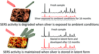
Surface Enhanced Raman Spectroscopy (SERS) is an important technique for molecular analysis under ambient conditions, and the use of paper-based silver nanostructures as a disposable SERS substrate is an attractive option for low-cost, point-of-use analysis. However, the activity of pre-fabricated silver nanostructures is affected by tarnishing and necessitates either storage under inert gas conditions or use of a protective layer on the surface. But neither of these approaches are satisfactory in terms of cost and performance in real-world settings. To address this, we report a print-expose-develop process, based on silver-halide photography, to fabricate SERS active silver nanowire networks on demand using a desktop inkjet printer. This process involves only the printing of silver and halide salt solutions and obviates the need for complex colloidal ink formulation steps reported in earlier studies on inkjet printed SERS substrates. Significantly, the printed and photo-exposed silver halide films retain silver in a stable latent-image form for more than 1 year under ambient conditions. Upon demand at the point-of-use, the latent silver can be easily developed into highly active SERS-active nanostructures, with average EF ∼104, by dipping in a standard photographic developer solution and rinsing.


Introduction

Surface Enhanced Raman Spectroscopy (SERS) is a label-free, point-of-use spectroscopic technique capable of exhibiting high selectivity,1 based on molecular fingerprinting, and sensitivity,2 even at single-molecule detection levels. SERS based sensors with applications in a wide variety of analytical3–6 or bioanalytical7 or material characterization8 settings have been developed. The surface enhancement comprises an electromagnetic effect and a charge-transfer effect. The nanostructured metal substrate is the key factor that controls the electromagnetic effect, which is considered to be a dominant factor and to be present in all situations.9 Therefore, significant research effort has gone into fabricating SERS substrates with characteristics like high sensitivity, signal uniformity, and reproducibility.10

In the early stages of SERS development, analytes were added into silver colloidal solutions so as to sandwich molecules within 'hot spots' formed by nanoparticle flocculation, yielding high Raman signal enhancements, albeit random and transitory in nature.11 However, for most common applications, prefabricated SERS substrates are the key for commercialization. Over the last two decades, there has been rapid advancement in terms of uniformity, stability and reproducibility of silicon-based SERS substrates decorated with nanoscale plasmonic features, either using top-down or bottom-up approaches.12 Flexible substrates, such as paper or plastic films, are gaining wide recognition as disposable, low-cost, SERS substrates.10 Moreover, paper enables pre-concentration of samples by using configurations such as dipsticks,13,14 filters,15 swabs,4,16,17 and lateral-flow,14,18 as well as easy integration with low-cost paper-based micro/optofluidic platforms.19 Paper is also sought-after for being easily disposable by burning, which is of importance in bioanalytics.15 Finally, paper is a substrate with hierarchical roughness that can lead to larger surface area serving as a platform for plasmonic interactions between multiple layers.20,21

Paper based SERS substrates have been fabricated either by depositing nanostructures using seeded growth,4 self-assembly,16 adsorption from colloidal solution,20,21 brushing,22 filtration,23 inkjet printing,14,24 physical vapour deposition,25,26 screen printing,27 or by in situ formation using chemical reduction.3,28 Amongst these, the use of additive drop-on-demand printing technology offers a cost-effective route for manufacturing of SERS substrates. But, the various steps involved in colloidal ink formulation, such as synthesis of colloid from precursor salts, their subsequent concentration by centrifugation, addition of various molecules for modification of viscosity and surface tension, as well as surfactants for enhancing storage life, are both tedious and costly. Utilization of standard office desktop inkjet printers for fabricating SERS substrates can only be easily adapted in most parts of the world, if complex colloidal ink formulation steps are eliminated.

Furthermore, in an effort to enhance shelf life, gold coated silver nanostructures have been used as SERS substrates.29,30 This is to avoid degradation of SERS activity by the tarnishing of silver surface during storage in ambient conditions.31 However silver has 2–3 orders of magnitude higher SERS activity32 than gold. To avoid tarnishing, encasement of silver by surfactants27 or polymers33 or thin films34–36 is also reported (see Table 1 for a comparison of shelf life reported in literature). Despite these advancements, the translation of SERS from laboratory setting to a field-setting is hindered by the inability to fabricate SERS active nanostructures on demand in a scalable and economical manner.

Table 1 Comparison of processes reported in recent literature on extending SERS substrate shelf-life and an appraisal of the process scalability and cost-effectiveness
Ref. No. Nanostructure fabrication process Reported SERS substrate shelf life and performance Roll-to-roll processing compatibility Capital and operational costs
27 Screen printing of silver colloidal ink 12 weeks – No change in SERS signal Yes Moderate
29 Galvanic displacement of gold on silver dendrites 64 weeks – No change in SERS signal No Moderate
30 Silver-gold, core–shell nanostructures by thermal evaporation 52 weeks – No change in SERS signal No High
33 and 38 Pre-aggregated silver colloid embedded in polymer films 52 weeks – 30% decrease in SERS signal No Moderate
34 Atomic layer deposition of alumina on silver nanostructures 12 weeks – 60% decrease in SERS signal No Very high
35 Chemical etching of silicon and silver nanoparticle deposition 3 weeks – No change in SERS signal No Very high
39 and 40 Inkjet printing of gold/silver colloidal ink 12 weeks – 40% decrease in SERS signal Yes Moderate
This work in situ formation of silver nanostructures using inkjet printing 52 weeks – No change in SERS signal Yes Low


To address this issue, we fabricated silver nanostructures in situ on paper substrates by adapting our simple print-expose-develop process,37 which is based on salt-printing technique, and characterized their SERS activity. Most importantly, we show that a photo-exposed silver halide film is stable under atmospheric conditions, and that immersing such silver halide films in a standard photographic developer solution for a few minutes before use generates pristine, SERS-active, silver nanostructures on demand. The feasibility of photolytic formation of ‘latent’ silver clusters, even under ambient light conditions, the exceptionally high amplification of silver formation achieved during chemical development, and non-hygroscopic nature of silver halide films effectively confers an unlimited shelf-life under atmospheric storage conditions for the undeveloped substrates. This vastly reduces the complexity and concomitant costs involved in storing SERS substrates for the end-user.

This report first presents the results of characterization of silver nanostructures fabricated using a desktop inkjet printer, followed by characterization of its SERS activity while highlighting the long shelf-life of the ‘latent silver’ substrates. Next, results on the performance characterization of the SERS substrate using three standard probe molecules are reported. Finally, the robustness of paper-based silver nanostructures for swabbing applications in a real-world setting is demonstrated by detecting the presence of a commonly used pesticide, thiram [bis(dimethylthio-carbamyl)disulphide], on apple peels.

Experimental methods

Materials

D-76 (photographic developer)41 was prepared using 0.2 g metol, 0.5 g hydroquinone, 10 g sodium sulphite anhydrous, and 0.2 g borax salt in 100 mL of deionized (DI) water. Reagents used for the synthesis of silver halide (Br[thin space (1/6-em)]:[thin space (1/6-em)]I[thin space (1/6-em)]:[thin space (1/6-em)]95[thin space (1/6-em)]:[thin space (1/6-em)]5) were silver nitrate, potassium bromide and potassium iodide. Thio solution, used for ‘fixing’, consists of 5% sodium thiosulfate in water. All chemicals [AR grade (>99% purity)] were used as received from SD Fine Chemicals. Raman probe molecules rhodamine 6G (R6G) (95%) and malachite green oxalate (MG) (≥90%) were procured from SD Fine Chemicals, thiram (97%) from Sigma Aldrich and p-aminothiophenol (p-ATP) from Alfa Aesar (97%). DI water (18 MΩ cm) used in all the experiments was from a Merck MilliQ® unit. Tissue paper (Kimwipe® – LINTGUARD®), Whatman™ Filter paper #2 (8 μm pore size), Whatman™ Chromatography paper (2 CHR), and A4 size copier paper (80 gsm) were tested as substrates for inkjet printing. HP (J1100) deskjet printer with 802 ink cartridges was used for printing precursor salts.

Fabrication of SERS substrate

Scheme 1 shows the steps involved in fabrication of silver nanostructures on paper. Briefly, silver halide crystals were formed on paper by consecutively printing silver nitrate and potassium halide (Br[thin space (1/6-em)]:[thin space (1/6-em)]I[thin space (1/6-em)]:[thin space (1/6-em)]95[thin space (1/6-em)]:[thin space (1/6-em)]5) solutions using a desktop inkjet printer (HP J1100). The silver halide film was then exposed to light from a commercially available halogen lamp (Crompton Greaves – Model #J240V, 500 W, R7S, 9500 Lumens) for 15 minutes from a distance of 50 cm. The halogen exposure generates latent silver clusters within silver halide film; which can be later developed into silver nanowires by dipping in a standard photographic developer (D-76) for 5 minutes followed by rinsing in DI water. Finally, the substrate is dried in a laminar hood or vacuum desiccator.
image file: c6ra07280a-s1.tif
Scheme 1 Representative photographs illustrating the sequence used for fabrication of SERS active substrate.

Characterization

Field emission scanning electron microscope (FESEM) images were recorded with SE (Everhart Thornley) detector (Zeiss, Ultra 55). XRD analysis was performed using Rigaku – SmartLab machine. Specord® S-600 (Analytik Jena AG), was used to record the diffuse absorbance spectrum of SERS substrates using an integrating sphere.

Raman signal was recorded using a Horiba Jobin-Yvon LabRAM™-HR Raman instrument equipped with 532 nm laser and a liquid nitrogen cooled charge coupled device (CCD) as the detector. Raman signals from each 1 μm spot were collected using either D2, D3 or D4 optical filters (250, 25 or 2.5 μW incident laser power, respectively) with 1–5 s integration time and 3× averaging. The optical assembly comprised of a 0.9 NA, 100× objective and an aperture with a pinhole of 100 μm. Raman band intensity at 520.5 cm−1 of a reference silicon wafer was used to calibrate the spectrometer and normalize the intensities collected with different filter configurations. Spectra were recorded from (17–25) random locations, more than 100 μm apart and covering all regions of the SERS substrate. SERS substrates used for swabbing had circular silver deposits with a diameter of 7.6 mm. For all other experiments, the SERS substrate had 4 mm diameter silver deposits. For pesticide testing experiments, apples were bought from a local vendor and washed thoroughly with DI water. Apple peels (5–6 cm2) were dosed uniformly using a micropipette dispenser with known quantity of thiram dissolved in ethanol and allowed to dry for an hour. SERS ‘swabs’ were wetted with ethanol and pesticide residues were picked up by gently pressing against the skin while rubbing to and fro. MRL (maximum residue limit) dosage values based on g kg−1 basis were converted to g per (peel area) basis using a value of 800 cm2 kg−1 of apple.

Data processing

The background subtraction and signal processing of the spectra were performed using COBRA code42 (see ESI S1 for details on data processing) on MATLAB R2014b (The MathWorks, Inc., Natick, MA, USA). Data analysis was completed using Origin 9.0 software (OriginLab Corporation, Northampton, MA, USA). The SERS intensities corresponding to desired peaks were integrated over their width and the average value with error bars corresponding to ±95% confidence interval are plotted for all quantitative comparison of SERS signal strength.

Results and discussion

Tissue paper (Kimwipe®) was used as the substrate for SERS experiments based on preliminary investigations which showed that it had the lowest fluorescence and background signal (see Fig. 1a and b) as well as highest SERS intensity (see Fig. 1c), and this is attributed to its purity as well as optimal surface porosity. Fig. 1b also shows absence of significant Raman signal, in the as-developed and rinsed tissue paper sample, over a wide range (200–2000 cm−1) of interest for SERS analysis. This further demonstrates that the tissue paper surface is suitable for adsorption of probe molecules after development and rinsing. The Raman signal from the copier paper substrate rinsed in DI water (Fig. 1b) is attributed to the presence of whitening agents and other fillers, which renders it unsuitable for SERS applications.
image file: c6ra07280a-f1.tif
Fig. 1 (a) Fluorescence signal from copier paper, chromatography paper, filter paper and Kimwipe tissue paper. Laser power – 250 μW, integration time – 5 s. (b) Background Raman signal from developed silver films on four types of paper after rinsing in DI water. Laser power – 250 μW, integration time – 5 s. (c) Comparison of SERS signal from silver coated Kimwipe, chromatography paper and filter paper, after dipping in 1 μM R6G solution for 12 hours. Laser power – 250 μW, integration time – 1 s.

The SERS activity of the silver nanostructure is sensitive to the final treatment and washing steps. Photographic development is usually accompanied by a final ‘fixing’ step with 5% sodium thiosulfate solution which ensures complete removal of even trace amounts of unconverted silver halide or other reaction byproducts.37 However, the measured SERS intensity was found to be 20 times lower after fixing (ESI S2a). Thiosulfate ions used for fixing strongly adsorb to silver and are not easily displaced by probe molecules (R6G).43 XPS spectra confirm the emergence of S 2p3/2 chemical states with a binding energy value of 160.7 eV (ESI S2b), corresponding to the formation of silver-sulphide species, for the sample treated with thiosulfate solution. Therefore, all the SERS results presented here are from substrates after development and rinsing in water only. The SERS results reported in this report were obtained using a silver loading of 1 mg cm−2, however similar results can be obtained at even lower silver loadings up to 0.2 mg cm−2 (ESI S3).

FESEM images demonstrate the uniform coating of cellulose fibres by the silver halide film before development (Fig. 2a), and silver nanowires after development (Fig. 2b), at both macroscopic as well as microscopic length scales. Before development, the silver halide film shows the presence of tabular grains that are densely packed, while after development, the silver nanowires are inter-connected with an average diameter of 70 ± 15 nm, and length of about 1–2 μm. The presence of peaks corresponding to various crystalline facets of FCC silver in XRD confirms the formation of metallic silver after development (Fig. 2c). The diffuse reflectance measurements on the thin films as seen in Fig. 2d, clearly demonstrate the disappearance of silver halide peak and appearance of plasmonic absorption feature around 420 nm after development, corresponding to LSPR resonances along the radial direction of the silver wires. The broadening of absorbance and absence of LSPR peak from axial resonances along the length of the nanowires can be attributed to the broad size distribution and delocalization of surface electrons over the percolating nanowire network. Although a few groups have earlier reported the use of widely dispersed silver halide crystals encased in a gel as the starting material for silver-based SERS substrate fabrication,28,44 this is the first demonstration of uniform and continuous coverage of plasmonic silver nanostructures using silver halide photographic process and employing a simple office desktop printer.


image file: c6ra07280a-f2.tif
Fig. 2 Representative FESEM images of (a) silver halide film (before development) and (b) silver nanowires formed (after development) on tissue paper. The scale bar represents 2 μm. The insets show low-magnification images at the fibre length scale and their scale bars correspond to 20 μm. (c) XRD pattern of silver nanowires on tissue paper with reflections corresponding to (111), (200), (220), (311) and (222) facets of metallic silver. (d) Diffuse reflectance spectra of silver halide film and silver nanostructures on tissue paper. (e) Variation in SERS signal intensity from 25 different spots corresponding to 1506 cm−1 peak of adsorbed R6G from 1 mM solution. Incident laser power 2.5 μW, integration time 1 s, averaging – 3×.

The uniformity of SERS activity of the freshly formed silver nanostructure was characterized using R6G as the probe molecule. A 10% relative standard deviation value for the variation of SERS signal (Fig. 2e), corresponding to 1506 cm−1 peak (aromatic C–H bending mode40) after adsorption from 1 mM R6G solution, based on signals from 25 randomly chosen spots spread over 12.5 mm2 area of the substrate attests to the uniformity of the nanostructured silver film. SERS spectra of R6G molecules adsorbed onto silver nanostructures from aqueous R6G solutions having concentrations varying over several orders of magnitude (pM to mM levels) exhibit a sigmoidal shape (see Fig. 3), as reported in literature. The adsorption energy calculated from the Langmuir fit is ≅30 kJ mol−1, similar to 36 kJ mol−1 reported in literature.45 At concentrations below 1 nM, the average number of molecules expected to be adsorbed, based on Langmuir model, within the laser spot are ∼10 (@1 pM) to ∼1000 (@100 pM) molecules (see ESI S4 for details). Correspondingly, we see a significant increase in the variation of SERS signal intensity from spot to spot and ∼60% (@1 pM) to ∼25% (@100 pM) of the spots not yielding any Raman signal. However, the spatially averaged SERS signals obtained at these concentrations are significantly higher than that predicted from a Langmuir model (see Fig. 3 inset). We attribute this to the breakdown of the assumption in the Langmuir model fit that all adsorption sites are equivalent. At concentrations below 1 nM, the number of R6G molecules adsorbed within the laser spot probe only <0.01% of the total sites available and thus can not adequately sample the distribution of adsorption sites and plasmonic “hot spots”. The inadequate sampling at the sub-micron scale along with large magnitudes of the enhancement factors near hot spots can lead to larger than predicted SERS signals. However, these spatial variations are significantly reduced for site occupancies >0.1%, corresponding to R6G concentration range >1 nM, which is advantageous for most field-based analytical applications.


image file: c6ra07280a-f3.tif
Fig. 3 Variation of SERS signal intensity at 1506 cm−1 from SERS substrates dipped in R6G solution of various concentrations for 12 hours and rinsed in solvent. Laser power is varied from 250 μW, 25 μW and 2.5 μW by changing the optical filter D2, D3 and D4 to avoid saturation of CCD detector at higher concentrations. Integration time used – 1 s (except at 1 pM; t – 3 s), averaging – 3×.

Significantly, the SERS signals from a silver nanostructure that was developed 12 months after printing and being exposed to light is equivalent to that of a freshly fabricated sample (Fig. 4a). No special precaution was taken during storage; in fact, the silver halide film paper was left exposed to atmospheric conditions. On the other hand, to evaluate the effect of storage on SERS capability of as developed silver substrate, aged substrates were adsorbed with 1 mM R6G. This concentration was chosen to ensure complete monolayer coverage as per the Langmuir fit, thereby ensuring that the observed signal variation is only due to substrate activity. Fig. 4b shows a decay of the SERS signal from silver nanostructures with storage time, which is attributed to tarnishing of the surface. After 16 months, the substrate SERS activity was ∼25% of a freshly prepared substrate. The latent image consisting of silver clusters formed on photoexposed silver halide film that could be developed into silver are found to be stable for c.a. 10 years under ambient conditions.46 Thus, the separation of the final development step, which only involves immersing into a standard developer solution, effectively resolves the need for storage under inert conditions. Furthermore, the simplicity of printing aqueous salt solutions to form silver halide film obviates the need for complex formulation steps that are involved in synthesizing colloidal inks.10,14


image file: c6ra07280a-f4.tif
Fig. 4 (a) SERS spectra of R6G (1 μM) obtained from substrates developed immediately and after storage for twelve months. Incident laser power 250 μW, integration time 1 s, averaging – 3×. (b) SERS spectra of R6G (1 mM) obtained as a function of time after development. Incident laser power 2.5 μW, integration time 1 s, averaging – 3×. Spectra plotted have trace widths corresponding to 95% confidence interval around the mean value. The insets show comparison of the SERS signal at 1506 cm−1.

Estimation of enhancement factor

Analytical enhancement factor is useful for determining practical applicability of SERS substrate. To determine this, the substrate with and without nanostructured silver film is contacted with the same amount of analyte, and the Raman signal compared. However, Raman signals were overwhelmed by the fluorescence background from analytes deposited directly on the paper substrate. Therefore, SERS substrate enhancement factor, which is usually reported in literature17,47 for paper based substrates, was determined. To estimate the average SERS enhancement factor, the surface was saturated with three standard probe molecules commonly reported in the literature, namely R6G, Malachite Green (MG), and p-aminothiophenol. (p-ATP), which represent resonant dye, non-resonant absorbing dye, and non-absorbing classes of molecules, respectively. For these measurements, freshly-developed silver nanostructure coated tissue papers were soaked in saturated probe solutions for 2 hours, rinsed thoroughly and allowed to dry completely, to form a monolayer of adsorbed molecules prior to measurement. The efficacy of rinsing process was confirmed by the equivalence of the SERS signals obtained from samples soaked in R6G solutions at 1 mM and in saturated solution. The SERS substrate enhancement factor was calculated based on the following equation.
EF = (ISERS/Ibulk) × (Nbulk/NSERS)

NSERS representing the number of molecules adsorbed on the substrate giving rise to SERS signal, and Nbulk, the number of molecules in the bulk sample that fall within effective signal collection volume need to be estimated (see ESI S5 for details). The effective depth of the signal collection from bulk samples was determined experimentally by moving the bulk samples across the laser focus plane. Nbulk was estimated assuming that all the signal was collected from a cylindrical volume with cross-sectional area corresponding to the laser spot size and effective depth as measured above. As a first approximation, NSERS was calculated assuming complete monolayer coverage of probe molecules over the geometric footprint area under laser illumination. The average SERS substrate enhancement factor, based on geometric footprint area, was computed to be ∼2 × 10⁶, 1 × 10⁵ and 8 × 10⁴ for R6G, MG and p-ATP respectively, which compares well with similar geometric footprint area values reported in literature.48 The contribution of molecular resonance towards the enhancement factor is found to be ∼20×, which is consistent with a narrow Lorentzian peak centred at 538.7 nm for the surface-enhanced Raman excitation profiles of R6G on silver island films.49 Clearly, these EF values are an upper bound as they do not account for the roughness of the nanostructured film in computing NSERS. To estimate the surface roughness of the silver nanostructures and obtain an upper bound for NSERS, we assumed the following: (1) that all nanowires are identical with a diameter ≅70 nm, a value based on average from FESEM measurements, and (2) that none of the silver nanowire is occluded. Accordingly, the roughness factor is estimated to be 27, leading to a conservative estimate of the average EF values as ∼6 × 10⁴ (R6G), 5 × 10³ (MG) and 3 × 10³ (p-ATP). We note that the roughness corrected average EF value for R6G compares well with that reported for a commercially available substrate fabricated using photolithography.50 Furthermore, to quantify the advantage of using silver nanowire networks on paper, we compared its SERS signal to a silver thin film on glass, formed by RF sputtering, which exhibited densely packed silver nanoparticle features on the surface (see ESI S5 for details). The SERS signal from the paper substrate was higher by a factor of ∼4400. This result highlights the advantage of using silver nanostructures formed using our simple and economical process as SERS substrates.

Finally, Fig. 5 demonstrates the successful use of these paper-based substrates as a ‘swab’, wherein the substrate is brought in close contact with a surface to pick up the analyte of interest. The paper swabs used here were developed 12 months after fabrication. Fig. 5a shows that as low as 1 picomole of R6G deposited on a glass slide can be detected by swabbing, which is comparable to the values reported in literature.17 The broader distribution in the intensity of spectral features (as visualised in the wider trace width of spectra corresponding to 95% confidence intervals) from swabbed molecules, in comparison to the adsorbed molecules, is attributed to the inability of swabbed molecules to reorient themselves on the silver surface. Rapid detection of residual pesticides below MRL on fruits and vegetables is of significant interest for monitoring food safety and related applications. Fig. 5b shows the characteristic Raman peaks at 563 cm−1 attributed to υ(S–S), 1144 cm−1 to ρ(CH3) or υ(C–N), and 1380 cm−1 to ρ(CH3) or υ(C–N) of thiram,51 a commonly used fungicide, which can be detected (with high S/N) by simply swabbing from the skin of an apple. The detection of thiram at surface concentrations down to 104 ng cm−2, which is well below the MRL51 of ∼2000 ng cm−2 on apples, demonstrates the potential to detect molecules by swabbing under real-world settings.


image file: c6ra07280a-f5.tif
Fig. 5 Swab detection. (a) SERS spectra of R6G swabbed from a glass slide, spectra plotted have trace widths corresponding to 95% confidence interval around the mean value. (b) Representative SERS spectra of fungicide (thiram) swabbed from apple peels. Incident laser power 250 μW, integration time 5 s, averaging – 3×.

Conclusions

In conclusion, the simple process reported herein for fabricating paper-based, disposable SERS substrates, with average EF values of 104, on demand using an office desktop printer, and the feasibility of storing silver in latent form, which effectively simplifies substrate storage issues, paves the way for translating the potential of disposable, paper-based SERS into a widely used analytical tool for sensing and detection in real-world settings. The use of these substrates as SERS swabs to detect fungicides on fruit skins was also demonstrated. Silver nanostructures can also be formed by painting or brushing the precursor salt solutions, exposing to sunlight and then developing, which renders it easily adaptable to low-resource settings. Given the percolating and conductive nature37 of the silver nanowire films, these can also serve as substrates for performing electrochemical SERS,52 another rapidly evolving analytical field. Finally, this process can be adapted to polymeric substrates, which further extends the scope of applications.

Acknowledgements

Funding by DST through IRHPA scheme and MCIT under CEN-Phase 2 are acknowledged. The use of characterization equipment from SID and CeNSE, IISc are acknowledged.

Notes and references

  1. M. Li, J. Lu, J. Qi, F. Zhao, J. Zeng, J. C.-C. Yu and W.-C. Shih, J. Biomed. Opt., 2014, 19, 050501 CrossRef PubMed.
  2. E. C. Le Ru and P. G. Etchegoin, Annu. Rev. Phys. Chem., 2012, 63, 65 CrossRef CAS PubMed.
  3. Y. Zhu, M. Li, D. Yu and L. Yang, Talanta, 2014, 128, 117 CrossRef CAS PubMed.
  4. Z. Gong, H. Du, F. Cheng, C. Wang, C. Wang and M. Fan, ACS Appl. Mater. Interfaces, 2014, 6, 21931 CAS.
  5. R. A. Halvorson and P. J. Vikesland, Environ. Sci. Technol., 2010, 44, 7749 CrossRef CAS PubMed.
  6. W. Xie, B. Walkenfort and S. Schlücker, J. Am. Chem. Soc., 2013, 135, 1657 CrossRef CAS PubMed.
  7. A. Pallaoro, M. R. Hoonejani, G. B. Braun, C. D. Meinhart and M. Moskovits, ACS Nano, 2015, 9, 4328 CrossRef CAS PubMed.
  8. J. Azoulay, A. Débarre, A. Richard, P. Tchénio, S. Bandow and S. Iijima, Chem. Phys. Lett., 2000, 331, 347 CrossRef CAS.
  9. B. Sharma, R. R. Frontiera, A. Henry, E. Ringe and R. P. Van Duyne, Mater. Today, 2012, 15, 16 CrossRef CAS.
  10. L. Polavarapu and L. M. Liz-Marzán, Phys. Chem. Chem. Phys., 2013, 15, 5288 RSC.
  11. M. Sackmann and A. Materny, J. Raman Spectrosc., 2006, 37, 305 CrossRef CAS.
  12. B. Sharma, M. Fernanda Cardinal, S. L. Kleinman, N. G. Greeneltch, R. R. Frontiera, M. G. Blaber, G. C. Schatz and R. P. Van Duyne, MRS Bull., 2013, 38, 615 CrossRef CAS.
  13. J. A. Webb, J. Aufrecht, C. Hungerford and R. Bardhan, J. Mater. Chem. C, 2014, 2, 10446 RSC.
  14. W. Y. Wei and I. M. White, Analyst, 2013, 138, 1020 RSC.
  15. Y. Meng, Y. Lai, X. Jiang, Q. Zhao and J. Zhan, Analyst, 2013, 138, 2090 RSC.
  16. S. K. Sivaraman and V. Santhanam, Nanotechnology, 2012, 23, 255603 CrossRef PubMed.
  17. C. H. Lee, L. M. Tian and S. Singamaneni, ACS Appl. Mater. Interfaces, 2010, 2, 3429 CAS.
  18. A. Abbas, A. Brimer, J. M. Slocik, L. Tian, R. R. Naik and S. Singamaneni, Anal. Chem., 2013, 85, 3977 CrossRef CAS PubMed.
  19. I. M. White, Advanced photonics, OSA Technical Digest, Optical Society of America, 2011 Search PubMed.
  20. C. H. Lee, M. E. Hankus, L. Tian, P. M. Pellegrino and S. Singamaneni, Anal. Chem., 2011, 83, 8953 CrossRef CAS PubMed.
  21. Y. H. Ngo, D. Li, G. P. Simon and G. Garnier, Langmuir, 2012, 28, 8782 CrossRef CAS PubMed.
  22. W. Zhang, B. Li, L. Chen, Y. Wang, D. Gao, X. Ma and A. Wu, Anal. Methods, 2014, 6, 2066 RSC.
  23. K. Zhang, J. Ji, X. Fang, L. Yan and B. Liu, Analyst, 2015, 140, 134 RSC.
  24. W. W. Yu and I. M. White, Anal. Chem., 2010, 82, 9626 CrossRef CAS PubMed.
  25. J. P. Singh, H. Chu, J. Abell, R. A. Tripp and Y. Zhao, Nanoscale, 2012, 4, 3410 RSC.
  26. R. Zhang, B.-B. Xu, X.-Q. Liu, Y.-L. Zhang, Y. Xu, Q.-D. Chen and H.-B. Sun, Chem. Commun., 2012, 48, 5913 RSC.
  27. L.-L. Qu, D.-W. Li, J.-Q. Xue, W.-L. Zhai, J. S. Fossey and Y.-T. Long, Lab Chip, 2012, 12, 876 RSC.
  28. M. Volkan, D. L. Stokes and T. Vo-Dinh, Sens. Actuators, B, 2005, 106, 660 CrossRef CAS.
  29. A. Gutés, R. Maboudian and C. Carraro, Langmuir, 2012, 28, 17846 CrossRef PubMed.
  30. M. Y. Khaywah, S. Jradi, G. Louarn, Y. Lacroute, J. Toufaily, T. Hamieh and P.-M. Adam, J. Phys. Chem. C, 2015, 119, 26091 CAS.
  31. M. Erol, Y. Han, S. K. Stanley, C. M. Stafford, H. Du and S. Sukhishvili, J. Am. Chem. Soc., 2009, 131, 7480 CrossRef CAS PubMed.
  32. F. J. García de Abajo, Rev. Mod. Phys., 2007, 79, 1267 CrossRef.
  33. W. W. Y. Lee, V. A. D. Silverson, L. E. Jones, Y. C. Ho, N. C. Fletcher, M. McNaul, K. L. Peters, S. J. Speers and S. E. J. Bell, Chem. Commun., 2015, 52, 493 RSC.
  34. S. Yüksel, M. Ziegler, S. Goerke, U. Hübner, K. Pollok, F. Langenhorst, K. Weber, D. Cialla-May and J. Popp, J. Phys. Chem. C, 2015, 119, 13791 Search PubMed.
  35. R. Lu, J. Sha, W. Xia, Y. Fang, L. Gu and Y. Wang, CrystEngComm, 2013, 15, 6207 RSC.
  36. E. V. Formo, S. M. Mahurin and S. Dai, ACS Appl. Mater. Interfaces, 2010, 2, 1987 CAS.
  37. S. K. Parmar and V. Santhanam, Curr. Sci., 2013, 107, 262 Search PubMed.
  38. W. W. Y. Lee, V. A. D. Silverson, C. P. McCoy, R. F. Donnelly and S. E. J. Bell, Anal. Chem., 2014, 86, 8106 CrossRef CAS PubMed.
  39. Diagnostic an SERS Inc. https://www.diagnosticansers.com/documentation/P-SERS-2.0-product-sheet-v1.0.pdf (accessed on 25 Dec-2015).
  40. E. P. Hoppmann, W. Y. Wei and I. M. White, Methods, 2013, 63, 219 CrossRef CAS PubMed.
  41. S. Anchell, The Darkroom Cookbook, 3rd edn, 2008 Search PubMed.
  42. C. Galloway, E. Le Ru and P. Etchegoin, Appl. Spectrosc., 2009, 63, 1370 CrossRef CAS PubMed.
  43. X. M. Qian and S. M. Nie, Chem. Soc. Rev., 2008, 37, 912 RSC.
  44. H. Gliemann, U. Nickel and S. Schneider, J. Raman Spectrosc., 1998, 29, 1041 CrossRef CAS.
  45. P. Hildebrandt and M. Stockburger, J. Phys. Chem., 1984, 88, 5935 CrossRef CAS.
  46. T. Tani, Silver Nanoparticles: From Silver Halide Photography to Plasmonics, Oxford University Press, Incorporated, 2015 Search PubMed.
  47. Y. H. Ngo, D. Li, G. P. Simon and G. Garnier, J. Colloid Interface Sci., 2013, 392, 237 CrossRef CAS PubMed.
  48. L. Polavarapu, A. La Porta, S. M. Novikov, M. Coronado-Puchau and L. M. Liz-Marzán, Small, 2014, 10, 3065 CrossRef CAS PubMed.
  49. J. A. Dieringer, K. L. Wustholz, D. J. Masiello, J. P. Camden, S. L. Kleinman, G. C. Schatz and R. P. Van Duyne, J. Am. Chem. Soc., 2009, 131, 849 CrossRef CAS PubMed.
  50. F. Shao, Z. Lu, C. Liu, H. Han, K. Chen, W. Li, Q. He, H. Peng and J. Chen, ACS Appl. Mater. Interfaces, 2014, 6, 6281 CAS.
  51. J.-K. Yang, H. Kang, H. Lee, A. Jo, S. Jeong, S.-J. Jeon, H.-I. Kim, H.-Y. Lee, D. H. Jeong and J.-H. Kim, ACS Appl. Mater. Interfaces, 2014, 6, 12541 CAS.
  52. D.-Y. Wu, J.-F. Li, B. Ren and Z.-Q. Tian, Chem. Soc. Rev., 2008, 37, 1025 RSC.

Footnote

Electronic supplementary information (ESI) available: Example of data processing, support substrate comparison, SERS detection capability characterization and enhancement factor calculation. See DOI: 10.1039/c6ra07280a

This journal is © The Royal Society of Chemistry 2016