Solvothermally synthesized SnS nanorods with high carrier mobility leading to thermoelectric enhancement

Qing Tan, Chao-Feng Wu, Wei Sun and Jing-Feng Li*
School of Materials Science and Engineering, State Key Laboratory of New Ceramics and Fine Processing, Tsinghua University, Beijing 100084, China. E-mail: jingfeng@mail.tsinghua.edu.cn

Received 15th March 2016 , Accepted 27th April 2016

First published on 28th April 2016


Abstract

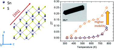
Rod-shaped SnS nanocrystals were synthesized by a facile solvothermal method, which were then compacted by a cold isostatic pressing and rapid annealing process. Two-order higher carrier mobility was achieved in the corresponding bulk samples, leading to over 200% enhancement of thermoelectric figure of merit.


Thermoelectric effects enable direct conversion between thermal and electrical energy, which can be used for both power generation and refrigeration.1 Many recent advances in enhancing the thermoelectric figure of merit (ZT = S2σT/κ) can be attributed to the nanostructuring.2 For example, quantum-confinement effects in the nanomaterials could enhance Seebeck coefficient (S) as well as electrical conductivity (σ), while nanoscale interfaces may reduce thermal conductivity (κ) by affecting the average free path of phonons.3–7 The plumbum or tin chalcogenides, especially PbTe8 and SnSe9, are well known thermoelectric materials with high thermoelectric performance (ZT > 2). As a non-toxic and low-cost member of IV–VI semiconductor, tin sulfide (SnS) has been studied for its optical, physical and electrical properties for a long time.10–12 In addition, the low-dimensional SnS also was investigated as an environment-friendly substitute in the researches on solar cells and the lithium ion batteries.13–16 Meanwhile, many computational studies based on the first-principles calculation were conducted to predict the thermoelectric properties.17,18 Recently, SnS was synthesized by a method combining mechanical alloying (MA) and spark plasma sintering (SPS), which has been revealed to be a promising thermoelectric candidate due to its low thermal conductivity and high thermopower.19,20 Further enhancement in thermoelectric performance can be expected if the electrical conductivity can be improved. It is known that the electrical conductivity of a semiconductor is a result of the product of carrier concentration and mobility. Although increasing the carrier concentration by chemical doping is often employed to improve the electrical conductivity, few studies have been found for the success realized by increasing the carrier mobility, especially in the bulk thermoelectric materials. As an example, this work demonstrates that the ZT of pristine SnS can be greatly enhanced by creating a unique microstructure endowed with high carrier mobility.

In this work, pristine SnS nanorods (NRs) were synthesized by a facile solvothermal (ST) method, which were compacted by cold isostatic pressing and the rapid annealing (RA) process. The resultant bulk materials kept the morphology of nanorods and retained sufficiently high porosity, which is favorable for reducing thermal conductivity. It was interesting that the bulk sample consolidated from the NRs synthesized by solvothermal showed much higher carrier mobility than that from the powders synthesized by mechanic alloying (MA). On the other hand, lower thermal conductivity was obtained due to the porous nanograined structure. As a result, the maximum ZT value was enhanced by >200% from 0.10 to 0.25 at 873 K.

NRs of SnS have been synthesized by mixing SnCl2·2H2O and Na2S·9H2O with a molar ratio of 1[thin space (1/6-em)]:[thin space (1/6-em)]3 in ethanediol without/with dispersants polyethylene glycol (PEG). The mixture was transferred to a solvothermal synthesis reactor made of Teflon at 200 °C for 12 h. After the completion of the reaction, the product was washed with deionized water and ethanol alternately several times and then dried in vacuum at 40 °C for 12 h. After the cold isostatic pressing at 200 MPa, the sample was finally followed by a rapid annealing treatment at 650 °C with a heating rate of 5 °C s−1. For comparison, SnS powders were also synthesized by MA,20 which were subsequently compacted by RA and SPS. Due to the anisotropy of SnS, both the electrical resistivity and thermal conductivity were tested along the same direction. The detailed experimental procedure and cutting direction schematic can be seen in the ESI. XRD patterns of SnS powder synthesized by solvothermal method and the resultant bulk were analyzed with Rietveld refinement method using the MAUD program, and both the observed (Yobs) and calculated (Ycal) patterns are depicted in Fig. 1(a). The refinements carried out with an orthorhombic phase Pbnm (ICSD-650988), indicates that single-phase SnS was successfully synthesized by the solvothermal method. The small Rwp values suggest that the simulated XRD patterns agree well with the measured patterns. Through the solvothermal method with PEG dispersant, well-distributed single crystalline SnS NRs are formed during the solvothermal synthesis, resulting in the hexagonal-like rods, as the SEM image shows in Fig. 1(b). We can clearly see that the nanorods are essentially uniform in both size and morphology when the dispersant was added compared with the powders synthesized by ST without any dispersant (Fig. S2(a)) and the powders synthesized by MA (Fig. S2(b)). After cold isostatic pressing and rapid annealing process, the morphology of hexagonal rods could be correspondingly inheritable, as shown in Fig. 1(c), and the bulk density of the compact sample is 3.5 g cm−3, which is about 70% of the theoretical density. The sufficiently high porosity in bulk sample is favourable for reducing the thermal conductivity. Although the bulk has high porosity and low density, its carrier mobility and electrical conductivity was increased, which will be discussed later.


image file: c6ra06874j-f1.tif
Fig. 1 (a) The observed, calculated, and difference Rietveld refined XRD patterns using MAUD program for the powder synthesized by solvothermal method (ST powder) and the rapid annealed (RA) bulk. The scanning electron microscopy (SEM) images of the (b) ST powder and (c) the fractured surface morphology of the RA bulk.

The morphology and lattice structure of the nanorods were identified by TEM to investigate the growth mechanism of SnS. The micrograph of single SnS NR is shown in Fig. 2(a). The NR has a clear hexagonal shape with a great aspect ratio corresponding to the SEM images. The size of the NRs is about 150 nm × 1000 nm and the thickness is about 30 nm. The selected area electron diffraction (SAED) image, as shown in Fig. 2(b), is observed along the direction vertical to the largest surface of the rod and it qualifies the single crystalline nature of NRs with diffraction spots for the (101), (10−1) and (200) planes. The zonal axis of this diffraction pattern was found to be [010], which was also consistent with the results of the high resolution TEM images, as shown in Fig. 2(c). The crystal structure of SnS is orthorhombic with a Pbnm space group (a = 4.33 ± 0.02 Å, b = 11.19 ± 0.05 Å, and c = 3.98 ± 0.02 Å). Thus the theoretical angle between (101) and (10−1) is 85.17° and the lattice plane spacing of (101) is 2.93 nm, both of which matches with the TEM results. The fastest growth direction of the nanorods was determined to be [101] or [10−1], as shown in Fig. 2(d) and (e). It is easy to tell from the images or to understand that the growth speed along the b-axis direction is the slowest, because SnS has a layered structure perpendicular to the b-axis and the bonding between the layers are primarily van der Waals force. For the SnS NRs synthesized without any dispersant (Fig. S1(b)), non-uniform and irregular tablets were obtained, suggesting that dispersant PEG might inhibit the growth of {101} family of crystal planes.


image file: c6ra06874j-f2.tif
Fig. 2 Electron microscopy patterns of SnS NRs synthesized by solvothermal method. (a) TEM image of single SnS NR, (b) selected area electron diffraction from zonal axis [010] and (c) HRTEM lattice fringe image. The atomistic schematic of the growth mechanism of SnS viewed from different direction (d) [010] and (e) [101].

The thermoelectric properties of SnS compact samples made of ST powder and MA powder were investigated. In Table 1, the measured composition, carrier concentration and mobility of SnS synthesized by different methods are compared. It can be inferred that both the carrier concentration and mobility of ST + RA are higher than that of MA + RA. The mobility of the ST + RA is 33.9 cm2 V−1 s−1, even two-order higher than that of MA + RA, which is only 0.92 cm2 V−1 s−1. Moreover, the mobility of ST + RA is very close to the reported single-crystal value, 80 cm2 V−1 s−1 at room temperature12. There are mainly two reasons why the ST + RA sample has a higher carrier mobility. Firstly, the bulk is compacted by the single crystal nanorods which have less defects and the more exact stoichiometric composition (Table 1) than the powder synthesized by MA. Defects which can increase the scattering of carriers, were introduced more easily and the raw materials may be consumed during the MA process. Secondly, the rod-shaped nanocrystal has a specific orientation that is beneficial to the increase of carrier mobility. The morphological shortest direction is along the b-axis, which has the lowest carrier mobility. Thus the carriers have more possibilities to move along the directions with higher mobility.

Table 1 The measured composition, carrier concentration and mobility of SnS synthesized by different methods
Synthesis method Measured composition nH, cm−3 μ, cm2 V−1 s−1 Density, g cm−3
Sn S
ST + RA 1 1.03 2.83 × 10¹⁶ 33.9 3.42
MA + RA 1 1.06 1.14 × 10¹⁶ 0.92 3.49


The higher carrier mobility results in the significant decrease of electrical resistivity from 100–1000 of the MA samples to around 1 Ω cm−1 of the ST + RA one at room temperature as shown in Fig. 3(a). The upturn of electrical resistivity observed in the ST + RA and MA + RA samples between 500 K and 700 K is probably due to the energy barrier scattering, because in rapid annealing process the samples were sintered without any pressure and the bonding among the grains is weaker than the SPS one. The energy barrier scattering could affect the mobility as the following relationship,

μAT−1/2eEB/T
where A is constant, EB is the barrier energy, both of them can be simulated in different systems. With the increasing temperature, the carrier mobility at first increases then decreases and the maximum was obtained around 500 K, leading to the upturn of electrical resistivity at 500 K. This phenomenon was also observed in SnSe compound.21 The reduced resistivity is mainly due to the high carrier mobility in the ST + RA sample. This result is very interesting. Generally, increasing carrier concentration by doping is a major method to increase electrical conductivity, but it is also accompanied by an unavoidable decrease of Seebeck coefficient. Although the electrical resistivity decreases significantly, the Seebeck coefficient decreases slightly due to the higher carrier concentration of ST + RA sample and all the Seebeck coefficients of SnS samples are above 350 μV K−1, as Fig. 3(b) shows. In addition, the scattering mechanism was complicated in SnS samples and the scattering mechanism could affect the Seebeck coefficient. The MA sample has more defects so that it has larger Seebeck coefficient. Although the reason why the SPS sample has a larger coefficient than the RA sample is not clear, the scattering mechanism should be the critical point. Thermal conductivity of the samples consolidated by the RA could reach a fairly low value of 0.35 W m−1 K−1 at 873 K as a result of its sufficiently high porosity. Thermal conductivity of the MA + SPS sample in this work is slightly higher if compared with our previous work,20 which is probably due to the batch differences including raw materials and the actual SPS temperature. Considering the measurement uncertainty, this result is also acceptable. The better electrical property and lower thermal conductivity contribute to the enhancement of ZT value for the ST + RA sample, achieving 0.25 at 773 K, which is improved by 200% compared with the undoped sample fabricated by the MA + SPS method. Further enhancement can be expected if the strategy proposed in this study is applied to Ag-doped SnS with optimized carrier concentrations.


image file: c6ra06874j-f3.tif
Fig. 3 Temperature dependence of (a) resistivity (b) Seebeck coefficient (c) thermal conductivity (d) ZT and of the bulk samples synthesized by ST and RA, MA and RA, MA and SPS, respectively.

Conclusions

Single-crystalline SnS nanorods were synthesized by a facile solvothermal method and the growth mechanism was also investigated. The SnS bulk was then prepared by isostatic pressing and rapid thermal annealing method. The carrier mobility reaches above 30 cm2 V−1 s−1, which is nearly two-order higher compared with the MA sample. The higher carrier mobility contributed to a much lower electrical resistivity, and consequently high Seebeck coefficient was retained. Also benefited from the low thermal conductivity reduced by porosity, the thermoelectric performance was significantly enhanced over 200% in the porous compacts of SnS nanorods. This work demonstrates a new strategy for thermoelectric performance enhancement by increasing carrier mobility, which improves electrical conductivity but keeping high Seebeck coefficient.

Acknowledgements

This work was supported by the National Natural Science Foundation of China (Grants No. 51172121, 11474176) and the National Basic Research Program of China (Grant No. 2013CB632503).

Notes and references

  1. L. E. Bell, Science, 2008, 321, 1457–1461 CrossRef CAS PubMed.
  2. M. G. Kanatzidis, Chem. Mater., 2010, 22, 648–659 CrossRef CAS.
  3. C. J. Vineis, A. Shakouri, A. Majumdar and M. G. Kanatzidis, Adv. Mater., 2010, 22, 3970–3980 CrossRef CAS PubMed.
  4. Y. Lan, A. J. Minnich, G. Chen and Z. Ren, Adv. Funct. Mater., 2010, 20, 357–376 CrossRef CAS.
  5. H. Yang, L. A. Jauregui, G. Zhang, Y. P. Chen and Y. Wu, Nano Lett., 2012, 12, 540–545 CrossRef CAS PubMed.
  6. J. Yang, H.-L. Yip and A. K. Y. Jen, Adv. Energy Mater., 2013, 3, 549–565 CrossRef CAS.
  7. C. Ou, J. Hou, T.-R. Wei, B. Jiang, S. Jiao, J.-F. Li and H. Zhu, NPG Asia Mater., 2015, 7, e182 CrossRef.
  8. K. Biswas, J. He, I. D. Blum, C. I. Wu, T. P. Hogan, D. N. Seidman, V. P. Dravid and M. G. Kanatzidis, Nature, 2012, 489, 414–418 CrossRef CAS PubMed.
  9. L. D. Zhao, S. H. Lo, Y. Zhang, H. Sun, G. Tan, C. Uher, C. Wolverton, V. P. Dravid and M. G. Kanatzidis, Nature, 2014, 508, 373–377 CrossRef CAS PubMed.
  10. H. R. Chandrasekhar, R. G. Humphreys, U. Zwick and M. Cardona, Phys. Rev. B: Solid State, 1977, 15, 2177–2183 CrossRef CAS.
  11. M. M. Nassary, J. Alloys Compd., 2005, 398, 21–25 CrossRef CAS.
  12. W. Albers, C. Haas, H. J. Vink and J. D. Wasscher, J. Appl. Phys., 1961, 32, 2220 CrossRef CAS.
  13. H. Liu, Y. Liu, Z. Wang and P. He, Nanotechnology, 2010, 21, 105707 CrossRef PubMed.
  14. D. D. Vaughn, O. D. Hentz, S. Chen, D. Wang and R. E. Schaak, Chem. Commun., 2012, 48, 5608–5610 RSC.
  15. A. M. Tripathi and S. Mitra, RSC Adv., 2014, 4, 10358 RSC.
  16. T. Rath, L. Gury, I. Sánchez-Molina, L. Martíneza and S. A. Haque, Chem. Commun., 2015, 51, 10198–10201 RSC.
  17. D. Parker and D. J. Singh, J. Appl. Phys., 2010, 108, 083712 CrossRef.
  18. S. Bhattacharya, N. S. Gunda, R. Stern, S. Jacobs, R. Chmielowski, G. Dennler and G. K. Madsen, Phys. Chem. Chem. Phys., 2015, 17, 9161–9166 RSC.
  19. Q. Tan and J.-F. Li, J. Electron. Mater., 2014, 43, 2435–2439 CrossRef CAS.
  20. Q. Tan, L.-D. Zhao, J.-F. Li, C.-F. Wu, T.-R. Wei, Z.-B. Xing and M. G. Kanatzidis, J. Mater. Chem. A, 2014, 2, 17302–17306 CAS.
  21. T.-R. Wei, C.-F. Wu, X. Zhang, Q. Tan, L. Sun, Y. Pan and J.-F. Li, Phys. Chem. Chem. Phys., 2015, 17, 30102–30109 RSC.

Footnote

Electronic supplementary information (ESI) available: Details to performed experiments and characterisation method; supplementary morphology. See DOI: 10.1039/c6ra06874j

This journal is © The Royal Society of Chemistry 2016