Ultrathin tandem-plasmonic photovoltaic structures for synergistically enhanced light absorption

Jafar Poursafara, Mohammadreza Kolahdouz*a, Ebrahim Asl-Soleimania and Saeed Golmohammadib
aSchool of Electrical and Computer Engineering, University of Tehran, Tehran, Iran. E-mail: Kolahdouz@ut.ac.ir
bSchool of Engineering-Emerging Technology, University of Tabriz, Tabriz, Iran

Received 12th March 2016 , Accepted 23rd May 2016

First published on 25th May 2016


Abstract

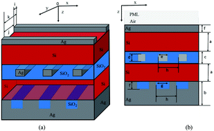
Recently, plasmonic nanostructures have been playing a key role in enhancing the optical absorption in thin film solar cells, which are poor absorbers due to their decreased optical travelling path length. Here, we have proposed and simulated a tandem ultra-thin silicon solar cell, in which each layer is integrated with metal nanostructures, using the FDTD method. The Si layers are disconnected via a SiO2 layer with embedded Ag strips. The surface of the top Si layer and the underside of the bottom Si layer are connected to each other using contacts from a Ag periodic array nanostructure. The simulation results have demonstrated that the proposed structure has a synergistic effect on light absorption and gives rise to a 172% light absorption enhancement and 139% short-circuit current density enhancement over the whole usable solar spectrum, compared with the one layer bared structure.


1. Introduction

Photovoltaic devices suffer from two major problems: one is low conversion efficiency and the other is high production cost. Materials and processing represent a large fraction of the expenses. About 40% of the final module price of bulk crystalline silicon solar cells comes from the silicon materials and its processing costs.1,2 Recently, thin film solar cells with an active layer thickness of about 1 to 2 μm were desired as a way to reduce the material costs. Beside the low manufacturing costs for bulk recombination-dominated semiconductors, thin-film solar cells can also reduce carrier recombination rate and improve the carrier collection efficiency which results in a better overall solar cell efficiency. However, one disadvantage of all thin film solar cells is weak absorption at the wavelengths near to the electronic bandgap of the semiconductor, due to the reduced absorber thickness. Therefore, light trapping schemes are needed for the design of ultrathin solar cells to enhance light absorption.1,3–5

In the past few years, many light trapping methods have been proposed for photovoltaic applications. Conventional macroscopic surface textures are not suitable for thin film photovoltaics, because the cell thickness is comparable to or smaller than the macroscopic textures. Nowadays, metallic nanostructures engineered within the solar cell geometry have been proposed as an alternative method to improve light trapping.6–9 These subwavelength nanostructures strongly interact with sunlight and can redirect incident light into the ultrathin active layers, and thereby improve light absorption. There are two different schemes for the integration of plasmonic nanostructures. Firstly, metal nanoparticles placed on the top surface of the active layer can act as scattering elements to redirect the incident sunlight into the active layer and thereby, if the absorber layer is instead a thin film, can effectively increase the optical path length inside the absorber layer.10–13 A 1.25 μm thick silicon-on-insulator solar cell with metal nanoparticles placed on the top surface has been reported experimentally, and demonstrated over 30% photocurrent enhancement.14 Secondly, the metallic patterned back contact is decorated directly, without introducing any extra metal features. Sunlight couples from these patterned back contacts into the guided modes of the absorber layer, as well as to surface plasmon polariton (SPP) modes that propagate along the metal/semiconductor interface. A thin film solar cell, by utilizing this approach, shows about 30% light absorption enhancement.15

2. Structure design and simulation method

We solved Maxwell’s wave equations to extract the performance of the cell using the finite-difference time-domain (FDTD) method. The structures were illuminated from the top surface at normal incidence with both transverse magnetic (TM) and transverse electric (TE) plane polarized light, in regards to the fact that the approximate solar spectrum at Earth’s surface is about a 50% contribution from each polarization. The boundary conditions were set to the perfectly matched layers (PMLs) in the propagation direction. Other FDTD simulation parameters are shown in Table 1.
Table 1 Finite-difference time-domain method parameters
Min mesh step (nm) 0.25
Time step dt (fs) 0.075822
Simulation time (fs) 1000
Min sampling per cycle 2
Spatial cell size dx (nm) 5
Spatial cell size dy (nm) 5
Spatial cell size dz (nm) 3


The complex Poynting vector is:

 
[P with combining right harpoon above (vector)] = [E with combining right harpoon above (vector)](w) × [H with combining right harpoon above (vector)]∗(w) (1)
where [E with combining right harpoon above (vector)](w) and [H with combining right harpoon above (vector)]∗(w) are the electric and magnetic fields (average of the two polarizations). The power flow in a particular direction can be obtained using eqn (1). As is obvious, the power of the propagating wave is only proportional to the real part of the Poynting vector, which is related to the conservation of energy for the time averaged quantities.14,16–18 So, the time-averaged power flow across a surface is given by:
 
image file: c6ra06586d-t1.tif(2)

The 1/2 factor in eqn (2) is related to the time-averaging of the clockwise fields. For obtaining the transmitted power (T(w)) the imaginary part of the Poynting vector is not needed, because it has a relation with the non-propagating reactive or stored energy. Consequently, the transmitted power (T(w)) can be calculated by considering the real time-averaged power variations along the x and y axes for the monitor and electric field source, respectively:

 
image file: c6ra06586d-t2.tif(3)

Now, all related quantities such as absorption, reflection, etc. were obtained from the transmitted power plane.18 For ultrathin Si solar cells where the Si layer thickness is remarkably smaller than the diffusion length, it is fairly reasonable to suppose that all photo-generated carriers can be collected at the electrodes, since the diffusion length of crystalline silicon is around 100 μm. On that account, if every absorbed photon generates an electron–hole pair, Jsc (the short-circuit current density) becomes:

 
image file: c6ra06586d-t3.tif(4)
where q is the charge of an electron, I(λ) is the solar irradiance, and R(λ) is the spectral response of the cell. The short-circuit current densities are weighted by the terrestrial solar spectrum (AM 1.5 solar spectrum).16,19 The absorption function (φ(λ)) is defined as the ratio of light absorption power inside the Si layers to the incident light power. To obtain the promising results from the simulation, the materials’ (silver, silicon dioxide and crystalline silicon) parameters were extracted from previously published experimental data.20–22

The schematic of the designed solar cell is illustrated in Fig. 1a and b with the defined structural parameters. As is shown in this figure, the structure consists of a gravitated Ag substrate, a bottom Si absorbing layer, a dielectric spacer layer of SiO2 with Ag stripes embedded inside, a top Si absorbing layer, and a periodic array of Ag strips which is connected to the Ag substrate. The free line spaces in the Ag substrate are filled with SiO2. In all of the calculations, the parameters and dimensions were set to a fixed set of numbers. As indicated in Fig. 1, the dimensions in nanometers are a = 80, b = 160, c = 45, d = 35, e = 50, f = 40, g = 150, h = 225, i = 100, j = 500, and k = 600. The structure is periodic in two directions, x and y, and h and k are 225 nm in the x-direction and k = 600 nm in the y-direction (structure C). A simple plasmonic structure with the same parameters and dimensions as structure C was simulated for comparison with the proposed structure (structure B). The bared structure was also considered as a Si layer deposited on an Ag substrate (structure A).


image file: c6ra06586d-f1.tif
Fig. 1 (a) Schematic diagram of the proposed double layer plasmonic solar cell structure (structure C). (b) Side view of structure C.

3. Results and discussion

Fig. 2a shows the absorption efficiency spectra for the bared thin film solar cell that is being used as the reference. As shown in this figure, there are two absorption peaks that are related to the enhanced magnetic fields inside the Si layer, originating from the Fabry–Perot (FP) cavity resonance.23 If the incidence wavelengths and absorbing layer thickness satisfy the resonance condition, the FP resonance occurs which means that the FP resonance can be modified by altering the thicknesses, in a way that by increasing the absorbing layer thickness, the FP cavity resonances shift to longer wavelengths. Fig. 2b and c show the absorption efficiency spectra for structures B and C. In these cases, there are multiple absorption peaks that are related to the excited multiple resonance modes. By comparing the absorption efficiencies, it is obvious that the presence of the metal nanostructures in the single and double layer solar cells leads to multiple strong enhanced absorption bands. In addition, the absorption enhancement peaks occur at the wavelengths where the radiation intensity of the solar spectrum is high.
image file: c6ra06586d-f2.tif
Fig. 2 (a) The absorption spectrum for structure A. (b) The absorption spectrum for structure B. (c) The absorption spectrum for structure C. (d) Wavelength of the absorption peak 3 versus the periodicity in the y-direction for the proposed structure. The insets show the structures.

3.1. Absorption enhancement mechanisms

The proposed structure (structure C) has periodicity in both the x and y directions and four absorption peaks (Fig. 2c) while the bare structure has two (Fig. 2a). In order to explore the mechanisms of the absorption enhancement peaks and their relation with the periodicity, the normalized magnetic field distributions and absorption map (φ(λ)) versus the period of unit cells were investigated, as shown in Fig. 3 and 4, respectively. Fig. 4 represents the full-field simulation results with the corresponding absorption wavelengths and periods. For considering the effect of periodicity, the x-direction unit cell period has been changed while the y-direction unit cell period was kept constant to a certain number and vice versa. As shown in Fig. 4d–f, the y-direction unit cell period has been varied from 550 to 650 nm. Since the period in the y-direction is much longer than in the x-direction, the effect of the y-direction period on the absorption peak wavelengths and power is not noticeable (Fig. 4d–f).
image file: c6ra06586d-f3.tif
Fig. 3 The normalized magnetic field distribution for the incident TM polarized light at wavelengths of (a) 540 nm, (b) 630 nm, and (c) 980 nm.

image file: c6ra06586d-f4.tif
Fig. 4 The normalized map of the absorption function (φ(λ)) spectra vs. the wavelengths for the proposed structure for the incident TM polarized light (a–c for periods in the x-direction and d–f for periods in the y-direction; the dashed lines are for the selected periods).

We can relate the absorption peak “1” to the slab waveguide modes which depend on the absorber layer thickness. The wavelength of the slab waveguide modes is around 540 nm and its corresponding magnetic field distribution is shown in Fig. 3. As illustrated in this figure, the magnetic fields are confined between the two active layers.24–30 Fig. 4a clearly exhibits that there is no relation between the slab waveguide modes and the periods. The magnetic field distributions of absorption peak “2” which has a wavelength of around 630 nm is illustrated in Fig. 3. It can be clearly seen that the magnetic fields are trapped into both Si layers, especially around the metal strips which can be attributed to the localized surface plasmon resonance mode (LSPR) of the metal strips, thereby the related absorption peak wavelength mainly depends on the size of the metal nanostructures and secondly on their periodicity. According to Fig. 4b, the absorption peak variations around 630 nm generated by changing the periodicity of the structure, are not significant. The thick metallic nanostripes act as a mirror and cast a shadow on the absorber layers, whereas the thin nanostripes scatter the sunlight very weakly and do not contribute to the absorption enhancement, and consequently the size and period of these nanostripes have optimum values and their own complication.27,31–33

It can be clearly seen that the magnetic field at the metal/semiconductor interface (SPP mode) is high and decays sharply moving away from the interface. This can be confirmed by looking at the magnetic field distributions of the last absorption peak “3” in Fig. 3. The related wavelength of the SPP mode that happens at the metal/semiconductor interface is around 980 nm and can be modified by changing the period of the metal stripes (Fig. 4c).13,34,35 To show the y-direction period effect on the wavelength of the absorption peak when it is comparable with the x-direction, small periodicity in the y-direction is considered, as shown in Fig. 2d, and the period of the metal stripes defines the absorption peak wavelength. It is obvious that for photovoltaic applications, the best absorption peaks are located where the solar spectrum intensity is high, thereby the wavelength of absorption peaks in this structure can be modified by changing the period and size of the metal strips.32 The absorption peaks of structure B, which are shown in Fig. 2b, are the same as for structure C, but they are insignificant.

The transmission and reflection of the three mentioned structures are plotted in Fig. 5a and b. It is obvious from Fig. 2 and 5 that the average transmission and absorption of the one layer plasmonic structure is more than the bared structure. This can be elucidated by the fact that the reflecting light intensity in structures B and C is much less than in the bared structure, as is obvious from Fig. 5b. It should be noted that the utilization of the double absorber layer can achieve the desired synergistic effect on the light absorption, in such a way that the absorption enhancement significantly increases from 34% for the plasmonic single layer to 172% for the tandem-plasmonic structure. The absorption enhancement gives rise to a high short-circuit current density. For the AM 1.5 solar spectrum, the short-circuit current densities become 4.96, 6.29 and 11.46 (mA cm−2) for structures A, B and C, respectively. The current density enhancement for structure B is 26.81% and it is 131% for structure C with respect to the reference bared structure.


image file: c6ra06586d-f5.tif
Fig. 5 (a) Transmission and (b) reflection for the three different structures: structure A (solid), structure B (dash) and structure C (dot).

4. Conclusion

In summary, a Si tandem solar cell structure was introduced and the light absorption properties of the structure were discussed in detail using the FDTD method. The proposed structure was compared with bared and plasmonic structures, and the results showed 172% and 139% light absorption and short-circuit current density efficiency enhancement compared to the bare structure, respectively. The simulated optical field distributions in the device were investigated and the related absorption enhancement mechanisms were thoroughly discussed. The obtained results propose a promising way to reach high efficiency in thin film solar cells.

References

  1. M. A. Green, Prog. Photovoltaics, 2002, 10, 235–241 CAS.
  2. M. L. Brongersma, Y. Cui and S. Fan, Nat. Mater., 2014, 13, 451–460 CrossRef CAS PubMed.
  3. A. Shah, P. Torres, R. Tscharner, N. Wyrsch and H. Keppner, Science, 1999, 285, 692–698 CrossRef CAS PubMed.
  4. C. Tang, Z. Yan, Q. Wang, J. Chen, M. Zhu, B. Liu, F. Liu and C. Sui, RSC Adv., 2015, 5, 81866–81874 RSC.
  5. X. Zhao, C. Duan, Z. Liang and H. Shen, RSC Adv., 2014, 4, 13757–13763 RSC.
  6. K. R. Catchpole and A. Polman, Opt. Express, 2008, 16, 21793–21800 CrossRef CAS PubMed.
  7. D. M. Schaadt, B. Feng and E. T. Yu, Appl. Phys. Lett., 2005, 86, 063106 CrossRef.
  8. H. Tan, R. Santbergen, A. H. M. Smets and M. Zeman, Nano Lett., 2012, 12, 4070–4076 CrossRef CAS PubMed.
  9. H.-H. Hsieh, Y.-M. Sung, F.-C. Hsu, K.-J. Hsiao, Y.-J. Lee and Y.-F. Chen, RSC Adv., 2015, 5, 1549–1556 RSC.
  10. D. Qu, F. Liu, Y. Huang, W. Xie and Q. Xu, Opt. Express, 2011, 19, 24795–24803 CrossRef CAS PubMed.
  11. C. Hägglund, M. Zäch, G. Petersson and B. Kasemo, Appl. Phys. Lett., 2008, 92, 013113 CrossRef.
  12. S. Pillai, K. R. Catchpole, T. Trupke and M. A. Green, J. Appl. Phys., 2007, 101, 093105 CrossRef.
  13. K. R. Catchpole and A. Polman, Appl. Phys. Lett., 2008, 93, 191113 CrossRef.
  14. R. A. Pala, J. White, E. Barnard, J. Liu and M. L. Brongersma, Adv. Mater., 2009, 21, 3504–3509 CrossRef CAS.
  15. R. Biswas and D. Zhou, Phys. Status Solidi, 2010, 207, 667–670 CrossRef CAS.
  16. M. A. Awal, Z. Ahmed and M. A. Talukder, J. Appl. Phys., 2015, 117, 193101 CrossRef.
  17. L.-H. Zhu, M.-R. Shao, R.-W. Peng, R.-H. Fan, X.-R. Huang and M. Wang, Opt. Express, 2013, 21, A313–A323 CrossRef CAS PubMed.
  18. A. Ahmadivand, S. Golmohammadi and A. Rostami, Appl. Opt., 2012, 51, 2784–2793 CrossRef CAS PubMed.
  19. A. Ahmadivand and N. Pala, J. Opt. Soc. Am. A, 2015, 32, 204–212 CrossRef CAS PubMed.
  20. J. Humlíček, F. Lukeš and E. Schmidt, in Handbook of Optical Constants of Solids, ed. E. D. Palik, Academic Press, Boston, 1998, pp. 607–636 Search PubMed.
  21. C. Schinke, P. Christian Peest, J. Schmidt, R. Brendel, K. Bothe, M. R. Vogt, I. Kröger, S. Winter, A. Schirmacher, S. Lim, H. T. Nguyen and D. MacDonald, AIP Adv., 2015, 5, 067168 CrossRef.
  22. D. W. Lynch and W. R. Hunter, Handbook of Optical Constants of Solids, Elsevier, 1997 Search PubMed.
  23. A. W. Snyder and J. D. Love, Optical Waveguide Theory, Springer, US, Boston, MA, 1984 Search PubMed.
  24. V. E. Ferry, L. A. Sweatlock, D. Pacifici and H. A. Atwater, Nano Lett., 2008, 8, 4391–4397 CrossRef CAS PubMed.
  25. R. B. Dunbar, T. Pfadler and L. Schmidt-Mende, Opt. Express, 2012, 20, A177–A189 CrossRef CAS PubMed.
  26. Y. A. Akimov, W. S. Koh and K. Ostrikov, Opt. Express, 2009, 17, 10195–10205 CrossRef CAS PubMed.
  27. W. Bai, Q. Gan, G. Song, L. Chen, Z. Kafafi and F. Bartoli, Opt. Express, 2010, 18, A620–A630 CrossRef CAS PubMed.
  28. E. Battal, T. A. Yogurt, L. E. Aygun and A. K. Okyay, Opt. Express, 2012, 20, 9458–9464 CrossRef CAS PubMed.
  29. J. Y. Chen and K. W. Sun, Sol. Energy Mater. Sol. Cells, 2010, 94, 629–633 CrossRef CAS.
  30. P. B. Johnson and R. W. Christy, Phys. Rev. B: Solid State, 1972, 6, 4370–4379 CrossRef CAS.
  31. P. Ding, E. Liang, G. Cai, W. Hu, C. Fan and Q. Xue, J. Opt., 2011, 13, 75005 CrossRef.
  32. Y. Xuan, H. Duan and Q. Li, RSC Adv., 2014, 4, 16206–16213 RSC.
  33. S. J. Lee, J.-Y. Kim, A. R. Bin Mohd Yusoff and J. Jang, RSC Adv., 2015, 5, 23892–23899 RSC.
  34. N. Papanikolaou, Phys. Rev. B: Condens. Matter Mater. Phys., 2007, 75, 235426 CrossRef.
  35. N. Zhou, V. Lopez-Puente, Q. Wang, L. Polavarapu, I. Pastoriza-Santos and Q.-H. Xu, RSC Adv., 2015, 5, 29076–29097 RSC.

This journal is © The Royal Society of Chemistry 2016
Click here to see how this site uses Cookies. View our privacy policy here.