Daniel E. Martínez-Tong*a,
Gabin Gbabodeb,
Christian Ruziéc,
Basab Chattopadhyayc,
Guillaume Schweicher‡
c,
Alan R. Kennedyd,
Yves H. Geertsc and
Michele Sferrazzaa
aDépartement de Physique, Faculté des Sciences, Université Libre de Bruxelles, 1050 Brussels, Belgium. E-mail: danmarti@ulb.ac.be
bNormandie Université, Laboratoire SMS EA 3233, Université de Rouen, F-76821 Mont Saint Aignan, France
cLaboratoire de Chimie des Polymères, Faculté des Sciences, Université Libre de Bruxelles, 1050 Brussels, Belgium
dDepartment of Pure and Applied Chemistry, University of Strathclyde, 295 Cathedral Street, Glasgow G1 1XL, Scotland, UK
First published on 20th April 2016
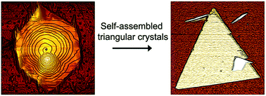
Organic semiconducting materials in confined geometries present interesting properties connected to change or the coexistence of molecular organizations, depending on their characteristic scales. In this work the preparation and structural characterization of self-assembled π-conjugated organic nanoplates of 2,7-diperfluorohexyl-[1]benzothieno[3,2,b]benzothiophene are studied. These nanostructures were prepared by spin coating, implementing a fast precipitation method. We observed an evolution of the nanostructures from hexagonal towards triangular nanoplates, possibly driven by enhanced solvent/molecule interactions, and accompanied by the formation of a new polymorph.
Among confined geometries, special attention has been drawn towards two-dimensional materials, i.e. systems where only one of its geometrical dimensions is in the nanoscale regime, having thus large specific surface areas.6 One issue that is relevant when transitioning from bulk towards a confined level is related to the structural organization of the molecules. By decreasing the characteristic thickness, it has been observed a change of the crystal organization compared to the bulk one7 or a coexistence of crystalline phases8 (polymorphism). The crystal structure of the material may also evolve depending on different parameters, such as thickness, aging of the film or solvent annealing, tuning then the crystal organization from metastable phases to thermodynamically stable phases.3,9
Soft materials are the subject of intense research due to their self-assembly properties, structural control and flexibility, diversity of fabrication approaches, etc.6 In this area, it is possible to find bidimensional systems such as nanoplates: materials which are typically nanoscale in one dimension, yet microscale in the other two,10–12 and that, contrary to thin films, do not span large surface areas but are distributed as features, generally on a supporting substrate. The idea behind nanoplates consists in developing independent nanostructures with well controlled and tunable geometries,13 such as squares,14 hexagons15 and triangles,16 which could lead to different specific applications in organic-based technologies. For example, it is possible to prepare nanoplates of organic molecules with a π-conjugated (hetero)aromatic backbone.17 Typically, these structures are stabilized by the π–π interactions within self-assembled stacked lamellae1,2 which in turn provide anisotropic channels for the transportation of charge carriers and efficient light interaction.13 Following these ideas, in this work we present the preparation and structural characterization of self-assembled π-conjugated organic nanoplates of 2,7-diperfluorohexyl-[1]benzothieno[3,2,b]benzothiophene (F13C6-BTBT-C6F13). By means of a fast precipitation protocol we have prepared different nanostructures, by changing the solution concentration. We observed an evolution from hexagonal nanoplates towards equilateral triangles which lead to a change in the crystalline structure of the material.
A mixture of 2,7-diiodo-[1]benzothieno[3,2-b][1]benzothiophene (492 mg, 1 mmol), Cu powder (572 mg, 9 mmol), and perfluorohexyliodide (1.08 mL, 5 mmol) in anhydrous DMSO (20 mL) in a Schlenk flask was degassed by 2 “freeze–pump–thaw” cycles. The Schlenk flask was filled with Ar, and sealed. The mixture was heated for 2 days at 130 °C. After cooling to room temperature, water (50 mL) was added. The resulting precipitate was filtrated, washed with water, and methanol. The dried residue was dissolved in boiling tetrachloroethane and subjected to short silica filtration to afford after evaporation and recrystallization in tetrachloroethane a white powder (682 mg, 78%). 1H NMR (400 MHz, C2D2Cl4, 363 K) δ = 8.26 (s, 2H), 8.10 (d, J = 8.1 Hz, 2H), 7.75 (dd, J = 8.1 and 2.1 Hz, 2H); 19F NMR (376 MHz, C2D2Cl4, 363 K) δ = −81.3 (m, 3F), −109.6 (m, 2F), −121.5 (m, 4F), −122.9 (m, 2F), −126.2 (m, 2F). HRMS (MALDI-HRMS): m/z calculated for C26H6F26S2: 875.9496; found 875.9468.
F13C6-BTBT-C6F13 | |
---|---|
Empirical formula | C26H6F26S2 |
Formula weight | 876.43 Da |
Crystal system | Monoclinic |
Space group | C2/c |
a, b, c [Å] | 53.119(8), 5.8356(6), 9.0022(13) |
β [°] | 95.343(15) |
Volume [Å3] | 2778.4(6) |
Z, Z′ | 4, 0.5 |
Density [g cm−3] | 2.095 |
Crystal size [mm3] | 0.12 × 0.10 × 0.03 |
Reflections collected | 9621 |
Independent reflections | 2742, [R(int) = 0.0682] |
Goodness-of-fit on F2 | 1.080 |
Final R indices [I > 2sigma(I)] | R1 = 0.0628, wR2 = 0.1630 |
R indices (all data) | R1 = 0.0995, wR2 = 0.2022 |
Hirshfeld surfaces20,21 and the associated fingerprint plots22 were calculated using Crystal Explorer23 which accepts a structure input file in the CIF format. Bond lengths to hydrogen atoms were set to typical neutron values (C–H = 1.083 Å). For each point on the Hirshfeld isosurface, two distances de, the distance from the point to the nearest nucleus external to the surface, and di, the distance to the nearest nucleus internal to the surface, are defined. The normalized contact distance (dnorm) based on de and di is given by:
![]() | ||
Fig. 2 (a) Molecular structure of F13C6-BTBT-C6F13 along with the unsubstituted BTBT30 is presented for comparison. (b) Side view of the crystal packing. (c) Lattice parameters and top view of the lamellar herringbone packing structure. |
In order to have a clear quantitative and visual insight of the intermolecular interactions, the Hirshfeld surfaces of the unsubstituted BTBT, C8-BTBT-C8 and F13C6-BTBT-C6F13 is presented in Fig. S1 (ESI material†) showing surfaces that have been mapped over a dnorm range of −0.5 to 1.5 Å. The dominant interactions can be seen in the Hirshfeld surfaces (Fig. S1†) as the bright red areas corresponding to the C–H⋯π interactions, and C–H⋯F and F⋯F contacts in F13C6-BTBT-C6F13. A look at the 2D fingerprint plots (Fig. 4a) reveals that fluorination of the alkyl side chains leads to a different packing environment although all three compounds exhibit a similar herringbone motif. The C–H⋯π hydrogen bonds in the unsubstituted BTBT, C8-BTBT-C8 and F13C6-BTBT-C6F13 are well manifested and appear as a pair of wings of almost equal lengths in the (di, de) regions (1.7 Å, 1.1 Å) and (1.1 Å, 1.7 Å). For F13C6-BTBT-C6F13, the C–H⋯F interactions appear as sharp spikes in the (di, de) regions (1.4 Å, 1.1 Å) and (1.1 Å, 1.4 Å). Moreover, the F⋯F interactions in F13C6-BTBT-C6F13 contributes to the spike at di = de = 1.4 Å. This is in contrast to the unsubstituted BTBT and C8-BTBT-C8 where the spike at di = de = 1.2 Å is a consequence of the short intermolecular H⋯H contacts. Fig. 4b highlights the relative contributions of different intermolecular interactions to the Hirshfeld surface area. The quantitative analysis shows that C⋯H contacts corresponding to C–H⋯π interactions account for 35.3% in the unsubstituted BTBT and 14.9% in C8-BTBT-C8 while in F13C6-BTBT-C6F13 it is only 12.3% of the Hirshfeld surface area. In F13C6-BTBT-C6F13 the absence of hydrogen atoms among the lateral chains reduces considerably the impact of the hydrogen interactions and leads to a packing dominated by fluorine interactions as can be observed by the drastic decrease of the H⋯H and C⋯H interactions (15.4% in total) and huge contributions of the F⋯F, F⋯C and F⋯H interactions (71.6% in total).
![]() | ||
Fig. 4 (a) Fingerprint plots and (b) relative contributions to the Hirshfeld surface areas for the various intermolecular contacts for BTBT core, C8-BTBT-C8 and F13C6-BTBT-C6F13. |
Concentrated samples (10 mg mL−1 and 5 mg mL−1) show the development of polygonal nanoplates randomly distributed on the silicon surface. Specifically, in Fig. 5a, the 10 mg mL−1 preparation shows features spanning areas around 5 μm2 and having heights from 200–500 nm (at their highest point, respect to the silicon). In most of the cases, these features have 5, 6 to 8 lateral sides, mostly resembling the general shape of hexagons. Also, we observe elongated walls apparently emerging from the edge of the nanoplates, as shown in Fig. 5b. These features are likely related to possible vestiges of the nanoplates' formation process. As solution concentration was decreased to 5 mg mL−1, changes in the shape and size of the molecular organization are observed. In this case several structures show a (almost) hexagonal geometry, with areas between 1 and 2 μm2 and heights close to 200 nm (please refer to Fig. 5d). The transition toward more defined structures, as well as the decrease in their characteristics dimensions, can be related to the availability of material at this concentration: as solution gets diluted, less material can be processed into the final nanostructures.
Considering the bulk crystal structure presented in the previous section, we have calculated the expected crystal growth morphology using the Morphology module implemented in Materials Studio software (see Experimental section). In consistency with the AFM observations, the calculated morphology is octagonal (see Fig. S2†) with the large top and bottom surfaces corresponding to the {200} faces, that is, with the molecular axis perpendicular to these faces. However, hexagonal shaped crystals are more observed by AFM. This is not really an inconsistency with the calculation, as the latter does not take into account solvent–solute interactions that might inhibit the growth of certain crystal faces,16 resulting in an observed crystal morphology slightly different from the theoretical one. For example, if we suppose that the {110} or {002} faces are totally absent from the theoretical morphology, we will end up with a hexagonal crystal morphology akin to that observed by AFM. The relevant data from the calculations are gathered in Table 2. There we present the interreticular distance (dhkl) of the (hkl) reticular planes and the attachment energy (Eatt) and facet coverage percentage of the corresponding {hkl} crystal faces.31 The lower the attachment energy of a given face (in absolute values), the lower is its growth rate and consequently the higher should be its area in the final crystal morphology.
hkl | dhkl (Å) | Eatt (kJ mol−1) | % total facet area |
---|---|---|---|
{2 0 0} | 26.4 | −17 | 78.0 |
{1 1 1} | 4.8 | −118 | 9.3 |
{0 0 2} | 4.5 | −135 | 5.7 |
{1 1 0} | 5.8 | −116 | 4.3 |
{1 1 −1} | 4.9 | −121 | 2.7 |
We have performed AFM scans on the top surface of the nanoplates, presented in Fig. 5c and f. Here, it is possible to observe the development of spiral staircase-like structures, formed by the arrangement of step-distributed terraces, with cores at the center of the nanoplates. As detailed in Fig. 5f, the spirals can grow either left- or right-handed, and more than one core might exist within the same surface. As previously reported for other nanostructures with comparable geometries,10 our nanoplates show interference patterns when the sample is illuminated under simple bright-field optical microscopy, revealing the geometry and thickness variation of the nanoplate, and the location of the core (Fig. S3†). The layout of spiral staircase-like structures has been previously observed in inorganic10,32 and organic33,34 materials, and was originally discussed by Burton–Cabrera–Frank35 (BCF) to describe the crystal growth from vapors and solutions at low supersaturations, near equilibrium.32,36 Based on the concept of screw dislocations, introduced previously by Frank,37 the BCF theory states that the sources of surface steps is related to the presence of imperfections (dislocations) in their lattice. When dislocations have a screw component, the existence of steps on the surface would be assured during growth, obviating the necessity of surface nucleation.38 Growth would occur by the incorporation of molecules into steps disposed in spirals, in a self-perpetuating process: if a screw dislocation intercepts a closely packed faced, there forms on the face a spiral step that serves as a permanent source of growth layers.36,38
AFM height profiles are shown in Fig. 6. Particularly, Fig. 6a shows the profile of the hexagonal structure of Fig. 5b. Starting from the left side of the figure, we observe the hexagon edge emerging from the Si substrate up to a ≈ 230 nm height. Then, on top of the hexagon the profile is not flat, but a pyramid-like structure is depicted, corresponding to the molecular spiral staircase. As shown in Fig. 6b, this upper feature has a height of 55 ± 2 nm (measured from the base of the hexagon), and is made out of steps of h = 5 ± 1 nm in height and widths of variable length from 20 to 80 nm. On the other hand, Fig. 6c and d show the lateral profile of a hexagon prepared from the 5 mg mL−1 sample. As in the previous case, in Fig. 6c one can observe the edge of the hexagon raising from the substrate up to a height close to 100 nm, while on top of the hexagon, the pyramid profile of the spiral arrangement is also evidenced. The total height of the pyramid is around 60 ± 1 nm, while the step layout shows a mean height of 5 ± 1 nm per step, just like the one found at the 10 mg mL−1 preparation. If one compares the step height of the spirals with the crystalline dimensions of the molecule (see Methods), we observe that the step-height value of 5 nm, found by AFM, is fairly similar to the size of a bilayer along the a axis (∼5.3 nm) of the monoclinic unit cell. Thus we can assume that the nanoplates' terraces are formed by layers stacked in the [100] direction. In order to further explore this hypothesis, we have performed specular X-ray diffraction (sXRD) measurements.
Fig. 7a and b show the diffraction patterns for the 10 mg mL−1 and 5 mg mL−1 samples, respectively. In both cases, several sharp diffraction peaks are observed, indicating that in both samples the nanoplates consist of crystalline material. The q-positions of the peaks' maxima are summarized in Table 3, and have been indexed considering the monoclinic crystal structure of the unit cell. Comparing between these two preparations, no displacements on the peaks' positions are observed: nanoplates are formed by the same crystalline arrangement of the molecules. The only appreciable variation is the decrease of the peaks' intensity, which can be related to the smaller size and the lower number of the 5 mg mL−1 nanostructures, as observed by AFM. Indexation shows that, in both cases, most of the peaks correspond to h00 reflections, with the particularity of h = even as expected from the extinction conditions related to a C2/c space group. In combination with higher order reflections, in Fig. 7a and b it is possible to estimate an out-of-plane lattice spacing close to 53 Å, fairly comparable to the 53.1 ± 0.1 Å of the unit cell crystal structure, and thus suggesting a preferential upright standing orientation of the molecules in the nanoplates, as previously discussed by comparing with the AFM results and also consistently with the calculated crystal morphology shown in ESI.† Finally, for both preparations, reflections related to the molecular packing within the lamellae can be observed for q > 13 nm−1 between the h00 peaks (see also Table 3), similar to previous reports for other BTBT derivatives.2
![]() | ||
Fig. 7 Specular X-ray diffraction (sXRD) patterns of the prepared samples, showing diffracted intensity as a function of the scattering vector q: (a) 10 mg mL−1, (b) 5 mg mL−1, (c) 1 mg mL−1. Numbered labels in (a) serve as guide for the indexing presented in Table 1. The asterisk indicates the position of the 100 reflection coming from the Si wafer. |
Label (see Fig. 7) | 10 mg mL−1 | 5 mg mL−1 | 1 mg mL−1 | Index monoclinic | Index hexagonal |
---|---|---|---|---|---|
1 | 2.36 ± 0.05 nm−1 | 2.38 ± 0.05 nm−1 | 2.51 ± 0.07 nm−1 | 2 0 0 | 0 0 1 |
2 | 4.73 ± 0.07 nm−1 | 4.73 ± 0.07 nm−1 | 4.64 ± 0.06 nm−1 | 4 0 0 | 0 0 2 |
3 | 7.10 ± 0.06 nm−1 | 7.11 ± 0.07 nm−1 | 7.05 ± 0.07 nm−1 | 6 0 0 | 0 0 3 |
0 1 1 | |||||
1 0 1 | |||||
4 | 9.49 ± 0.06 nm−1 | — | — | 8 0 0 | 0 0 4 |
5 | 11.84 ± 0.06 nm−1 | 11.85 ± 0.07 nm−1 | 11.75 ± 0.08 nm−1 | 10 0 0 | 0 0 5 |
6 | 13.42 ± 0.08 nm−1 | 13.3 ± 0.3 nm−1 | — | 3 1 1 | 2 0 1 |
7 | 14.21 ± 0.05 nm−1 | 14.22 ± 0.06 nm−1 | 14.21 ± 0.08 nm−1 | 12 0 0 | 0 0 6 |
8 | 16.58 ± 0.06 nm−1 | 16.60 ± 0.07 nm−1 | — | 14 0 0 | 0 0 7 |
9 | 18.95 ± 0.06 nm−1 | 18.97 ± 0.06 nm−1 | 18.78 ± 0.06 nm−1 | 16 0 0 | 0 0 8 |
Si wafer (100) | — | 23.1 ± 0.1 nm−1 | |||
10 | 23.70 ± 0.06 nm−1 | 23.7 ± 0.5 nm−1 | 23.6 ± 0.5 nm−1 | 20 0 0 | 0 0 10 |
11 | 26.07 ± 0.06 nm−1 | 26.1 ± 0.1 nm−1 | — | 22 0 0 | 0 0 11 |
12 | 26.43 ± 0.06 nm−1 | — | — | 22 0 −1 | — |
13 | 28.44 ± 0.06 nm−1 | 28.47 ± 0.08 nm−1 | 28.4 ± 0.1 nm−1 | 24 0 0 | 0 0 12 |
14 | 30.55 ± 0.06 nm−1 | — | — | 3 1 4 | — |
As shown in Fig. 5, when the deposition process was performed with the 1 mg mL−1 solution, a sudden change in the nanoplates geometry took place (refer to Fig. 5g–i, in comparison to the higher concentrations). Specifically, the hexagonal shape of the nanoplates evolved towards sharp-edged polygonal structures. The AFM images showed that these new geometries are formed by (truncated-) triangular nanoplates (Fig. 5h and i), with an area distribution around 5 ± 1 μm2 and heights close to 25 ± 5 nm. The areas of these triangles are fairly comparable to the ones of the hexagons formed by the 5 mg mL−1 preparation. However, we observed that the nanoplates' heights decreased significantly, thus indicating that the decrease on material concentration affects the crystalline growth in a direction perpendicular to the substrate. This fact was also observed when decreasing the solution concentration from 10 to 5 mg mL−1. Furthermore, the angles at the triangles' vertices were estimated to have a mean value of (62 ± 6)°. The top surfaces of the nanoplates revealed further details. In Fig. 5g and i the existence of a collection of randomly oriented steps, emerging from a spiral core, generally located close to the center of these bidimensional features is observed. These cores qualitatively resemble the ones observed at higher concentration samples; however, in this present case they span a smaller area, until giving rise to the development of the random steps covering the rest of the nanoplates' surface. The height profiles of these structures are shown in Fig. 6e and f. Starting with Fig. 6e, from left to right, it is observed the edge of the nanoplate having a height close to 15 nm, while on its top the height of the randomly oriented steps has a value of 2.5 ± 0.5 nm, while the lateral profile of one core (Fig. 6f) is showed to be made out of the steps with heights around 3 ± 1 nm.
The X-ray diffraction pattern of this sample is presented in Fig. 7c. As for the previous samples, several diffraction peaks are observed and the maxima positions have been summarized in Table 3. In most of the cases, the 1 mg mL−1 sXRD peaks are located at q-values comparable to the previous samples, thus suggesting that the triangular motifs could be formed by crystalline units consisting of upright standing molecules on the substrate, as before. We recall that the monoclinic unit cell obtained from the single crystal X-ray diffraction is composed of 2 molecules along the a axis; however the length of the almost linear organic molecule is comparable to half the d100 distance, i.e. about 2.7 nm. This value is fairly close to the one found for the steps on the nanoplates' surfaces formed by the 1 mg mL−1 deposition.
As the solution concentration was further decreased to 0.25 mg mL−1, the triangular-shaped nanoplates were further evidenced, as observed by the AFM height images in Fig. 5j–l. As in the previous case, these features span areas close to 5 μm2 and heights around 15 nm. Regarding their morphology, we observe standalone structures more organized towards achieving a “perfect” equilateral triangle. Fig. 5k shows the AFM image of an individual triangle, almost equilateral with a mean value of (60 ± 2)° for its inner angles. This fact has been observed in several nanoplates at this concentration. Also, a closer inspection at the right edge of this motif, showed that the final structure could be formed by the coalescence of 3 individual triangles, during crystal growth (see right edge). In comparison to nanoplates formed at higher concentrations, the top surfaces of these triangles have no topographic features, as observed by the height profile presented in Fig. 6g; in other words, these triangles are almost flat on their tops (roughness about 0.3 nm). However, in some cases a layered structure was also observed, as the one presented in Fig. 5l. The surface of the triangle shows a step-like disposition, possibly indicating the vestige of the molecule during crystal growth. In Fig. 6g, from left to right, it is possible to observe how the crystal edge develops from the surface up to a 15 nm height, then, on the nanoplate top surface, two steps are observed, each one of about 2.5 ± 0.5 nm height (Fig. 6h). The change in the morphology, from hexagonal nanoplates to triangular structures could be related to a different crystal arrangement of the molecules (i.e. a new polymorph).
Taking into consideration the triangular-shaped morphology observed, it is possible to obtain it from a system that organizes in bulk in a hexagonal crystal lattice, as previously reported in the literature.39–42 If we consider that the long molecular axis should be parallel to the c axis, the area of the {001} faces should be the highest as for the bulk structure. Then, it can be envisaged that the low Miller indexes hexagonal {100} faces (comprising (100), (010) and (1−10) as shown in Fig. 8) should also cover a significant surface area, then resulting in a triangular shape (with all angles at 60°) as schematized in Fig. 8A and B. Moreover, when viewed along the long axis a, the monoclinic bulk structure of this fluorinated molecule shows a packing similar to a centered rectangular unit cell. It is known that for discotic liquid crystals a two-dimensional centered rectangular cell can transform into a hexagonal cell by deformation of the rectangular cell.43 This transformation is facilitated when brect/arect is close to as shown in Fig. 8C (arect and brect are the unit cell dimensions of the centered rectangular cell). From the known bulk structure of F13C6-BTBT-C6F13 it is possible to calculate44 that c/b = 1.543, that is, a 11% difference from
thus evidencing that a transition from a monoclinic to a hexagonal phase, when solvent–solute interactions increase, can then be envisaged. Using the Celref software,45 we have found a solution of unit cell parameters of a hexagonal crystalline phase that fit well with the positions of the reflections observed for the 1 mg mL−1 sample, as summarized in Table 3. The quantitative values of the unit cell parameters are a = 5.44 ± 0.05 Å, c = 26.78 ± 0.02 Å, V = 690 ± 10 Å3, where the density of this proposed unit cell is consistent with those of the bulk phase. Thus, the triangular shaped crystals are formed by the transformation from the monoclinic unit cell towards a hexagonal unit cell of about half the size along the molecular axis. The formation of triangular nanometric features has been discussed previously in the literature in inorganic and organic systems.16,39–42,46–49 Taking into consideration organic nanoplates prepared from solution, Algra et al. on alizarin crystals16 found that the growth of triangular structures was dependent on the solvent used during deposition; specifically, when alcohol solutions were used, a part of the alizarin was deprotonated at one of the two hydroxyl groups in the molecule. Thus, it was suggested that this state somehow blocked the growth of the top and bottom and several side faces of the alizarin crystals resulting in a triangular morphology.16 Nonetheless, authors did not find the formation of a new polymorph, as in our present work. It is then possible that in our case, when the solution concentration is decreased, the solvent/molecule interaction increases due to the imminent material depletion, up to a point where nucleation and growth of a new crystal arrangement is triggered, accompanied by a morphological change of the nanoplates.
Footnotes |
† Electronic supplementary information (ESI) available. CCDC 1474460. For ESI and crystallographic data in CIF or other electronic format see DOI: 10.1039/c6ra06431k |
‡ Present address: Optoelectronics Group, Cavendish Laboratory, University of Cambridge, JJ Thomson Avenue, Cambridge CB3 0HE, UK. |
This journal is © The Royal Society of Chemistry 2016 |