Polymer nanopillar array with Au nanoparticle inlays as a flexible and transparent SERS substrate

Wenning Zhao, Xiaoguang Liu, Yebin Xu, Shuangbao Wang, Tangyou Sun, Sisi Liu, Xinghui Wu and Zhimou Xu*
School of Optical and Electronic Information, Huazhong University of Science and Technology, Wuhan 430074, China. E-mail: xuzhimou@mail.hust.edu.cn

Received 9th March 2016 , Accepted 30th March 2016

First published on 31st March 2016


Abstract

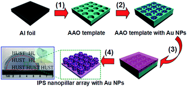
We report a facile and efficient way to fabricate a highly flexible, transparent and efficient surface-enhanced Raman scattering (SERS) substrate, in which Au nanoparticles (NPs) were embedded into the polymeric nanopillars via a nanoimprint lithography (NIL) method and using an anodic aluminum oxide (AAO) template. The obtained substrate exhibits prominent reproducibility and high sensitivity to Rhodamine 6G (R6G). Moreover, it possesses excellent transparency and flexibility. The SERS intensity acquired from these substrates almost remains constant after 200 bending cycles. Compared with traditional SERS substrates, this substrate represents a novel format with unique advantages, such as being highly flexible, transparent, lightweight, portable and easy to handle. More importantly, it can be scaled up for high-throughput production with low cost.


Introduction

SERS has been widely applied as a powerful tool for analytical chemistry, electrochemistry, catalysis and medical diagnostics, and can provide non-destructive and ultra-sensitive characterization down to single molecular level.1–3 To date, the attractive SERS characteristic triggered a gold rush for assembling noble metal nanostructures in order to utilize surface-plasmon-derived electric-field enhancements for the amplification of Raman scattering signals.4–9 However, the facile, cost-effective, and reproducible fabrication of SERS substrates on a large scale, while maintaining ultrahigh sensitivities, still remains challenging.10

For this purpose, various micro- and nano-fabrication techniques have been applied to fabricate periodic nanostructures, for instance, electron beam lithography, reactive ion etching, laser induced ablation, and focused ion-beam lithography.11–14 However, these techniques may not be commercially feasible due to a series of drawbacks such as complicated processing and high fabrication costs. NIL, by which the 3D topography of a mold can be duplicated onto polymeric resist materials in a simple stamping process, offers the possibility for the mass production of structures with high resolution at a low cost.15–17 Polymers possess a large number of advantages as host materials as they are cheap, stable, flexible, bio-compatible and can easily be processed.18 Besides, polymeric materials are highly transmissive in the visible and infra-red range, therefore reducing absorption processes. Furthermore, polymeric nanostructures can be easily integrated with other structures, such as mirrors or lenses, for even further improvement of the Raman excitation and scattered light collection.19

A transparent SERS-active substrate is a requisite for real-time and in situ Raman detection of chemical and biological targets. Recently, Wang et al.20 have reported the fabrication of a transparent SERS substrate made of Ag NPs on anodic aluminum oxide templates. This substrate can be used well in microbiological monitoring and in situ water pollutant detection. Flexible SERS substrates offer advantages over traditional rigid substrates in their flexibility to sense with non-planar geometries in terms of flexible or wearable labels. Moreover, they possess excellent mechanical strain resistance and can be easily tailored into any desired shape or size.21 For some applications such as packaging or tracking, flexible SERS substrates would be more appropriate.22 Therefore, the substrate with both excellent transparency and flexibility, while keeping high sensitivities, may be a prospective research direction in Raman spectroscopy. It is of great significance to bring SERS technology from the laboratory to real-world applications.

In the light of the above-mentioned needs for transparent and flexible SERS substrates, we report the fabrication of a flexible, transparent and sensitive substrate for SERS. Due to the easy fabrication, low cost and highly ordered nanostructure, AAO has been widely used as a template to prepare various nano-structured metals, metal oxides, polymers, and semiconductors. Here, as the initial mold, AAO combined with NIL, realized the transfer of a three-dimensional Au nanoparticle array to polymer film. The obtained substrate exhibits excellent sensitivity, reproducibility, transparency and flexibility. Moreover, it can be scaled up for high-throughput production with low cost. All of these factors imply that it is a perfect choice for practical application in SERS detection, especially for in situ detection.

Experimental

Materials and synthesis of AAO template

The porous AAO template was fabricated through a well-known two-step anodization process. In brief, organic cleaning and electropolishing were taken to the aluminum foil (99.999% in purity) prior to the anodization process. Under a temperature of 10 °C and voltage of 15 V, electropolishing was performed in a mixture consisting of 1/4HClO4 and 3/4C2H5OH for 5 min. The first anodization was carried out in 0.3 M (COOH)2 solution for 4 hours at a temperature of 3 °C and voltage of 40 V. Then, the oxide layer was dissolved in a mixture of 6 wt% H3PO4 and 1.8 wt% H2CrO4 at 60 °C. The second anodization lasted for 2 min under identical anodizing conditions, in order to obtain alumina pores with a low aspect ratio (depth/diameter) and free-standing polymer nanopillars. Subsequently, the pore-widening process was carried out for 150 s in 5 wt% H3PO4 solution at 60 °C. After that, the AAO was thoroughly rinsed with DI water and dried in air.

Fabrication of polymer nanopillar array with Au NPs

The deposition of Au NPs was carried out in a Kejing GSL-1100X-SPC16C sputtering evaporator with a sputtering current of 3 mA for 75 s. Subsequently, the IPS (a thermoplastic polyolefin film, developed by Obducat AB) was placed against the Au-decorated AAO template in an Eitre3 Nano Imprinter. NIL was performed at a temperature of 155 °C and a pressure of 40 bar for 20 min. After mechanically demolding, the substrate was obtained.

Characterization of the sample

The morphologies of the as-prepared samples were characterized by a Nova NanoSEM 450 scanning electron microscope (SEM). The transmittance spectra were obtained from a PerkinElmer Lambda 35 UV-VIS spectrophotometer. For Raman scattering measurements, 50 μL R6G aqueous solutions of different concentrations were dripped onto the as-prepared substrates and then dried in the dark. Raman measurements were performed using a HR800-UV Horiba-Jobin Yvon spectrometer coupled with an Olympus metallographic microscope. An Ar+ laser (λ = 514 nm) with a power of 5 mW served as the excitation source. The spectra were collected using a 100× microscope objective (N.A. = 0.9). The integration time was 10 s for each spectrum. All the measurements were carried out at room temperature.

Results and discussion

Characteristics of the substrate

Scheme 1 shows the strategy for the fabrication of the SERS-active substrate. It includes four steps, that is, anodizing Al foil, sputtering Au, NIL and mechanical peeling. NIL technology is a versatile and effective method with the advantages of high throughput, sub-10 nm feature and low cost.23 In the NIL process, under the effect of gas pressure, the melted polymer can enter into the holes in the alumina, and the remaining space is filled with polymer. This means that the Au NPs can be immersed into the melted polymer. During mechanical peeling off, the Au NPs along with solidified polymer are released.
image file: c6ra06329b-s1.tif
Scheme 1 Schematic illustration of the fabrication of the SERS substrate.

Fig. 1a displays photographs of the as-obtained SERS substrate. The nanopatterned IPS is colorless and transparent, so the IPS/Au composite displays the color of the Au NP array. After mechanical peeling off, the blue color was wholly transferred from the AAO template to IPS, indicating that the Au NPs were well inlaid into the IPS via the NIL method. The light blue color distributes homogeneously over the entire region, implying that the Au NPs are uniformly distributed. The substrate exhibits extraordinary flexibility, as can be easily seen from the inset of Fig. 1a. Fig. 1b depicts the transmittance spectrum of the substrate. The product exhibits excellent transparency in the visual and infra-red range, which can also be evidenced from Fig. 1a. The transmittance spectrum displays a strong broad band with a minimum at about 590 nm, which is a characteristic plasmon resonance band of Au NPs. The broadness of the plasmon resonance band may be attributed to the size nonuniformity of the Au NPs.


image file: c6ra06329b-f1.tif
Fig. 1 (a) Digital photographs of the as-obtained flexible and transparent SERS substrate. (b) Transmittance spectrum of the substrate.

Fig. 2a–d show the SEM images of the AAO template after sputtering with Au. It can be observed that the diameter and depth of the nanohole is ∼90 nm and ∼100 nm, respectively. A representative cross-sectional SEM image shows that the porous structure of AAO holds some Au NPs (5–15 nm) on the lateral wall, while most of Au NPs are immobilized at the bottom of the holes and on the top of the wall (Fig. 2d). As shown in Fig. 2e and f, the nanopillar array with Au NP inlays was formed well after the NIL process. The diameter of the nanopillars is about 90 nm. It is demonstrated that three-dimensional Au nanoparticle array can be well and truly transferred onto the polymer film via the NIL method.


image file: c6ra06329b-f2.tif
Fig. 2 (a–c) Representative SEM images of the AAO template after sputtering with Au at different magnifications. (d) Cross-sectional SEM image of the AAO template after sputtering with Au. (e and f) Typical SEM images of the SERS substrate.

SERS performance of the substrate

The SERS performance of the as-prepared substrate was evaluated by using R6G as the probe molecule. Fig. 3a displays the SERS spectra obtained from different concentrations of R6G adsorbed on the substrate. Obviously, all spectra show no obvious differences except for the SERS signal intensity. The spectral intensity decreases with diluting the concentrations of R6G, and Raman peak of R6G still can be identified clearly even at a concentration as low as 10−12 M. Therefore, this SERS substrate shows a very promising and practical solution to the ultratrace detection of analytes. There are six dominant Raman peaks centered at 615, 777, 1189, 1366, 1513 and 1653 cm−1, which are consistent with the Raman signals of R6G molecules.10 The Raman bands at 615, 777 and 1189 cm−1 can be attributed to the C–C–C ring in-plane vibration mode, the C–H out-of-plane bend mode and the C–H in-plane bending mode of the R6G molecule, respectively. Meanwhile the band at 1366, 1513 and 1653 cm−1 should correspond to the in-plane C–C stretching modes of R6G.24,25 Additionally, the Raman spectrum of the bare substrate was measured. It exhibited weak Raman signals and could be neglected when compared with signals of R6G under our experimental conditions.
image file: c6ra06329b-f3.tif
Fig. 3 (a) SERS spectra obtained from different concentrations of R6G adsorbed on the substrate. (b) SERS spectra of R6G (10−6 M) collected from 8 randomly selected acquisition points.

The reproducibility of Raman signals from the SERS substrate is of great importance for its practical use. To test whether the as-obtained substrates are able to give reproducible SERS signals of the target molecules, we collected the SERS spectra of R6G molecules with a concentration of 10−6 M from 8 randomly selected acquisition points on the substrate. As shown in Fig. 3b, the SERS spectra show very similar intensities and shapes. Moreover, we calculated the relative standard deviation (RSD) values corresponding to the six major SERS peaks of R6G, as shown in Table 1. For our substrate, all of the RSD values are below 10%. Both of the above discussions demonstrate that the substrate possesses excellent reproducibility throughout the entire substrate surface.

Table 1 RSD value for the major peaks of the R6G SERS spectrum
Peak position (cm−1) 615 777 1189 1366 1513 1653
RSD value 9.04% 9.23% 9.76% 8.86% 9.93% 9.28%


In this study, the intensity of the peak at 1653 cm−1 was chosen to estimate the enhancement factor (EF) of our substrate through the method described in a previous report.26 Here, the EF is calculated to be about 8.2 × 10⁷. That may be lower than the EF previously observed for R6G molecules on other substrates. However, previous reports have shown that an enhancement factor in the order of 107 to 108 is sufficient for the detection of a single molecule.27–29

In our experiments, we choose pyridine as the other probe molecule to test the obtained substrate, as shown in Fig. 4. The normal Raman spectrum and SERS spectrum were collected from pyridine and a 0.1 mM pyridine solution treated SERS substrate, respectively. Two ring breathing modes are observed in both the normal Raman spectrum and SERS spectrum. The EF can reach an order of magnitude of 106 by using the method mentioned in a previous report.30 Thus, this novel substrate can efficiently enhance the Raman signal intensities of molecules adsorbed on it.


image file: c6ra06329b-f4.tif
Fig. 4 Typical normal Raman spectrum and SERS spectrum of pyridine.

Flexibility performance of the substrate

For the substrate to be an effective detector, the flexible substrate should retain superior SERS performance during mechanical deformation. To investigate the flexibility, we compare the SERS spectra of R6G (10−6 M) obtained from the substrates under different mechanical bending conditions, as shown in insets of Fig. 5a. It is obviously observed that the Raman intensities under different bending angles remain almost constant in comparison with those under normal conditions. In our Raman measurements, the laser spot illuminated on the samples is ∼1 μm. No matter how large the macroscopical bending angle is, the area illuminated by the laser is almost planar. Neither the distance of the adjacent nanopillars, nor the electric fields of the adjacent Au NPs are changed remarkably. So the Raman intensities under different bending angles remain almost constant. Fig. 5b shows the SERS spectra of R6G (10−6 M) obtained from the substrates after various bending cycles (as shown in inset of Fig. 5b). It is noted that, even for the spectrum acquired from the substrates after 200 cycles, neither a shift in the dominant Raman peaks nor a significant change in Raman intensity occurred. The above results demonstrate that the substrate possesses remarkable flexibility and stability.
image file: c6ra06329b-f5.tif
Fig. 5 (a) SERS spectra of R6G (10−6 M) obtained from the substrates bent with different curvatures. (b) SERS spectra of R6G (10−6 M) obtained from the substrates after various bending cycles.

The excellent transparency, flexibility, and sensitivity of this substrate could open up new significant possibilities for more practical applications. The substrate perhaps could be used for the real-time and in situ Raman detection of chemical and biological targets.1,31 It may be able to achieve rapid testing, without the time-consuming processes of sample preparation.3,20 In junction with a portable Raman spectrometer, this substrate could have tremendous scope as a rapid, simple-to-use, field-portable and cost-effective analyzer.

Conclusions

In summary, by using an AAO template and NIL technology, we successfully fabricated a highly flexible, transparent and efficient SERS-active substrate. The obtained substrate displays a high SERS sensitivity to R6G so that a concentration as low as 10−12 M can still be identified and the EF was calculated to be about 8.2 × 10⁷. The EF for pyridine can reach an order of magnitude of 106. It exhibits prominent reproducibility and RSD values corresponding to the six major SERS peaks of R6G were all below 10%. Moreover, the polymer based SERS substrate possesses excellent transparency and flexibility. The SERS intensity acquired from these substrates almost remains constant after 200 bending cycles. This novel substrate offers a number of significant benefits over more conventional SERS substrates in that they are highly flexible, transparent, lightweight, portable and easy to handle. Additionally, it can be scaled up for high-throughput production with low cost.

Acknowledgements

This work was supported by the National High-tech R&D Program (863 Program) of China (Grant No. 2015AA043302), the National Natural Science Foundation of China (Grant No. 61474048) and the Fundamental Research Funds for the Central Universities of China (Grant No. HUST2015049).

Notes and references

  1. J. F. Li, Y. F. Huang, Y. Ding, Z. L. Yang, S. B. Li, X. S. Zhou, F. R. Fan, W. Zhang, Z. Y. Zhou, D. Y. Wu, B. Ren, Z. L. Wang and Z. Q. Tian, Nature, 2010, 464, 392–395 CrossRef CAS PubMed.
  2. J. F. Li, X. D. Tian, S. B. Li, J. R. Anema, Z. L. Yang, Y. Ding, Y. F. Wu, Y. M. Zeng, Q. Z. Chen, B. Ren, Z. L. Wang and Z. Q. Tian, Nat. Protoc., 2013, 8, 52–65 CrossRef CAS PubMed.
  3. T.-Y. Liu, K.-T. Tsai, H.-H. Wang, Y. Chen, Y.-H. Chen, Y.-C. Chao, H.-H. Chang, C.-H. Lin, J.-K. Wang and Y.-L. Wang, Nat. Commun., 2011, 2, 538 CrossRef PubMed.
  4. S.-G. Park, H. Hwang and S.-M. Yang, J. Mater. Chem. C, 2013, 1, 426–431 RSC.
  5. S. Nie and S. R. Emory, Science, 1997, 275, 1102–1106 CrossRef CAS PubMed.
  6. P. Nagpal, N. C. Lindquist, S.-H. Oh and D. J. Norris, Science, 2009, 325, 594–597 CrossRef CAS PubMed.
  7. H.-H. Wang, C.-Y. Liu, S.-B. Wu, N.-W. Liu, C.-Y. Peng, T.-H. Chan, C.-F. Hsu, J.-K. Wang and Y.-L. Wang, Adv. Mater., 2006, 18, 491–495 CrossRef CAS.
  8. S. Zhang, W. Ni, X. Kou, M. H. Yeung, L. Sun, J. Wang and C. Yan, Adv. Funct. Mater., 2007, 17, 3258–3266 CrossRef CAS.
  9. H.-W. Ting, Y.-K. Lin, Y.-J. Wu, L.-J. Chou, C.-J. Tsai and L.-J. Chen, J. Mater. Chem. C, 2013, 1, 3593–3599 RSC.
  10. M. Zhang, A. Zhao, D. Li, H. Sun, D. Wang, H. Guo, Q. Gao, Z. Gan and W. Tao, Analyst, 2012, 137, 4584–4592 RSC.
  11. L. Gunnarsson, E. J. Bjerneld, H. Xu, S. Petronis, B. Kasemo and M. Käll, Appl. Phys. Lett., 2001, 78, 802–804 CrossRef CAS.
  12. C.-H. Hsu, H.-C. Lo, C.-F. Chen, C. T. Wu, J.-S. Hwang, D. Das, J. Tsai, L.-C. Chen and K.-H. Chen, Nano Lett., 2004, 4, 471–475 CrossRef CAS.
  13. Y.-F. Huang, S. Chattopadhyay, Y.-J. Jen, C.-Y. Peng, T.-A. Liu, Y.-K. Hsu, C.-L. Pan, H.-C. Lo, C.-H. Hsu, Y.-H. Chang, C.-S. Lee, K.-H. Chen and L.-C. Chen, Nat. Nanotechnol., 2007, 2, 770–774 CrossRef CAS PubMed.
  14. J. Li, D. Stein, C. McMullan, D. Branton, M. J. Aziz and J. A. Golovchenko, Nature, 2001, 412, 166–169 CrossRef CAS PubMed.
  15. S. J. Barcelo, A. Kim, W. Wu and Z. Li, ACS Nano, 2012, 6, 6446–6452 CrossRef CAS PubMed.
  16. F. S. Ou, M. Hu, I. Naumov, A. Kim, W. Wu, A. M. Bratkovsky, X. Li, R. S. Williams and Z. Li, Nano Lett., 2011, 11, 2538–2542 CrossRef CAS PubMed.
  17. S. Krishnamoorthy, S. Krishnan, P. Thoniyot and H. Y. Low, ACS Appl. Mater. Interfaces, 2011, 3, 1033–1040 CAS.
  18. T. Hasell, L. Lagonigro, A. C. Peacock, S. Yoda, P. D. Brown, P. J. A. Sazio and S. M. Howdle, Adv. Funct. Mater., 2008, 18, 1265–1271 CrossRef CAS.
  19. W. Wu, M. Hu, F. S. Ou, Z. Li and R. S. Williams, Nanotechnology, 2010, 21, 255502 CrossRef PubMed.
  20. H.-H. Wang, T.-Y. Cheng, P. Sharma, F.-Y. Chiang, S. W.-Y. Chiu, J.-K. Wang and Y.-L. Wang, Nanotechnology, 2011, 22, 385702 CrossRef PubMed.
  21. D. He, B. Hu, Q.-F. Yao, K. Wang and S.-H. Yu, ACS Nano, 2011, 3, 3993–4002 CrossRef PubMed.
  22. J. P. Singh, H. Y. Chu, J. Abell, R. A. Tripp and Y. Zhao, Nanoscale, 2012, 4, 3410–3414 RSC.
  23. T. Sun, Z. Xu, S. Wang, W. Zhao, X. Wu, S. Liu, W. Liu, J. Peng, Z. Wang, X. Zhang and J. He, J. Nanosci. Nanotechnol., 2013, 13, 1871–1875 CrossRef CAS PubMed.
  24. K. Sun, G. Meng, Q. Huang, X. Zhao, C. Zhu, Z. Huang, Y. Qian, X. Wang and X. Hu, J. Mater. Chem. C, 2013, 1, 5015–5022 RSC.
  25. Y.-C. Liu, K.-H. Yang and T.-C. Hsu, J. Phys. Chem. C, 2009, 113, 8162–8168 CAS.
  26. H. Tang, G. Meng, Q. Huang, Z. Zhang, Z. Huang and C. Zhu, Adv. Funct. Mater., 2012, 22, 218–224 CrossRef CAS.
  27. D.-K. Lim, K.-S. Jeon, H. M. Kim, J.-M. Nam and Y. D. Suh, Nat. Mater., 2010, 9, 60–67 CrossRef CAS PubMed.
  28. P. G. Etchegoin and E. C. Le Ru, Phys. Chem. Chem. Phys., 2008, 10, 6079–6089 RSC.
  29. E. C. Le Ru, E. Blakie, M. Meyer and P. G. Etchegoin, J. Phys. Chem. C, 2007, 111, 13794–13803 CAS.
  30. H. X. Shen, W. J. Zou, Z. L. Yang, Y. X. Yuan, M. M. Xu, J. L. Yao and R. A. Gu, J. Opt., 2015, 17, 114014 CrossRef.
  31. X. Qian, X.-H. Peng, D. O. Ansari, Q. Yin-Goen, G. Z. Chen, D. M. Shin, L. Yang, A. N. Young, M. D. Wang and S. Nie, Nat. Biotechnol., 2008, 26, 83–90 CrossRef CAS PubMed.

This journal is © The Royal Society of Chemistry 2016
Click here to see how this site uses Cookies. View our privacy policy here.