
Vacancy-induced spin polarization in graphene and B–N nanoribbon heterojunctions
Xiaohui Jiangab,
Changfeng Fangb,
Dongqing Zouc,
Wenkai Zhaoc,
Wen Liub,
Xiangmu Kong*a and
Desheng Liu*bc
aCollege of Physics and Engineering, Qufu Normal University, Qufu 273165, China. E-mail: kongxm@mail.qfnu.edu.cn
bDepartment of Physics, Jining University, Qufu 273155, People's Republic of China. E-mail: liuds@sdu.edu.cn
cSchool of Physics, State Key Laboratory of Crystal Materials, Shandong University, Jinan 250100, People's Republic of China
First published on 6th June 2016
Abstract
By using nonequilibrium Green's functions (NEGF) and density functional theory (DFT), we investigate the spin-separated electronic transport properties in heterojunctions constructed by zigzag graphene and boron nitride nanoribbons. The results show that the heterojunctions exhibit a strong spin polarization and ferromagnetic state when there is a vacant position in the boron nitride nanoribbons (BNNRs). The spin-filter effect can be significantly tuned and improved by the species of the nitrogen and boron vacancy and the location of the vacancy in the boron nitride nanoribbons with the spin-filter efficiency (SFE) up to nearly 100%. The spin negative differential resistance (SNDR) properties at low bias can also be found in the proposed molecular spin devices. Mechanisms for the results are suggested, and these findings open up new possibilities for developing nano-spintronic devices.
Introduction
Since the discovery of graphene1 and the fabrication of quasi-one-dimensional graphene nanoribbons (GNRs),2 the electronic properties of GNRs have been paid much attention.3–6 GNRs can be constructed by “cutting” the graphene and consequently producing edges. According to the edge characteristics, there are two types of GNRs: armchair-edged GNRs (AGNRs) and zigzag-edged GNRs (ZGNRs). Particularly, ZGNR is one of the most studied prototypical GNRs due to the presence of the electronic edge states.7 Recent studies have also investigated the magnetic properties of ZGNRs and the possibility to design spin-polarized conductors by controlling their conductance,8–10 which shows that ZGNRs are believed to be the promising materials for spintronic devices. Moreover, the study of ZGNR is also crucial in the field of spintronics due to its potential application, such as high electron mobility, gate tunability and long spin lifetimes.Generally, the transport properties of GNRs are sensitive to many factors, like generate defects in GNRs,11,12 external electric/magnetic field,13,14 edges modification,15,16 adsorption,17 and doping nitrogen or boron atoms in GNRs18 for instance. These impact elements provide plenty of techniques for tuning and enlarge the applications of GNRs to a great extent. Tang and co-workers have recently found that by applying an external transverse electric field, the ZGNRs with an extended line defect can exhibit a strong spin polarization and ferromagnetic state.11 ZGNRs in antiferromagnetic state are shown to be semiconductors, however, they can be tuned to be half-metallic by edge decoration or by hybrid Boron–Carbon–Nitrogen (BCN) nanoribbons.19,20 Half-metallic materials are ideal candidates for spintronic applications because they have one metallic spin channel and one semiconducting or insulating spin channel. Therefore, the most important way to make the half-metallic ZGNR is to break the symmetry of the two edge states, then the spin polarized transport can be realized. Among all the possibilities, impurity doping is one of the most efficient ways for tuning the properties of GNRs.
Hexagonal boron nitride (h-BN) sheets have honeycomb lattice structures, sharing the similar crystalline structure with graphene. However, BN sheets are semiconductors with a band gap of about 4.5 eV, which makes them a potentially suitable substrate material to open a band gap for graphene.21 Recently, many theoretical and experimental studies have been focused on the lateral heterostructures of GNRs and BNNRs or the monolayer graphene between boron nitride sheets,22–24 and the results show that the hybridized in-plane lateral heterostructures could provide us opportunities towards atomically thin integrated circuitry. With controlling the interface properly between graphene/BN, the band gap and spin-relevant properties could be realized. Practically, it is difficult to fabricate perfect (ZBNNR)m–(ZGNR)n heterojunctions without defects. However, there is few study to the best of our knowledge on the spin electronic transport properties of the hybridization of ZGNRs and ZBNNRs with B vacancy and N vacancy. All these questions are essential for mono-atomic layer electronics and need to be thoroughly studied.
In this article, we present a detailed computational study about the boron vacancy and nitrogen vacancy in the hybridized ZBNNRs–ZGNRs two-probe devices under the ferromagnetic states. Systematic first-principles calculations are used to investigate the spin-separated electronic transport properties of both devices, and the spin-dependent results show an obvious SNDR phenomena while the device with nitrogen vacancy. Also nearly 100% SFE can be obtained with both nitrogen and boron vacancy.
Models and computational methods
The models composed of (ZBNNR)m–(ZGNR)n heterojunctions are shown in Fig. 1. The two-probe device is divided into three parts, the left electrode, the scattering region and the right electrode. The left and right electrodes are made of semi-infinite ZGNRs and the scattering region is the heterojunctions of ZBNNRs and ZGNRs. The hybridized ZBNNRs–ZGNRs structure can be formed with different ratios of the number of ZBNNR and ZGNR units—denoted as (ZBNNR)m–(ZGNR)n—where m is the number of the ZBNNR unit cells in the channel region, n indicates the number of the ZGNR unit cells in the channel region (except for the shielding layer of the electrode), and m plus n equals 8 (the length of the channel region). Our calculations have been performed by applying the non-equilibrium Green's functions combined with the density functional theory as implemented in Atomistix ToolKit.25 Double-zeta polarized basis sets are used as the local atomic numerical orbitals. The exchange correlation functional is described by the Perdew–Burke–Ernzerhof parameter of the spin generalized gradient approximations (SGGA.PBE), and the cutoff energy is set to 150 Ry. A 1 × 1 × 100 Monkhorst sampling in the Brillouin zone is utilized. These heterojunctions are modeled over 10 Å of vacuum space between neighboring cells to avoid interactions between periodic images. Before calculating the electronic transport properties, the convergence criteria of energy and all atoms in the channel region are relaxed with a force set to be 1 × 10⁻⁵ eV and 0.05 eV Å−1, respectively. The spin-dependent current through the scattering region can be calculated by Landauer–Büttiker formula26here, the σ = ↑ (up spin) and σ = ↓ (down spin), Tσ(E,Vb) is the bias and spin dependent transmission coefficient, and the energy region between

 and
and  is referred to as the bias window, which contributes to the current integral above. SFE is defined as
where T↑(Ef) and T↓(Ef) represent the transmission coefficient of the up and down spin channel at the Fermi level, respectively. At finite bias, the SFE is defined as
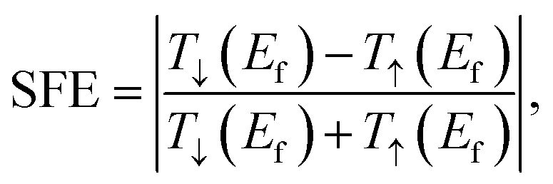
where I↑(Vb) and I↓(Vb) respectively represent the magnitude of the up and down spin current at finite bias.

 | ||
| Fig. 1 Schematics of (ZBNNR)m–(ZGNR)n two-probe device with nitrogen and boron vacancy. This system consists of the semi-infinite left electrode, the central scattering region, and the semi-infinite right electrode. m and n indicate the number of ZBNNR unit cells and ZGNR unit cells in the scattering region (except for the shielding layer of the electrode). B1, B2, B3, N1, N2, N3 represent the locations of the B and N vacancy, respectively. (a) Structure of (ZBNNR)4–(ZGNR)4 two-probe devices with boron or nitrogen vacancy; (b) structure of (ZBNNR)5–(ZGNR)3 two-probe devices with boron or nitrogen vacancy. | ||
Results and discussion
To investigate how these vacancies affect the electronic structures and to assess the magnitude of vacancy effect, Fig. 2 lists the equilibrium transmission spectra and the corresponding spin density distribution plots of (ZBNNR)4–(ZGNR)4 and (ZBNNR)5–(ZGNR)3 two-probe devices with nitrogen and boron vacancies located at different positions. From the graphs we can see all these transmission peaks appear within the transmission energy gap for all these defective devices compared with the original model.23 Moreover, it also can be seen that the species and the position of the vacancies have a profound effect on these transmission peaks, and the spin density distributions show that all these defect devices have strong edge effect and ferromagnetic coupled properties, and the magnitude of the spin density are strongly dependent on the species and the position of the vacancies. For (ZBNNR)4–(ZGNR)4 two-probe devices with nitrogen vacancy (Fig. 2a and b), and (ZBNNR)5–(ZGNR)3 two-probe devices with nitrogen vacancy (Fig. 2e–g), we can see distinct transmission spectra occur around Ef. While the nitrogen vacancy situated at the center of ZBNNRs (Fig. 2b, f and g), there are transmission peaks appear around the Ef, and the equilibrium spin polarized transmission spectra indicate a giant spin splitting, which are in accordance with the inset plots (the spin density distribution). At this situation, the spin density distribution on boron atoms at the vacancy are delocalized, and work as scattering centers for the propagating electronic wave functions along the nanoribbon, so the electrons flow through the heterojunction around the Ef and nearly 100% spin-filter efficiency can be obtained. Otherwise, while the nitrogen vacancy located at the ZBNNRs and ZGNRs' boundary (Fig. 2a and e), nearly no transmission peak appears among the transmission energy gap. The spin density distribution in boron atoms are localized, which is also reflected by the transmission spectra. Compared Fig. 2f with 2g, while the nitrogen vacancy situated near the nanoribbon's lower edge, the up spin channel is the main contribution to the conduction (Fig. 2f), otherwise, while the nitrogen vacancy situated near the nanoribbon's upper edge, the down spin channel is the main contribution to the conduction (Fig. 2g). For (ZBNNR)4–(ZGNR)4 two probe device with boron vacancy (Fig. 2c and d), and (ZBNNR)5–(ZGNR)3 two probe device with boron vacancy (Fig. 2h–j), in comparison with the nitrogen vacancy's transmission spectra, boron vacancy, however, can result in spin polarized transmission peaks within the transmission energy gap below the Ef, and the magnitude of the spin polarized peaks are larger when the vacancy situated at the center of ZBNNRs than the situation at the ZBNNRs and ZGNRs' boundary. From the point view of logic applications, the (ZBNNR)4–(ZGNR)4 and (ZBNNR)5–(ZGNR)3 two-probe devices with boron vacancy seem to be better than the devices with a nitrogen vacancy, based on the fact that the former ones would be much easier to be turned off than the latter ones. It is noticeable from the transmission that the nitrogen and boron vacancies can lead to spin polarization, and the magnitude of the polarization is much larger when the nitrogen or boron vacancy situated at the center of ZBNNRs, which suggesting that these devices can be used as a spin filter, so we choose (ZBNNR)5–(ZGNR)3–N2V, (ZBNNR)5–(ZGNR)3–N3V, (ZBNNR)5–(ZGNR)3–B2V, and (ZBNNR)5–(ZGNR)3–B3V two-probe device as the examples to investigate the spin polarized transport properties, and the spin-dependent I–V curves and SFE phenomena, as shown in Fig. 3. | ||
| Fig. 2 Equilibrium transmission spectra and corresponding spin density distributions of (ZBNNR)4–(ZGNR)4 and (ZBNNR)5–(ZGNR)3 two-probe devices with nitrogen and boron vacancy at different sites. The inset is ρ↑–ρ↓ for an iso-surface of ±0.008 e per Bohr3. The purple (blue) surface is for positive (negative) values. (a) (ZBNNR)4–(ZGNR)4–N1V device with nitrogen vacancy at site 1; (b) (ZBNNR)4–(ZGNR)4–N2V two-probe device with nitrogen vacancy at site 2; (c) (ZBNNR)4–(ZGNR)4–B1V two-probe device with boron vacancy at site 1; (d) (ZBNNR)4–(ZGNR)4–B2V two-probe device with boron vacancy at site 2; (e) (ZBNNR)5–(ZGNR)3–N1V two-probe device with nitrogen vacancy at site 1; (f) (ZBNNR)5–(ZGNR)3–N2V two-probe device with nitrogen vacancy site 2; (g) (ZBNNR)5–(ZGNR)3–N3V two-probe device with nitrogen vacancy at site 3; (h) (ZBNNR)5–(ZGNR)3–B1V two-probe device with boron vacancy at site 1; (i) (ZBNNR)5–(ZGNR)3–B2V two-probe device with boron vacancy at site 2; (j) (ZBNNR)5–(ZGNR)3–B3V two-probe device with boron vacancy at site 3. | ||
 | ||
| Fig. 3 The I–V and the corresponding SFE curves of (ZBNNR)5–(ZGNR)3 two-probe devices with nitrogen and boron vacancy at different sites. (a) (ZBNNR)5–(ZGNR)3–N2V two-probe device with nitrogen vacancy at site 2; (b) (ZBNNR)5–(ZGNR)3–N3V two-probe device with nitrogen vacancy at site 3; (c) (ZBNNR)5–(ZGNR)3–B2V two-probe device with boron vacancy at site 2; (d) (ZBNNR)5–(ZGNR)3–B3V two-probe device with boron vacancy at site 3; (k1) SFE in (ZBNNR)5–(ZGNR)3–N2V; (k2) SFE in (ZBNNR)5–(ZGNR)3–N3V; (k3) SFE in (ZBNNR)5–(ZGNR)3–B2V; (k4) SFE in (ZBNNR)5–(ZGNR)3–B3V. | ||
The I–V and the corresponding SFE curves of (ZBNNR)5–(ZGNR)3 two-probe devices with nitrogen and boron vacancy at different sites are shown in Fig. 3a–d. The SNDR phenomenon can be obviously observed in the device (ZBNNR)5–(ZGNR)3 with nitrogen vacancy (Fig. 3a and b), while in the situation of boron vacancy, the SNDR phenomenon is negligible (Fig. 3c and d). Therefore, the species of the vacancy are important for the SNDR behavior. For (ZBNNR)5–(ZGNR)3–N2V device, only the up spin channel behaves NDR, and starts at different biases, i.e., at −0.8 V and −0.5 V in the negative bias range, and at 0.7 V in the positive bias range. For the down spin channel nearly no NDR phenomenon occurs, and the currents holds small values. In the bias range of 0.0 V to 0.7 V, as shown by the polarization plot, the magnitude of the current in the up spin channel is significant larger than that in the down spin channel. For (ZBNNR)5–(ZGNR)3–N3V device, the NDR behavior occurs in both up spin and down spin channels. The down spin channel behaves an obvious NDR phenomenon at different biases in negative and positive bias ranges—in the negative bias starts at −0.5 V, and in the positive bias starts at 0.2 V—but the up spin channel only shows a small NDR phenomenon at 0.3 V. The magnitude of the current in the down spin channel is significant larger than that in the up spin channel in the bias range of −1.0 V to 0.2 V, which is also reflected by the polarization plot. For (ZBNNR)5–(ZGNR)3–B2V device and (ZBNNR)5–(ZGNR)3–B3V device, there are both differences and similarities in the up spin and down spin currents comparing with the N vacancy devices. The differences are containing two aspects, firstly, the magnitude of the currents with boron vacancy is much smaller than the currents with nitrogen vacancy; secondly, no obvious NDR phenomenon occurs during the bias range. The similarity is both of them having nearly 100% SFE. The insets (k1) and (k2) show that (ZBNNR)5–(ZGNR)3–N2V and (ZBNNR)5–(ZGNR)3–N3V two probe devices with nitrogen vacancy nearly have 100% SFE in the bias range of −0.2 V to 0.6 V and −0.8 V to 0.1 V, while (k3) and (k4) show (ZBNNR)5–(ZGNR)3–B2V and (ZBNNR)5–(ZGNR)3–B3V two probe devices with boron vacancy have 72% SFE at 0.2 V and 97% SFE in the bias range −0.2 V to 0.1 V, which means the SFE is sensitive to the species of vacancy and the positions of vacancy. As a result, it can be predicted that by controlling the vacancy effect, our designed devices do have promising applications in the future nanoelectronics.
To understand the SFE behavior, we choose the (ZBNNR)5–(ZGNR)3–N3V two probe device with nitrogen vacancy as the example. In Fig. 4a and b, we give transmission spectra and molecular energy levels in the scattering region at bias 0.1 V and 0.6 V, respectively. Besides, we also plot the molecular projected self-consistent Hamiltonian (MPSH) of the HOMO (the highest occupied molecular orbital) and LUMO (the lowest unoccupied molecular orbital) of the up spin and down pin channels, respectively. It is known from Landauer–Büttiker formula that the current is determined by the integral area of the transmission curve in the bias window. In Fig. 4a, it can be found that for down spin channel, there is one molecular orbital appearing in the bias window at 0.1 V (between the purple solid lines), and spatial distributions of the MPSH show that the HOMO and LUMO are delocalized. This means the electronic transport channels for down spin are open and large transmission can be expected. In contrast, for up spin channel, there is no molecular orbital appearing inside the bias window, and spatial distributions of the MPSH show that the HOMO and LUMO are all localized, thus the transmission is considerably weak, and the SFE phenomenon occurs. In Fig. 4b, it is clear that for the down spin channel, HOMO and LUMO orbitals are all in the bias window at 0.6 V, otherwise, for the up spin channel, only HOMO orbital in the bias window at 0.6 V, thus the electronic transmission capability for up spin channel is weaker than the down spin channel even though the LUMO for the up spin channel is delocalized. However, in comparison with Fig. 4a, the electronic transmission capability for up spin channel increases to a certain extent, resulting in a reduction in SFE, as shown in Fig. 3b. When there is no vacancy in (ZBNNR)5–(ZGNR)3 and (ZBNNR)4–(ZGNR)4 two probe devices, the up spin and down spin electrons are mainly transported by the opposite edge atoms.19 When introducing a vacancy on one side, the balance will be interrupted. Electronic states of one edge will be localized and the electronic states of the other edge are still delocalized. As a result, on the side with vacancy, the electronic transport ability is suppressed and on the other edge side it is almost not influenced. As a result, the spin polarized phenomenon occurs.
 | ||
| Fig. 4 Spin-separated transmission spectrum of (ZBNNR)5–(ZGNR)3–N3V two probe device with nitrogen vacancy at 0.1 V (a) and 0.6 V (b), respectively. The vertical purple solid lines stand for bias window, and the dash lines correspond to the spin-dependent frontier molecular orbitals. The insets of each figure give the MPSH of HOMO and LUMO under bias of 0.1 V and 0.6 V, respectively. | ||
For the SNDR phenomenon, the NDR behavior in the up spin channel of the (ZBNNR)5–(ZGNR)3–N2V two probe device in Fig. 3a is discussed as a prototype in this work. In Fig. 5, we show the transmission spectrum and the total density of states (TDOS) in the up spin channel of (ZBNNR)5–(ZGNR)3–N2V two probe device at 0.7 V, 0.8 V and 0.9 V, respectively. It is known that the current is determined by T(E,V) in the bias window. It is clearly seen from Fig. 5a that two portions of transmission peaks are in the bias window, and HOMO-2, HOMO-1, and HOMO orbitals are located in the bias window and make great contributions to the transmission, then leading to a large current at bias 0.7 V. As the bias increases from 0.7 V to 0.8 V, the bias window expands, but the integral areas decrease. In Fig. 5b, we can find HOMO-2, HOMO-1, and HOMO orbitals are located in the bias window, but they don't do any contributions to the transmission. As the bias increases to 0.9 V, more integral areas come into the bias window, and also HOMO-2, HOMO-1, and HOMO orbitals are located in the bias window. In order to understand this phenomenon, we plot the molecular projected self-consistent Hamiltonian (MPSH) of the HOMO orbital at 0.7 V, 0.8 V and 0.9 V, respectively. As we all know, the main contribution to the transport comes from the frontier molecular orbitals near the Fermi level. At bias 0.7 V, we can find HOMO orbital is fully delocalized through the whole scattering region. This means the electronic transport channels are open and large transmission can be expected. As the bias increases to 0.8 V, we can find the HOMO orbital is localized on the right part of the molecule. Note that when the orbital is delocalized through the whole molecule, an electron enters into the molecule at the energy of the orbital has a high probability of going through the molecule. So we can know that the frontier orbital is open for electronic transport at 0.7 V, while is suppressed at the bias 0.8 V, then the currents decrease deeply and the NDR phenomenon occurs during the bias. When the bias keeps on increasing to 0.9 V, from the inset of Fig. 5b, we can see at −0.18 eV, the electron states are localized on the right side of the molecule. Otherwise, from the inset of Fig. 5c, at −0.14 eV, the electron states are delocalized through the scattering region, improving the probability for electrons to transmit through the scattering region and thus leading to a small increase in the current at 0.9 V.
 | ||
| Fig. 5 The transmission spectrum and the total density of states (TDOS) of (ZBNNR)5–(ZGNR)3–N2V two probe device at 0.7 V (a), 0.8 V (b) and 0.9 V (c), respectively. The inset in (b): the corresponding local density of states (LDOS) at −0.18 eV. The inset in (c): the corresponding local density of states (LDOS) at −0.14 eV. The black line represents the transmission spectrum and the red line represents the total density of states. The region between the straight lines (purple color) is the bias window, three frontier molecular orbitals (black dashed-dotted lines) in the bias window. | ||
Conclusions
In conclusions, through first-principle quantum transport calculations, we have shown the spin polarized properties of vacancy-induced of zigzag graphene and boron nitride nanoribbons' heterojunctions. The electron transport properties of these devices show a great dependence on the species of the vacancy and the positions of the vacancy. Nearly perfect SFE and SNDR can be observed in our devices. While the nitrogen vacancy situates near the nanoribbon's lower edge, the up spin channel is the main contribution to the conduction. Otherwise, while the nitrogen vacancy situates near the nanoribbon's upper edge, the down spin channel is the main contribution to the conduction. The magnitude of the currents with boron vacancy is much smaller than the currents with nitrogen vacancy, and the currents are getting larger with the boron vacancy moving from the boundary's to the center. From which we can see the species of the vacancy and the position of the vacancy are the main factor to the conductance, and it indicates our devices have promising application in future nanoelectronics.Acknowledgements
This work was supported by the National Natural Science Foundation of China (Grant No. 11275112, 11574118 and 11404188).References
- K. S. Novoselov, A. K. Geim, S. V. Morozov, D. Jiang, Y. Zhang, S. V. Dubonos, I. V. Grigorieva and A. A. Firsov, Science, 2004, 306, 666 CrossRef CAS PubMed.
- M. Y. Han, B. Özyilmaz, Y. B. Zhang and P. Kim, Phys. Rev. Lett., 2007, 98, 206805 CrossRef PubMed.
- K. S. Novoselov, A. K. Geim, S. V. Morozov, D. Jiang and M. I. Katsnelson, Nature, 2005, 438, 197 CrossRef CAS PubMed.
- C. R. Dean, A. F. Young, I. Meric, C. Lee and L. Wang, Nat. Nanotechnol., 2010, 5, 722 CrossRef CAS PubMed.
- Y. Q. Wu, Y. M. Lin, A. A. Bol, K. A. Jenkins and F. Xia, Nature, 2011, 472, 74 CrossRef CAS PubMed.
- L. Lei, Y. C. Lin, M. Q. Bao, R. Cheng, J. W. Bai and Y. Liu, Nature, 2010, 467, 305 CrossRef PubMed.
- Y. Kobayashi, K. I. Fukui, T. Enoki and K. Kusakabe, Phys. Rev. B: Condens. Matter Mater. Phys., 2006, 73, 125415 CrossRef.
- O. V. Yazyev, Rep. Prog. Phys., 2010, 73, 56501 CrossRef.
- O. V. Yazyev and M. I. Katsnelson, Phys. Rev. Lett., 2008, 100, 47209 CrossRef PubMed.
- G. Cantele, Y. S. Lee, D. Ninno and N. Marzari, Nano Lett., 2009, 9, 3425 CrossRef CAS PubMed.
- G. P. Tang, J. C. Zhou, Z. H. Zhang, X. Q. Deng and Z. Q. Fan, Carbon, 2013, 60, 94 CrossRef CAS.
- B. An, S. Fukuyama, K. Yokogawa, M. Yoshimura, M. Egashira, Y. Korai and I. Mochida, Appl. Phys. Lett., 2001, 78, 3696 CrossRef CAS.
- E. Cruz-Silva, Z. M. Barnett, B. G. Sumpter and V. Meunier, Phys. Rev. B: Condens. Matter Mater. Phys., 2011, 83, 155445 CrossRef.
- Y. Y. Zhang, N. Jiang, S. X. Du, H. J. Gao, M. J. Beck and S. T. Pantelides, Nano Lett., 2010, 10, 1184 CrossRef PubMed.
- Y. W. Son, M. L. Cohen and S. G. Louie, Nature, 2006, 444, 347 CrossRef CAS PubMed.
- Y. Yoon and J. Guo, Appl. Phys. Lett., 2007, 91, 1984 Search PubMed.
- S. M. Choi and S. H. Jhi, Phys. Rev. Lett., 2009, 101, 266105 CrossRef PubMed.
- T. B. Martins, R. H. Miwa, A. J. R. D. Silva and A. Fazzio, Phys. Rev. Lett., 2007, 98, 196803 CrossRef CAS PubMed.
- E. J. Kan, Z. Y. Li, J. L. Yang and J. G. Hou, J. Am. Chem. Soc., 2008, 130, 4224 CrossRef CAS PubMed.
- D. Sudipta, A. K. Manna and S. K. Pati, Phys. Rev. Lett., 2009, 102, 096601 CrossRef PubMed.
- D. Usachov, V. K. Adamchuk, D. Haberer, A. Grüneis and H. Sachdev, Phys. Rev. B: Condens. Matter Mater. Phys., 2010, 82, 3484 CrossRef.
- A. Ramasubramaniam, D. Naveh and E. Towe, Nano Lett., 2010, 1, 1070 Search PubMed.
- J. C. Dong and H. Li, J. Phys. Chem. C, 2012, 116, 17259 CAS.
- J. Xu, S. K. Jang, J. Lee, Y. J. Song and S. Lee, J. Phys. Chem. C, 2014, 118, 22268 CAS.
- M. Brandbyge, J.-L. Mozos, P. Ordejón, J. Taylor and K. Stokbro, Phys. Rev. B: Condens. Matter Mater. Phys., 2002, 65, 165401 CrossRef.
- M. Büttiker, Y. Imry, R. Landauer and S. Pinhas, Phys. Rev. B: Condens. Matter Mater. Phys., 1985, 31, 6207 CrossRef.
| This journal is © The Royal Society of Chemistry 2016 |