
Large scale and cost effective generation of 3D self-supporting oxide nanowire architectures by a top-down and bottom-up combined approach†
Peixun Fan*ab,
Minlin Zhong*a,
Benfeng Baib,
Guofan Jinb and
Hongjun Zhanga
aLaser Materials Processing Research Centre, School of Materials Science and Engineering, Tsinghua University, Beijing 100084, PR China. E-mail: fpx@tsinghua.edu.cn; zhml@tsinghua.edu.cn
bState Key Laboratory of Precision Measurement Technology and Instruments, Department of Precision Instrument, Tsinghua University, Beijing 100084, PR China
First published on 4th May 2016
Abstract
Metal oxide nanowires are one of the most promising material systems utilized in energy conversion and storage devices. Directly synthesizing oxide nanowires on conductive substrates and assembling them into 3D self-supporting spatial architectures are of great importance for improving their performances. We propose and experimentally demonstrate a top-down and bottom-up combined manufacturing strategy, which can facilely fabricate various 3D self-supporting macro–micronano-nanowire multiscale architectures directly on bulk metal substrates. By employing micro–nano precursor structures, the gap between the commonly micrometer scale top-down and nanometer scale bottom-up approaches is bridged seamlessly. The presented strategy combines the advantages of the ultrafast laser direct writing approach in creating versatile micro patterns with those of the oxidation growth approach in creating elaborate nanowires. Both the precursor structures and the nanowires can be flexibly tuned in order to achieve arbitrary desired 3D architectures. Successfully pairing the scalable top-down laser direct writing technique with the high throughput bottom-up oxidation growth technique greatly improves the potential of our strategy in mass production and widespread adoption. Our approach opens a general and convenient route for integrating low dimensional oxide nanostructures with macroscopic metal substrates for various applications.
1. Introduction
In the development of nanoscience and technology over the past few decades, semiconductor metal oxide nanostructures have attracted significant research attention due to their potential applications in wide fields. Specifically, due to their tunable bandgaps, good electrical and optical characteristics, high catalytic activities and chemical stabilities, metal oxide nanowires have become one of the most promising material systems utilized in energy conversion and storage devices including photovoltaics,1,2 photodetectors,3 photoelectrochemical water splitting,4 lithium ion batteries,5 super capacitors,6 etc. Recently, as the requirements of the energy devices in high energy conversion efficiency, high power density as well as long cycle life keep being elevated, fabrication of controllable oxide nanowires and assembling them into complex multiscale structural hierarchies become increasingly important. As a typical representative, three dimensional (3D) extended nanowire structures directly constructed on conductive substrates, namely, the 3D self-supporting oxide nanowire architectures, possess advantages like high specific surface areas, fast active substance diffusions, accelerated electron/ion transportation, etc.7–14 And consequently, they have been an intensive focus of recent research on energy materials.Aiming to fulfill the above structure fabrication needs, various techniques via either the top-down or the bottom-up approaches have been attempted including etching,15 lithography,16,17 template-directed growth,18 physical/chemical deposition,19 solution synthesis,20 thermal oxidation,21 etc. Although these methods have been developed successfully and accordingly have given rise to great progress in different application fields, some critical researches are still needed to be conducted in order to better balance the requests in structure performance and manufacturing cost. Among that, the ability to synthesize oxide nanowires directly on their counterpart metal substrates and thus connect them with conventional macroscopic devices, the capability to form diverse and well-defined 3D multiscale architectures in a controllable fashion, the method for cost-effective and scalable growth of high-quality and uniformly aligned nanowires are under urgent demand for the practical applications in energy devices.
Inspired by the recent advances in nano fabrication techniques combining the top-down and bottom-up approaches,22–24 we present here an ultrafast laser hybrid manufacturing strategy to tackle the fundamental challenge in fabricating 3D oxide nanowire architectures directly self-supported on bulk metal substrates. The core idea of our strategy is to introduce micro–nano precursor structures by ultrafast laser via a top-down process, which serve as the seeds for the subsequent thermal oxidation growth of oxide nanowires via a bottom-up process. The nanowires grow on top of the micro–nano structures produced on bulk metal substrates, thus forming a self-supporting 3D macro–micronano-nanowire hierarchical system. The whole architectures are in situ constructed on the metal substrates with no additional materials needed. The presented strategy combines the advantages of the top-down ultrafast laser direct writing approach in creating versatile micro patterns with those of the bottom-up oxidation growth approach in creating elaborate nanowires. The ultrafast laser direct writing is a simple and scalable method with the ability to fabricate surface micro–nano structures over large area,25,26 while the thermal oxidation is a parallel growth method capable of high throughput synthesizing oxide nanowires.27–29 Therefore, successfully pairing these two techniques greatly improves the potential of our strategy in mass production and widespread adoption.
2. Experimental section
2.1. Fabrication of hierarchical structures
A Trumpf TruMicro 5000 laser system, which can generate 800 fs pulses at a central wavelength of 1030 nm, was utilized for the direct writing of micro–nano precursor structures. Before laser processing, the Cu (99.9% purity) and the Ti6Al4V samples with a dimension of 25 × 25 × 3 mm3 were mechanically polished to mirror finish and cleaned ultrasonically with ethanol to remove the oxide and grease on their surfaces. An x–y galvo was used to focus and scan the laser beam on the substrate surfaces in different patterns in atmospheric environment. The diameter of the focused spot, defined by an intensity drop to 1/e2 of the maximum value, was approximately 30 μm. Different types and patterns of surface micro–nano structures on the bulk metal substrates can be produced by controlling the laser processing parameters including the pulse energy, repetition rate, scanning speed, line spacing, etc. The specific laser processing parameters for fabricating micro–nano structures on different substrates can be found in Table S1 in the ESI.† Thermal oxidation of the bulk metal substrates with micro–nano structures were conducted in a horizontal-tube furnace, during which static air and an Ar/O2 mixed gas flow was employed for the growth of copper oxide nanowires (at 500 °C for 2 h) and titanium oxide nanowires (at 750 °C for 4 h), respectively.2.2. Characterization
The ultrafast laser directly written micro–nano structures as well as the thermal oxidation grown nanowires were observed with a scanning electron microscope (SEM, Oxford Instruments) incorporated with an energy-dispersive X-ray spectroscopy (EDS) accessory. An Olympus LEXT OLS4100 laser scanning confocal microscope was utilized for imaging and measuring the 3D microstructures and topographies of the sample surfaces. The XRD patterns were recorded by a Rigaku SmartLab X-ray diffractometer with a scanning speed of 4° min−1 in diffraction angle (2θ).3. Results and discussion
3.1. Method and mechanism for facilitated nanowire growth
As schematically illustrated in Fig. 1a, the entire process starts from surface patterning of bulk metal substrates by an ultrafast laser (Procedure 1). With such a procedure, versatile micro–nano structures can be directly written on metal surfaces (Structure 1), wherein, the ordered microscale structure arrays are mainly produced via a laser-inscribing process and the nanoscale as well as the disordered microscale structures are formed via a laser-inducing process.26,30,31 During laser inscribing, material ablation and removal occurs at the laser irradiated surface positions, leaving typically the periodic microscale patterns determined by laser machining routines. Instead, the laser-inducing is mainly a laser driving self-organization process, characterized by structures either with dimensions much smaller than the laser beam diameter or with spatial distributions which are obvious departures from the laser machining routines. Subsequently, the bulk metal samples with premade micro–nano structures are taken in a quartz boat and heated in a horizontal-tube furnace for thermal oxidation (Procedure 2). During this procedure, the premade micro–nano structures serve as the precursor on which self-supporting metal oxide nanowires are expected to grow. The bulk metal substrate, the ultrafast laser fabricated microscale and induced nanoscale features, together with the oxide nanowires, can construct a macro–micronano-nanowire multiscale hierarchical structure (Structure 2). | ||
| Fig. 1 (a) Schematic for the ultrafast laser hybrid manufacturing strategy (P1-Procedure 1, S1-Structure 1, P2-Procedure 2, S2-Structure 2). (b) and (c) SEM images of the nanowires grown in laser fabricated 1D periodic structures in low and high magnifications. (d) and (e) 3D laser confocal microscope images for the structures in (b) in grey and color charts, respectively. | ||
As a proof-of-concept, Fig. 1b–e shows the nanowires in situ synthesized via our approach on ultrafast laser directly written one dimensional (1D) periodic structures on Cu substrates. The nanowires grow perpendicularly to the lateral epidermis of the micro gratings and extend to the external space, reaching a length over 10 μm. EDS was employed for analyzing the element composition of the nanowires. Only two kinds of elements, i.e., Cu and O, were detected and the atomic percentage of both elements are approximately equal (Fig. S1†). Based on the location and intensity of the signal in the elemental mapping, the distribution of element O fits in well with that of Cu, and both elements spread uniformly along the entire skeleton of the nanowires. No obvious contrast between them was observed, which further confirms an equivalent content of both elements in the nanowires. Thus, the main phase constitution of the nanowires is identified to be cupric oxide. XRD characterizations also certified the new appearance of CuO phase on the sample surface after thermal oxidation (Fig. S2†). The relatively large scale Cu micro gratings serve as the transitional bridge connecting the oxide nanowires to the bulk metal substrates and play the role of skeleton to support the integrated surface architectures. The in situ grown oxide nanowires are tightly connected into the skeleton just like the grass taking root in the soil (Fig. S3†). The nanowires and the precursor structures are naturally combined, showing no obvious interface characteristics, making the constructed architectures a robust structural system.
Notably, in contrast to the developed growing state of nanowires at the lateral epidermis of the gratings, no nanowires have been observed at the top area of the gratings which is not directly irradiated by the laser pulses and thus has few precursor structures. This is in accordance with previous reports where it is not accessible or requires much longer periods (more hours or even days) to grow oxide nanowires on smooth Cu substrates with comparable thickness as in this work.27–29 Our results demonstrate that under the same thermal oxidation conditions, the existence of micro–nano precursor structures can facilitate and accelerate the oxide nanowire growth.
More importantly, when different kinds of precursor structures are introduced by ultrafast laser, the displayed facilitation effect to the nanowire growth will also be different. For illustrating this, two kinds of 1D periodic structures are intentionally fabricated through carefully controlling the ultrafast laser processing parameters, as shown in Fig. 2. Although the two grating structures seem similar from the microscale view, they are covered with different types of nanoscale features. The micro gratings in Fig. 2a are covered by nano ripple features (Fig. 2b), while those in Fig. 2e are covered with nano particle features (Fig. 2f). Massive papillae can be observed on the ripples which are finer and more homogeneous than the particle features in Fig. 2f. After thermal oxidation, oxide nanowires can grow on both kinds of micro–nano structures (Fig. 2c and g) but with distinguishing characteristics (Fig. 2d and h). In the former, thin and long nanowires in diameter of 50–80 nm align side by side compactly and cover the whole grating surfaces. Due to the small diameters accompanied with large length, some nanowires are bent at the wire top. Compared to that, the nanowires in the latter grow thicker to be 130–250 nm in diameter and less compact in distribution, but they are straighter and of higher stiffness. This effect can be positive for the controlled growth of oxide nanowires. Namely, if one would like to get slender and packed oxide nanowires, the ripple features decorated with fine papillae are preferred, whereas if one is more inclined to get straighter nanowires as well as more free space among them, the particle features are favoured. Considering that varied precursor structures can be intentionally produced by activating different laser–matter interaction mechanisms through adapting the process windows,30,31 the approach here provides a facile strategy to form nanowires with desired distribution.
 | ||
| Fig. 2 SEM images of nanowires grown on laser fabricated different kinds of 1D periodic structures: (a) and (b) 1D periodic microscale structures covered with nanoscale ripple features; (c) and (d) nanowires grown on the structures in (a) and (b); (e) and (f) 1D periodic microscale structures covered with nanoscale particle features; (g) and (h) nanowires grown on the structures in (e) and (f). | ||
To clarify how the precursors facilitate and accelerate the oxide nanowire growth, we made a schematic diagram analysis, as shown in Fig. 3. Currently, the mechanism underlying the formation of cupric oxide nanowires by thermal oxidation is still under debate. In spite of this, it is generally considered as a vapor–solid (VS) growth process29 where several critical factors are usually invoked to understand the observed phenomenon including the stress generation and release accompanying the interfacial reaction, the Cu atom transportation through the intermediates to the reaction interface, etc.32–35 As for the thermal oxidation on laser made micro–nano precursors, these factors can work as well. Beyond that, the precursors also play a seeding effect for the nanowire growth. It is reported that the rough positions at the oxide film where stress relaxes most would be the ideal sites for the nucleation of the CuO nanowires.33 Based on this, the surface rough grains actually perform the role of seeds or structure templates for the nanowire formation.34,35 More rough sites can render the Cu surface more seeds, alternately, more seeds imply more nucleus. As a result, more nanowires are expected to appear. Subsequently, as the Cu atoms diffuse to the nucleation sites, the nanowire nucleus grow up gradually via a stress-driven VS mechanism.
 | ||
| Fig. 3 Schematic showing the effect of surface micro–nano structures on the oxide nanowire growth: (a) smooth surface; (b) surface with ripple and fine papillae precursor structures; (c) surface with particle precursor structures. Different colors represent different compositions (orange-Cu, violet-CuO, blue-Cu2O). Red arrows indicate the Cu atom diffusion. | ||
For the smooth Cu substrates (Fig. 3a), few seeds exist on their surfaces. Besides, due to the intrinsic two-step reaction process from Cu to Cu2O then to CuO, the surface oxidation typically starts with the sequent growth of two parallel oxide layers, i.e., the bottom Cu2O layer and the top CuO layer.33–35 Thus, Cu surfaces will be fully covered by a dense film of Cu2O. The followed nanowire growth on top of the CuO layer requires the upward diffusion of Cu atoms across the compact Cu2O layer, which is difficult and relatively slow. Consequently, the CuO nanowire growth is confined and the area density as well as length of the nanowires are limited. When micro–nano precursors are introduced on Cu substrates (Fig. 3b and c), more seeds, namely more nucleation sites, are provided on the surfaces. At the same time, the situations for stress relaxation and Cu atom diffusion are improved. Abundant channels are supplied for the stress to relax and for the Cu atoms to transport upward to the reaction interface. Hence, both the nucleation and growing processes of the nanowires are enhanced, with their density and length being significantly increased. Also attributed to the seeding and structure template effect, the fine papillae on the nano ripple structures result in thin and correspondingly dense nanowires (Fig. 3b), while the relatively larger nano particles result in thicker nanowires. Meanwhile, due to the dimension variation of the nano particles, not all of them can be triggered synchronously as active sites for the nanowire growth. Only large oxide grains can be formed on the top of coarse particles. Thus, the nanowire distribution becomes less compact (Fig. 3c).
3.2. Large scale non-flaking growth of nanowires
The facilitation effect of precursor structures to the nanowire growth can be utilized for selectively synthesizing oxide nanowires on specific substrate areas. For demonstrating this, we conducted ultrafast laser direct writing on Cu substrates in the patterns of “TSINGHUA UNIVERSITY” fonts. As shown in Fig. 4, all the surface areas with premade micro–nano structures can yield substantial and well aligned oxide nanowires after thermal oxidation, where multiscale architectures are constructed. In contrast to that, the surface areas without premade structures seldom generate oxide nanowires. It is identified that oxide nanowires can preferentially grow on the ultrafast laser activated metal surface areas. The results further suggest that obviously distinct microcosmic reaction environments have been indeedly built at the surface zones with and without precursor structures, although the designated thermal oxidation conditions are completely the same. | ||
| Fig. 4 SEM images of nanowires grown on Cu surface partially treated by ultrafast laser: (a) and (b) areas untreated by laser; (c) and (d) areas treated by laser in the pattern of letter “H”; (e) and (f) areas treated by laser in the pattern of letter “A”. | ||
Through comparison of the macroscale photographs of oxidized Cu surfaces with different pre-treating conditions, the importance of the precursor structures can be appreciated more clearly (Fig. S4†). The oxide layer on the polished Cu surface exhibits obvious exfoliation and flaking, which becomes even more serious during the subsequent sample characterizations. Conversely, the Cu surface wholly treated by ultrafast laser is completely and evenly covered with oxide nanowires, showing exfoliation- and crack-free characteristics. On the Cu surface with ultrafast laser premade “TSINGHUA UNIVERSITY” patterns, only the pre-treated areas get well preserved after oxidation and severe exfoliation occurs on the other areas. These results evidence that the micro–nano precursors can provide a pinning and protecting effect for the nanowires and prevent the oxide scales from exfoliation. It is known that the flaking and cracking problems result from the thermal stress accumulation caused by the volume mismatch between the Cu substrate and the oxide layers.27,32 In the past, one conventional method to avoid cracking and exfoliation during thermal oxidation is to adopt Cu substrates with particular microscale dimensions, which allow the misfit stress to relax by deforming the thin substrates themselves.27,29 Nevertheless, it is still a great challenge to grow oxide nanowires on bulk Cu substrates without exfoliation. Other methods are also reported by selectively depositing films of growing32 or inhibiting27 sources on specified surface regions, which help in reducing the stress by permitting its release at the edges of the patterned deposits. Inspired by these studies, we utilize the laser beam to pattern the surfaces into microscale regions as precursor structures. In this condition, the stress accumulation occurs in relatively isolated small areas rather than on the whole sample surfaces, and thus the stress intensity is decreased. For another hand, the discontinuous and roughened surface renders the stress more freedom and channels to relax. As a result, the flaking and cracking problems can be settled eventually.
For further demonstrating this, we have prepared only sub-microscale structures on a Cu substrate by ultrafast laser as a contrast. Nanowires can still be achieved after thermal oxidation, however, the Cu surface became fragmented (Fig. S5†). It is indicated that although the sub-microscale structures have offered a certain interspace for the stress to relax, the stress accumulation issue still exists because the surface remains intact. Hence, the contribution of laser patterning to avoid cracking of the Cu substrates can be identified and the micro–nano dual-scale structures are indispensable for the non-flaking growth of oxide nanowires. In addition, another advantage of the laser patterning approach over the film depositing methods is that various micro–nano structures can be facilely formed which are beneficial for assembling the nanowires into desired 3D architectures as shown later. Our strategy can break the restraints in the substrate thickness for thermal oxidation approach and presents an adaptable solution for oxide nanowire growth on Cu substrates with arbitrary macroscale dimensions. Owing to this, the large area fabrication of oxide nanowires as well as the multiscale architectures can be guaranteed.
3.3. Controlled growth of oxide nanowires
Based on the knowledge of the distinct microcosmic reaction environments with and without precursor structures, we can intentionally change the dimensions of the laser premade structures and their spacing; then, via the subsequent thermal oxidation, the spatial distribution of nanowires can be directly adjusted. Take the fabrication of two dimensional (2D) periodic structures like micro cone arrays, for example (Fig. 5). Fig. 5g and h shows that remarkable 3D macro–micronano-nanowire hierarchical structures with the micro cone arrays as the skeleton have been successfully fabricated through our hybrid manufacturing strategy. From Fig. 5a–c and e, the periodicities of the micro cone arrays are gradually increased. Meanwhile, the central smooth areas on the top of cones which are not irradiated by the laser pulses get large. As a result, the surface areas covered by the nanowires are decreased (Fig. 5b, d and f). Given that the ultrafast laser direct writing is a program-controlled process, the density of the nanowires and their content on the metal surfaces also become programmable, which is crucially significant for the improvement of their physical and chemical properties. As an example, we have studied the impact of the distribution of the macro–micronano-nanowire hierarchical structures on their optical properties and achieved over 99% light absorption in the mid-infrared spectrum.36 Previously, the modifications of diameter, length and distribution density of oxide nanowires are mainly completed by carefully controlling the heating atmosphere, the heating temperature as well as the incubation time during thermal oxidation.29,32 The significance of our strategy lies in the fact that the modification of the nanowire morphologies is forward shifted to be accomplished by controlling the precursor structures, which is easy to implement by the ultrafast laser direct writing technique. As such, the large-scale parallel and controlled growth of nanowires can be realized concurrently. | ||
| Fig. 5 SEM images in low (a) (c) (e) and high (b) (d) (f) magnifications of nanowires grown on laser fabricated 2D periodic structures with different periodicities. (g) and (h) 3D confocal microscope images for structures in (a) in grey and color charts, respectively. | ||
3.4. 3D self-supporting nanowire architectures
Further, with the capability in driving the growth of oxide nanowires and the ability to seamlessly integrate them with larger scale metal structures and substrates, we demonstrate the fabrication of more complex 3D multiscale architectures, as shown in Fig. 6. 2D periodic structures in the shape of disordered spindles (Fig. 6a), fractal particle cluster structures (Fig. 6d), and vivid helical structures are separately written on Cu substrates by ultrafast laser. In spite of the strikingly different forms and shapes of those premade micro–nano structures, oxide nanowires have succeeded in growing out of their surfaces insusceptibly (Fig. 6b, e, g and h). The nanowires take root in the precursor structures and extend radially from their exteriors toward the free space, reaching a length from several to over 10 μm (Fig. 6c, f and i). Apparently, the precursor structures have offered a definitive guidance to the oxide nanowires on their spatial locations as well as a transitional bridge linking them with the macroscopic metal substrates. Owing to such effects, the establishment of 3D user-definable macro–micronano-nanowire multiscale architectures can be expected. The confocal microscope images for the corresponding hierarchical structures are presented in Fig. S6.† There have been several studies focusing on the patterned growth of oxide nanowires via thermal oxidation by selectively depositing the barrier27 or seed30 materials on set areas of the targeted substrates. The yielded nanowires are usually restricted to display only one fixed orientation, i.e., vertically up. Here in the present work, we not only avoid the complicated material deposition procedures, but also provide higher precision and more flexibility in controlling the nanowire growth patterns. More significantly, through guiding and configuring the nanowire growth along the topological precursor structures, the 3D distribution of the nanowires in arbitrary spatial orientations and their assembling to 3D structural systems can be fulfilled. | ||
| Fig. 6 SEM images of nanowires grown on laser fabricated different kinds of micro–nano structures: (a) 2D disordered structures; (b) and (c) nanowires grown on structures in (a); (d) particle cluster structures; (e) and (f) nanowires grown on structures in (d); (g)–(i) nanowires grown on helical structures. | ||
3.5. Applicability on varied metal substrates
Till now, all the results and discussions are based on copper. Yet, it should be noted that the ultrafast laser direct writing is a unique technique with no apparent material dependence; meanwhile, thermal oxidation has been proved effective in synthesis different kinds of metal oxide nanowires.37–42 In this regard, we anticipate the ultrafast laser hybrid manufacturing strategy to be also applicable in creating the 3D self-supporting multiscale architectures on other metal substrates. As illustrative instances, we implemented our strategy on substrates of titanium as well as its alloys. Fig. 7 shows a typical result we have achieved on Ti6Al4V surfaces. Encouragingly, abundant nanowires with diameters of 50–80 nm have been successfully grown on of the ultrafast laser premade structures, reaching a length of 5–10 μm. As can be seen, the microscale granular and columnar precursors are fully enwrapped by the densely and uniformly distributed nanowires, forming exquisite fluffy dandelion-like architectures.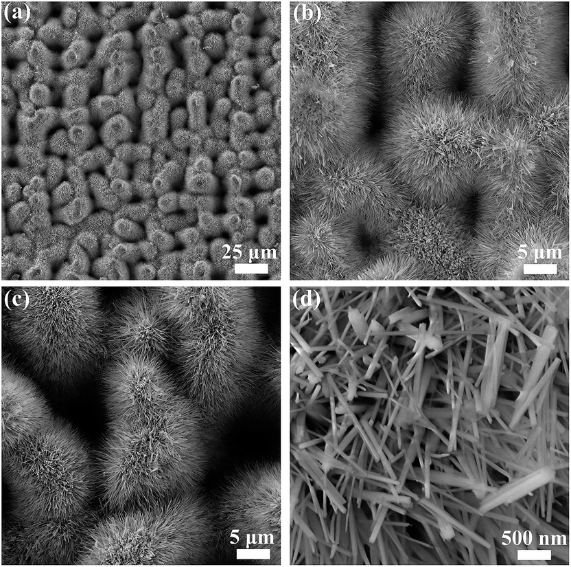 | ||
| Fig. 7 SEM images of nanowires grown on laser fabricated micro–nano structures on Ti6Al4V surface. | ||
EDS analysis in the nanowires only detected three kinds of elements, i.e., Ti, Al and O (Fig. S7†). The elemental mapping shows that the O atoms distribute uniformly along the skeleton of nanowires, indicating their primary chemical composition as oxides. Given that the atomic percentages cannot distinguish the specific oxide species and are susceptible to the interference of the substrates, we further conducted the XRD characterizations, and certified the new appearance of rutile TiO2 phase on the sample surface after thermal oxidation (Fig. S8†). Thus, a main phase constitution of titanium oxide is confirmed in the nanowires. Based on this, we speculate that the micro–nano precursor structure fabrication via ultrafast laser can be a general method for facilitating the synthesis of oxide nanowires, and bridging the gap between the 1D nanoscale structures and the bulk macroscale metal substrates. Additionally, we believe that the ultrafast laser written precursors is not constrained to be effective for the VS thermal oxidation process, but could also be of referential value for the other bottom-up synthesis approaches like hydrothermal, solvothermal, e.g. with this in mind, it can be promising to construct 3D multiscale architectures with nanowires of other kinds of metal oxide being integrated.
4. Conclusions
We propose and experimentally demonstrate an ultrafast laser hybrid nano manufacturing strategy which combines the advantages of top-down ultrafast laser direct writing approach and those of bottom-up thermal oxidation growth approach, with various 3D self-supporting macro–micronano-nanowire architectures being facilely produced on bulk metal substrates. Our strategy possesses advantages as follows: (1) growth of oxide nanowire is facilitated and accelerated via employing micro–nano precursor structures, making it a high throughput process; (2) exfoliation and flaking problems of the oxide scales are successfully avoided, making it accessible in large area fabrication; (3) dimensions and spatial distributions of nanowires can be flexibly modified by controlling the ultrafast laser written micro–nano precursors; (4) synthesized oxide nanowires are under protection of microscale skeletons which are supported by macroscale metal substrates, thus forming natural 3D multiscale architectures; (5) the combination of the microscale skeleton with the nanowires provides more tunable variances for achieving desired spatial hierarchies in specific application domains. No conventional nanofabrication techniques like lithography or deposition are required, making the presented process cost effective to be scaled up. Our strategy is applicable for in situ integrating varied oxide nanowires onto the corresponding metal substrates, making it promising to be a general and convenient routine in fabricating complex 3D hierarchical components for different functional devices.Acknowledgements
We acknowledge the support by the National Natural Science Foundation of China (Grant No. 51210009, 51575309, 11474180) and the National Key Basic Research and Development Program of China (Grant No. 2011CB013000).References
- T. J. Kempa, R. W. Day, S. Kim, H. Park and C. M. Lieber, Energy Environ. Sci., 2013, 6, 719–733 CAS.
- W. Wu, H. Feng, H. Rao, Y. Xu, D. Kuang and C. Su, Nat. Commun., 2014, 5, 3968 CAS.
- T. Zhai, L. Li, X. Wang, X. Fang, Y. Bando and D. Golberg, Adv. Funct. Mater., 2010, 20, 4233–4248 CrossRef CAS.
- F. Su, T. Wang, R. Lv, J. Zhang, P. Zhang, J. Lu and J. Gong, Nanoscale, 2013, 5, 9001–9009 RSC.
- L. Mai, Q. Wei, Q. An, X. Tian, Y. Zhao, X. Xu, L. Xu, L. Chang and Q. Zhang, Adv. Mater., 2013, 25, 2969–2973 CrossRef CAS PubMed.
- X. Lu, T. Zhai, X. Zhang, Y. Shen, L. Yuan, B. Hu, L. Gong, J. Chen, Y. Gao, J. Zhou, Y. Tong and Z. L. Wang, Adv. Mater., 2012, 24, 938–944 CrossRef CAS PubMed.
- Q. Zhang, E. Uchaker, S. L. Candelaria and G. Cao, Chem. Soc. Rev., 2013, 42, 3127–3171 RSC.
- Z. Zhou, N. Tian, J. Li, I. Broadwell and S. Sun, Chem. Soc. Rev., 2011, 40, 4167–4185 RSC.
- J. Jiang, Y. Li, J. Liu, X. Huang, C. Yuan and X. W. D. Lou, Adv. Mater., 2012, 24, 5166–5180 CrossRef CAS PubMed.
- T. Zhai, L. Li, Y. Ma, M. Liao, X. Wang, X. Fang, J. Yao, Y. Bando and D. Golberg, Chem. Soc. Rev., 2011, 40, 2986–3004 RSC.
- C. Cheng and H. J. Fan, Nano Today, 2012, 7, 327–343 CrossRef CAS.
- B. L. Ellis, P. Knauth and T. Djenizian, Adv. Mater., 2014, 26, 3368–3397 CrossRef CAS PubMed.
- R. K. Joshi and J. J. Schneider, Chem. Soc. Rev., 2012, 41, 5285–5312 RSC.
- J. Jiang, Y. Li, J. Liu and X. Huang, Nanoscale, 2011, 3, 45–58 RSC.
- Q. Hao, L. Chen and C. Xu, ACS Appl. Mater. Interfaces, 2014, 6, 10107–10112 CAS.
- D. P. Singh, A. George, R. V. Kumar, J. E. Ten Elshof and M. Wagemaker, J. Phys. Chem. C, 2013, 117, 19809–19815 CAS.
- C. Yue, Y. Yu, J. Yin, T. Wong, Y. Zang, J. Li and J. Kang, J. Mater. Chem. A, 2013, 1, 7896–7904 CAS.
- L. Taberna, S. Mitra, P. Poizot, P. Simon and J. M. Tarascon, Nat. Mater., 2006, 5, 567–573 CrossRef PubMed.
- R. S. Devan, R. A. Patil, J. Lin and Y. Ma, Adv. Funct. Mater., 2012, 22, 3326–3370 CrossRef CAS.
- X. Xia, Y. Zhang, D. Chao, C. Guan, Y. Zhang, L. Li, X. Ge, I. M. Bacho, J. Tu and H. J. Fan, Nanoscale, 2014, 6, 5008–5048 RSC.
- L. Liao, B. Yan, Y. F. Hao, G. Z. Xing, J. P. Liu, B. C. Zhao, Z. X. Shen, T. Wu, L. Wang, J. T. L. Thong, C. M. Li, W. Huang and T. Yu, Appl. Phys. Lett., 2009, 94, 113106 CrossRef.
- S. W. Chung, D. S. Ginger, M. W. Morales, Z. F. Zhang, V. Chandrasekhar, M. A. Ratner and C. A. Mirkin, Small, 2005, 1, 64–69 CrossRef CAS PubMed.
- M. Schaffner, G. England, M. Kolle, J. Aizenberg and N. Vogel, Small, 2015, 11, 4334–4340 CrossRef CAS PubMed.
- G. Zhang, C. Rainville, A. Salmon, M. Takiguchi, K. Tateno and H. Gotoh, ACS Nano, 2015, 9, 10580–10589 CrossRef CAS PubMed.
- Y. Zhang, Q. Chen, H. Xia and H. Sun, Nano Today, 2010, 5, 435–448 CrossRef CAS.
- L. Li, M. Hong, M. Schmidt, M. Zhong, A. Malshe, B. H. In'TVeld and V. Kovalenko, CIRP Annals-Manufacturing Technology, 2011, 60, 735–755 CrossRef.
- F. Mumm and P. Sikorski, Nanotechnology, 2011, 22, 105605 CrossRef CAS PubMed.
- Y. W. Zhu, T. Yu, F. C. Cheong, X. J. Xui, C. T. Lim, V. Tan, J. Thong and C. H. Sow, Nanotechnology, 2005, 16, 88–92 CrossRef CAS.
- X. C. Jiang, T. Herricks and Y. N. Xia, Nano Lett., 2002, 2, 1333–1338 CrossRef CAS.
- K. M. T. Ahmmed, C. Grambow and A. M. Kietzig, Micromachines, 2014, 5, 1219–1253 CrossRef.
- J. Cheng, C. S. Liu, S. Shang, D. Liu, W. Perrie, G. Dearden and K. Watkins, Opt. Laser Technol., 2013, 46, 88–102 CrossRef.
- K. Zhang, C. Rossi, C. Tenailleau, P. Alphonse and J. Chane-Ching, Nanotechnology, 2007, 18, 275607 CrossRef.
- R. Wang and C. Li, Cryst. Growth Des., 2009, 9, 2229–2234 CAS.
- L. Yuan and G. Zhou, J. Electrochem. Soc., 2012, 159, C205–C209 CrossRef CAS.
- L. Yuan, Y. Wang, R. Mema and G. Zhou, Acta Mater., 2011, 59, 2491–2500 CrossRef.
- P. Fan, B. Bai, J. Long, D. Jiang, G. Jin, H. Zhang and M. Zhong, Nano Lett., 2015, 15, 5988–5994 CrossRef CAS PubMed.
- M. M. Arafat, A. S. M. A. Haseeb, B. Dinan and S. A. Akbar, Ceram. Int., 2013, 39, 6517–6526 CrossRef CAS.
- M. M. Arafat, A. S. M. A. Haseeb and S. A. Akbar, Ceram. Int., 2015, 41, 4401–4409 CrossRef CAS.
- C. X. Zhao, Y. F. Li, J. Zhou, L. Y. Li, S. Z. Deng, N. S. Xu and J. Chen, Cryst. Growth Des., 2013, 13, 2897–2905 CAS.
- S. Park, S. An, H. Ko, C. Jin and C. Lee, ACS Appl. Mater. Interfaces, 2012, 4, 3650–3656 CAS.
- L. Yuan, R. Cai, J. I. Jang, W. Zhu, C. Wang, Y. Wang and G. Zhou, Nanoscale, 2013, 5, 7581–7588 RSC.
- F. Xu, A. Fahmi, Y. Zhao, Y. Xia and Y. Zhu, Nanoscale, 2012, 4, 7031–7037 RSC.
Footnote |
| † Electronic supplementary information (ESI) available: Specific laser processing parameters; composition detection of nanowires on Cu substrate; XRD patterns of Cu surfaces; highly magnified SEM images of nanowires; photographs of Cu surfaces after thermal oxidation; SEM images for oxidized Cu surface with only sub-microscale premade structures; 3D confocal microscope images of different architectures; composition detection of the nanowires on Ti6Al4V substrate; XRD patterns of Ti6Al4V surfaces. See DOI: 10.1039/c6ra06222a |
| This journal is © The Royal Society of Chemistry 2016 |