
Switchable diode effect in BaZrO3 thin films
Ying Dingab,
Xing Xub,
Amar Bhallac,
Xiubo Yanga,
Jianghua Chena and
Chonglin Chen*b
aCentre for High Resolution Electron Microscopy, College of Material Science and Engineering, Hunan University, Changsha 410082, China
bDepartment of Physics and Astronomy, University of Texas at San Antonio, San Antonio, TX 78249, USA. E-mail: cl.chen@utsa.edu
cDepartment of Electrical and Computer Engineering, University of Texas at San Antonio, San Antonio, TX 78249, USA
First published on 15th June 2016
Abstract
Resistive switching behaviour and switchable diode effects in BaZrO3 thin film were systematically studied to understand the charge trapping/detrapping behaviour for memory device applications. The switchable diode effect was studied by designing and fabricating a device in the multilayered structure of Ag/BaZrO3/SrRuO3. The as-grown BaZrO3 film shows bi-layered structure, in which the top layer is polycrystalline while the bottom layer grows epitaxially with the SrRuO3. The charge trapping/detrapping at the metal/insulator interface depletion layer was found to be the mechanism in governing the resistance switching effects. Besides, improved retention properties were achieved from the as-designed structures. Interface states caused by grain boundaries are assumed to be the reason. The findings of these diode characters may provide valuable information for the understanding of resistive switching in oxide materials.
Introduction
Traditional memories are approaching their physical limit as devices downscale in size.1 Candidates for equivalent scaling based on new materials have attracted a great attention for the next-generation of nonvolatile memories,2–6 wherein metal oxides resistance random access memory (ReRAM), a resistive switching (RS) device, features with high-speed switching, high-density data storage, and nondestructive readout.7–9The switchable diode effect is a typical resistive switching behaviour,10 in which the current–voltage (I–V) characteristics of the metal–insulator–metal (MIM) structure at a low applied electrical voltage has a rectifying behavior. The direction of the diode can be reversed by changing the polarity of the external bias.11 The rectifying conduction characteristics were initially investigated by Blom et al. in Au/PbTiO3/(La,Sr)CoO3 structure.12 Recent studies were mostly focused on the ferroelectric materials, especially in the BiFeO3 system.13 In the metal–ferroelectric–metal (MFM) structure, both polarization flipping and the electro-migration of chemical defects such as oxygen vacancies were found to be the key factors for the switching mechanisms but with an large applying voltage pulse.11 For the non-ferroelectrics, only SnO2 and Ba0.7Sr0.3TiO3 have been observed to show the switchable diode effect.14,15 The switchable diode effect in the SnO2 single nanowire device results from the Schottky barrier heights tuned by electro-migration of oxygen vacancies under the external applied bias of 2 MV m−1. Such a device shows excellent performance in endurance and retention time. While the mobility of oxygen vacancy in typical perovskite oxides at room temperature is very low, the resistive switching nature in Pt/Ba0.7Sr0.3TiO3/Pt planar device is mainly from the interface Schottky barrier modulation through charge trapping/detrapping at the Pt/Ba0.7Sr0.3TiO3 interface under the applied field of 15 MV m−1. However, such a device is suffered from low retention time probably due to the exposed oxygen vacancies can be easily compensated by surrounding electrons to restore the Schottky barrier.14
BaZrO3 (BZO) is a typical perovskite and characterized by good chemical stability. Compared with BaZrTiO3, BZO has simpler structure and properties.16 First, BZO shows uniform crystal structure without local polar clusters/regions. Second, BZO is a pure dielectric without dispersive nature and hysteresis effects. Therefore BZO is good candidate for the research on the effects of oxygen vacancies in the resistive switching. Recently, we have systematically investigated the switchable diode effect with improved data retention in the oxygen deficiency BZO thin films to understand the nature of the oxygen vacancy induced resistive switching behaviour. Our findings on the charge trapping/detrapping-induced band bending and the variation of the traps energy distribution at the interface Schottky contact indicate that the interface states caused by grain boundaries may play an important role in controlling the switchable diode effect.
Experimental
BaZrO3/SrRuO3 (BZO/SRO) multilayers on the (001) SrTiO3 (STO) single crystal substrates (see Fig. 1) were grown by the pulsed laser deposition (PLD) with the optimal growth condition.17–19 Briefly, the films were grown with a KrF excimer laser of 248 nm wavelength with an energy density of about 1.5 J cm−2 and a repetition rate of 4 Hz under 800 °C. In order to have oxygen vacancies in the BZO thin films, the oxygen pressure was maintained at 10 mTorr. The SRO bottom electrodes were deposited under the same condition. Thickness of the BZO and SRO films are about 150 and 200 nm respectively. Structures and energy dispersive X-ray spectroscopy (EDX) analysis of the multilayers were characterized on a 200 kV field-emission FEI Tecnai G2 F20 S-TWIN transmission electron microscope (TEM). In electric measurements, top electrodes for both BZO and SRO films were adopted by using Ag paste on the film surfaces. The I–V curves, read/write cycles and retention tests were all conducted at room temperature on a Keithley 2400 Source Measure Unit (SMU) controlled by the corresponding labview programs. During the tests, the compliance current was set to be 10 μA. The bias was applied to the Ag top electrode while the SRO bottom electrode was grounded. The positive bias is defined by the current flowing from the Ag top electrode to the BZO film and then SRO bottom electrode Ag → BZO → SRO, and the negative bias is in the reversed direction, or SRO → BZO → Ag. Schematic view and the measurement configuration of the device are shown in the inset of the Fig. 2. | ||
| Fig. 1 Bright-field TEM image of the BZO/SRO multilayers grown on STO substrate and three SAED patterns. | ||
 | ||
| Fig. 2 I–V curve of the Ag/BZO/SRO device. Arrows in it indicate the bias sweep consequence. Inset is the schematic view and the measurement configuration of the device. | ||
Results
Fig. 1 shows a bright-field TEM image of the BZO/SRO multilayers on a STO substrate with three typical selected area diffraction (SAED) patterns named a, b, and c, taken along the [100] direction of the STO substrate from the SRO/STO interface, BZO/SRO interface and top layer of BZO film respectively. As seen in Fig. 1a, the pattern is formed by superposing two sets of diffraction patterns, one from the STO substrate and the other from the adjacent SRO layer. The orientation relationship between them around their interface is determined to be [010]SRO//[010]STO and (001)SRO//(001)STO. Similarly, Fig. 1b also consists of two sets of diffraction patterns, from the SRO and BZO films around their interface respectively. The orientation relationship revealed in Fig. 1b is [010]SRO//[010]BZO and (001)SRO//(001)BZO. Besides, the corresponding bright-field TEM image shows relatively uniform contrast in the BZO film. However, Fig. 1c, taken from the top layer of the BZO film, shows obvious polycrystalline characteristics. The corresponding TEM image shows brighter contrast with moire fringes, totally different from that of the bottom layer.Fig. 2 shows a typical I–V curve measured on the Ag/BZO/SRO device. Arrows indicate the bias sweep consequences of 0 V → 8 V → 0 V → −4.5 V → 0 V. Clear hysteresis of the curve indicates a RS behavior. Resistive states show apparent high resistance state (HRS) to low resistance state (LRS) (or LRS to HRS) as the bias cross the zero voltage, showing a characteristic of switchable diode effect.20 Obviously, the I–V curve is highly asymmetry. It should be pointed out here that the current hysteresis loop is unstable in the positive part to result in the break-down in several RS cycles. This is probably resulted from the high electric field strength (around 80 MV m−1).21
Fig. 3a–c show typical I–V curves of the Ag/BZO/SRO device under various Vmax (the maximum absolute bias value applied during a RS measuring circle), while Fig. 3d–f are the I–V curves from the Keithley 2400 SMU operated without load under the same Vmax as Fig. 3a–c respectively for comparison. For low applied voltages, the I–V curve changes from symmetry to asymmetry with the increase of the applied voltage. For instance, at Vmax = 1 V (Fig. 3a), the current (I) forms a hysteresis symmetric loop with respect to the voltage (V). I at a given V is smaller for the decreasing direction than for the increasing direction. In addition, the polarity of I is partly opposite to V. Similar phenomenon can be seen in lower voltage regions of the I–V curves under larger Vmax (Fig. 2b and the inset of Fig. 3c). To check if the hysteresis is generated by the Keithley 2400 SMU, we also recorded the I–V curves by running the SMU without load under various Vmax, as seen in Fig. 3d–f. Clearly, although hysteresis also exists in curves without load, the vertical spacing (indicated by the red arrows) is much smaller than the corresponding curves with load, especially under larger Vmax. It is also noticed that under small Vmax, I in curves with load shows clearly linear variation with V, while keeps almost invariant in curves without load except at the two terminals. From the unloaded to loaded behaviours, the sample can be considered to be connected to the testing circuit inside the SMU in parallel as shown in the inset of Fig. 2. Thus, if the sample has no hysteresis, the vertical spacing of the hysteresis loop from the unloaded to the loaded behaviours should be the same, which is contradict to the actual experimental results. Therefore, it's reasonable to conclude that the hysteresis results from the sample. Yukio Watanabe22 reported the similar behaviour of hysteresis in Pb(Zr,Ti)O3 p–n and p–p heterostructures, and attributed this phenomenon to the relaxation of the trapped carriers.
 | ||
| Fig. 3 I–V curves for the Ag/BZO/SRO device [(a)–(c)] and I–V curves from the Keithley 2400 SMU operated without load [(d)–(f)] for different Vmax. Inset in (b) is an I–V curve from a sample with large Vt. Inset in (c) is the enlarge image of the (c). Black arrows indicate the bias sweep consequence, while red arrows indicate the vertical spacing of the current hysteresis. | ||
As Vmax increases, the I–V curve becomes nonlinear and diode-like I–V characteristics emerge. At both positive and negative biases, resistance modulations, i.e., hysteresis, are evident. The voltage at the current abruptly increased point is called transition voltage (Vt). For the large Vt, the I–V curve shows symmetric nonlinear relaxation-dominated hysteresis current behaviours, as seen in the inset of Fig. 3b.
Fig. 4a shows the I–V curves of the device in semi-logarithmic scale under the bias sweep of 0 V → 4.5 V → 0 V → −4.5 V → 0 V for 100 continuous RS cycles. Obviously, these I–V curves have good reproduciblility, and no clear degradation during the 100 cycles. The Vt for these 100 RS cycles has a very narrow distribution (−1.5 ∼ −1.8 V) as shown in the Fig. 4a.
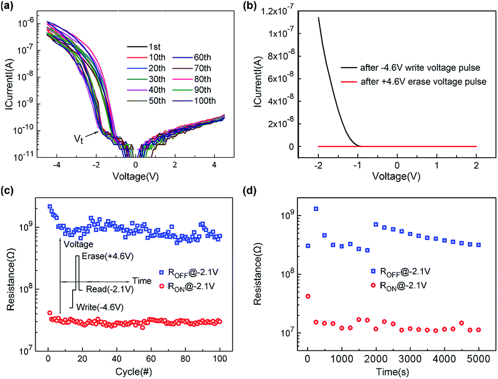 | ||
| Fig. 4 (a) Reproducibility of RS in bias sweeping mode of the Ag/BZO/SRO device for 100 continuous cycles (0 V → 4.5 V → 0 V → −4.5 V → 0 V); (b) I–V curves of the Ag/BZO/SRO measured after application of −4.6 V write and +4.6 V erase bias pulses. Pulse width is 1 ms; (c) fatigue performance of the BRS under 100 repetitive write/read/erase/read cycles. Inset is the configuration of one write/read/erase/read cycle. The bias for write, erase and read pulse are −4.6 V, +4.6 V and −2.1 V respectively. Pulse width is 1 ms; (d) data retention of the Ag/BZO/SRO device for HRS and LRS measured under constant readout bias within 5000 s. | ||
To check the modulation of resistive states under voltage pulses, a negative and positive voltage pulses (Vwrite = −4.6 V and Verase = 4.6 V) with 1 ms width were applied on the Ag/BZO/SRO device to achieve LRS and HRS, respectively. And then the current was measured at low reading voltage Vread (−2 V ≤ Vread ≤ 2 V). A good resistance state modulation of the device by the bias pulses is achieved, as seen in Fig. 4b.
Fatigue performance of the device was also tested by applying 100 repetitive write/read/erase/read cycles. As shown in the inset in Fig. 4c, −4.6 V write, +4.6 V erase and −2.1 V read bias pulses with widths of 1 ms were used. Reliable bistable RS is obtained. It can be seen that the resistance in the LRS has a narrow distribution than that of the HRS. The on/off ratio is typically one order of magnitude. Furthermore, the data retention of the device in HRS and LRS were measured under constant readout bias of −2.1 V within 5000 s, as shown in Fig. 4d. Apparently, the resistance values in both states are stable, indicating the nonvolatile and the nondestructive readout properties of the device.
Discussions
Normally, the stereotype conduction mechanisms for insulators23 can be grossly classified as the thermionic emission limited (TEL), Poole–Frenkel emission limited (PFL), Schottky emission, Fowler–Nordheim tunnelling, and the space charge limited (SCL) conduction mechanisms. These mechanisms can be distinguished via the logarithmic plot of I–V curve.It is well known that the PF and Schottky emissions can be characterized by linear  and
and  respectively, with J the current density. However, by replotting the I–V curves for the positive and negative bias sweep regions of Fig. 2 (see Fig. 5), no straight lines in both
  curves can be found as shown in the inset of Fig. 5, indicating that both PF and Schottky mechanisms can be ruled out.
 | ||
Fig. 5 ln![[thin space (1/6-em)]](https://www.rsc.org/images/entities/char_2009.gif) I–lnV curves of the Ag/BZO/SRO device: (a) positive bias and (b) negative bias regions. Arrows indicate sweeping sequence. Values of slopes are listed beside the lines. Insets are ln(J/V)–√V and lnJ–√V curves. I–lnV curves of the Ag/BZO/SRO device: (a) positive bias and (b) negative bias regions. Arrows indicate sweeping sequence. Values of slopes are listed beside the lines. Insets are ln(J/V)–√V and lnJ–√V curves. | ||
For the lnI–lnV curves, in the 0→8 V region of the positive bias sweeping (corresponding to the HRS), three different regimes are discriminated: two linear regions for lower (<0.7 V) and higher biases (>1.3 V) and a nonlinear increase region for the in-between biases. This is the well-known SCL current feature,24 and the bias values of 0.7 and 1.3 V denote the ohmic-boundary bias and the trap filled limit (TFL) onset bias respectively. As we know, electron traps formed by defects in films locate below the conduction band can absorb injected electrons. Such defects in oxygen-deficiency BZO films can come from oxygen vacancies.25 The intermediate region between the ohmic and TFL areas represents the transition between them, providing information about the trap distributions.26 Thus, the I–V characteristic is well described when assuming that the traps are exponentially distributed within the forbidden energy gap. Then the trap energy distribution function is given by26
 | (1) |
 | (2) |
Fig. 5 shows that the I–V characteristics transits from ohmic conduction to the TFL conduction directly without the SCL conduction as a transition part. This is because the trap distribution is deep enough.27 So with the increase of the voltage, quasi-Fermi level Ep rises and has already entered the trap distribution when the space charge limit is reached.
In the 8 → 0 V region of the positive bias sweeping (corresponding to the LRS), the slope of TFL region is lower than that in the HRS. According to eqn (2), the decrease of the TFL slope can be ascribed to the decrease of Et at constant temperature. We suggest that charge detrapping takes place and makes the quasi-Fermi level Ep shift away from the conduction band while still intersects the exponential trap distribution in HRS → LRS transition induced by external voltage bias. Schematic view of this process is shown in Fig. 6. Besides, we can note that when the sweeping bias begins to decrease at 8 V, the current increases. It can be viewed as an evidence of the charge detrapping process.
 | ||
| Fig. 6 Schematic diagram of the exponentially distributed density of states as a function of energy, N(E), at constant temperature. Evb and Ecb mark the edges of the valence and conduction bands, respectively. Et is the characteristic constant of the distribution, in which the N(Et) has been reduced by 1/e as compared with the N(Ecb). In the band gap, the area under the exponential distribution curve indicates the total trap density. Et shifts away from Ecb in the switching from HRS to LRS. | ||
According to the above analysis, we can conclude that the resistance switching induced by the external bias originates from the change of trap distribution. The resistance states are dependent on the carrier trapping levels in the films, namely the higher trapping level corresponding to HRS while the lower one corresponding to LRS.
Similarly, charge detrapping of carriers takes place during the HRS → LRS transition in the negative bias sweeping part, making the quasi-Fermi level Ep shift away from the conduction band and lowering the slope of the TFL region in the LRS. However, slope of the LRS part increases with decreasing voltage. It seems that some charge trapping process takes place. Besides, comparing Fig. 2 with Fig. 3c, we can see that the value of positive voltage affects the current under negative voltage greatly. So, interface states may be the reason.28
As is known, the TFL is regarded as a bulk limited conduction mechanism. However, the I–V curve shows great asymmetry which reveals interface limited conduction characteristics. These contradictions can be solved, if we assume that the TFL conduction occurs in the depletion layer of the Schottky contact.27
From Fig. 3, we can see that, the I–V curves under small V show hysteresis and opposite polarity between partial I and V. This can also be explained by the charge trapping/detrapping process.22 When BZO is negatively biased, as the absolute value of V increases, the carriers in the space charge layer are slowly emitted and redistributed. The polarity of the resulting current inside the insulator is the same as that of V. When the absolute value V is reduced, the carriers return to the initial positions. The polarity of the resulting current inside the insulator is opposite to V. The situation is the same when the BZO is positively biased. We should note that I can flow in the circuit without the carrier transporting across the Schottky barrier. Namely, due to an image charge effect, the carrier redistribution in the depletion layer changes the carrier concentration in the electrode and yields I in the measurement system. Therefore the carrier redistribution inside the BZO during the band bending can explain the relaxation current.
As V increases, a substantial fraction of I is expected to flow across the metal/BZO interface, and I–V characteristics asymmetric to V emerge.22 In this process, the electrons are emitted from traps in BZO, yielding a net increase of carriers density in BZO. If I is limited by the barrier of a sharp metal/insulator interface, the Schottky emission limited character is expected. Otherwise, the SCL or TFL in the depletion area is expected like in our sample. Besides, the asymmetry of the I–V curve is great. This great asymmetry could stem from the different interface structure. First, the top and bottom electrode materials are different. Second, the as-grown BZO film shows bi-layered structure, in which the top layer is polycrystalline while the bottom layer is monocrystalline.
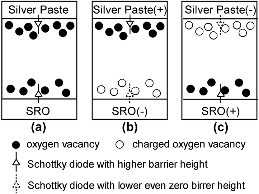
To exclude the effects of Ag on the RS effect,28 EDX analysis was performed on the Ag/BZO/SRO device with the ON state. Results are shown in the Fig. 7. The EDX line profile collected from across both SRO and BZO films concerning the intensity of Ag suggests that there are little Ag inside the film. So now we can comprehend the switchable diode effect behaviour as depicted in Fig. 8. The Ag/BZO/SRO device can be viewed as two back-to-back Schottky diodes (caused by interface Schottky barriers as well as interface states), in series with the BZO as a resistor. At the beginning, oxygen vacancies are distributed in the BZO. For clarity, only oxygen vacancies at the interface are drawn. When the device is under positive bias, the Schottky barrier at the ground interface limits the current flow and the device is in the HRS. With the increase of voltage, electrons trapped at the oxygen vacancies detraps due to the high voltage drop across the reversely biased Schottky barrier.14 Positively charged oxygen vacancies left at the interface can effectively lower the barrier height and turn the device into LRS. When the device is under negative bias, same process occurs at the opposite interface. The dynamic trapping and detrapping of oxygen vacancies modulate the interface Schottky barrier, leading to the switchable diode effect behaviour.
 | ||
| Fig. 7 (a) Cross section Z-contrast image of the ON-state device. (b) EDX line profiles collected from across both SRO and BZO films concerning the intensity of Ba, Sr and Ag. | ||
 | ||
| Fig. 8 Schematic illustration of the switching mechanism of Ag/BZO/SRO device. (a) The initial state. (b) Under positive sweeping voltage bias. (c) Under negative sweeping voltage bias. | ||
In the MFM structure, there are some controversies on whether the switchable diode effect is a general characteristic. L. M. Hrib et al.29 have stated that such behaviour may be present only if the polarization induced band bending at the interface is generating an accumulation layer. For example, the potential barriers are estimated to be about 0.6 eV for SRO/BiFeO3/Pt structure, while the band bending due to polarization can be as high as 0.8 eV. So the diode-like behaviour in this structure is switchable. Similarly, we can expect that such a rule can also apply to the non-ferroelectrics. However, the Schottky barrier modulation induced by charge trapping/detrapping in nonferroelectrics is much lower, as only around 0.08 eV in the Pt/Ba0.7Sr0.3TiO3/Pt planar device. As stated above, Schottky barriers at both interfaces of our Ag/BZO/SRO device are shallow. This could make possible the flattening of the interface potential barrier by charge detrapping, and therefore the occurrence of the switchable diode effect.
As for the improved retention data property, interface states may play an important role since it can trap the detrapped electrons from oxygen vacancies. Good retention behaviour via electrons trapping/detrapping by interface states has already been demonstrated in other systems.30,31 In our sample, the interface states may come from the grain boundaries32 as shown in the Fig. 1. Furthermore, the interface strain can also induce the change of the oxygen vacancy structures near the interface,33 which can significantly alter the physical properties of the as-grown films.
Conclusions
Oxygen deficiency BaZrO3 thin films were grown on SrRuO3-covered SrTiO3 (001) single crystals by pulsed laser deposition. Microstructure of the BZO film shows bi-layered characteristics, in which the bottom layer shows epitaxy while the top layer shows polycrystalline. Voltage–current characteristics and their reproducibility were tested for the BZO films. Results show that it has the switchable diode effect. The voltage–current relationship can be interpreted by the trap controlled space charge limited current theory which is regarded as a bulk limited conduction mechanism. The carriers trapping/detrapping has worked in this whole process by affecting the energy band bending and traps energy distribution at the metal/insulator interface. The current–voltage curves also show great asymmetry on transition voltage, indicating an interface limited conduction character. To solve this contradiction, we assume that the trapping/detrapping process occurs in the depletion layer at the metal/insulator interface. Besides, improved retention behavior is achieved, which may be related to interface states caused by the grain boundaries of the BaZrO3 films.Acknowledgements
This work is financially supported by US NSF Grant #8044081, and by the National Natural Science Foundation of China (No. 11427806). Also, Ding and Xu would like to acknowledge the supports from the “China Scholarship Council” for their PhD research at UTSA.References
- W. Haensch, E. J. Nowak, R. H. Dennard, P. M. Solomon, A. Bryant, O. H. Dokumaci, A. Kumar, X. Wang, J. B. Johnson and M. V. Fischetti, IBM J. Res. Dev., 2006, 50, 339 CrossRef CAS.
- S. D. Ha and S. Ramanathan, J. Appl. Phys., 2011, 110, 071101 CrossRef.
- S. Tehrani, J. Slaughter, E. Chen, M. Durlam, J. Shi and M. DeHerren, IEEE Trans. Magn., 1999, 35, 2814 CrossRef.
- S. Raoux, G. W. Burr, M. J. Breitwisch, C. T. Rettner, Y.-C. Chen, R. M. Shelby, M. Salinga, D. Krebs, S.-H. Chen and H.-L. Lung, IBM J. Res. Dev., 2008, 52, 465 CrossRef CAS.
- R. Waser and M. Aono, Nat. Mater., 2007, 6, 833 CrossRef CAS PubMed.
- J. F. Scott and C. A. P. De Araujo, Science, 1989, 246, 1400 CrossRef CAS PubMed.
- W. Zhuang, W. Pan, B. Ulrich, J. Lee, L. Stecker, A. Burmaster, D. Evans, S. Hsu, M. Tajiri and A. Shimaoka, Electron Devices Meeting, 2002. IEDM'02, International, San Francisco, 2002 Search PubMed.
- I. Baek, D. Kim, M. Lee, H.-J. Kim, E. Yim, M. Lee, J. Lee, S. Ahn, S. Seo and J. Lee, Electron Devices Meeting, 2005. IEDM Technical Digest. IEEE International, Washington, 2005 Search PubMed.
- Y.-C. Chen, C. Chen, C. Chen, J. Yu, S. Wu, S. Lung, R. Liu and C.-Y. Lu, Electron Devices Meeting, 2003. IEDM'03 Technical Digest, IEEE International, Washington, 2003 Search PubMed.
- A. Tsurumaki, H. Yamada and A. Sawa, Adv. Funct. Mater., 2012, 22, 1040 CrossRef CAS.
- Y. Guo, B. Guo, W. Dong, H. Li and H. Liu, Nanotechnology, 2013, 24, 275201 CrossRef PubMed.
- P. Blom, R. Wolf, J. Cillessen and M. Krijn, Phys. Rev. Lett., 1994, 73, 2107 CrossRef CAS PubMed.
- K.-j. Jin, C. Ge, H. B. Lu and G. Z. Yang, Nano-Micro Lett., 2013, 5, 81 CrossRef.
- X. Zou, H. G. Ong, L. You, W. Chen, H. Ding, H. Funakubo, L. Chen and J. Wang, AIP Adv., 2012, 2, 032166 CrossRef.
- C. H. Nieh, M. L. Lu, T. M. Weng and Y. F. Chen, Appl. Phys. Lett., 2014, 104, 213501 CrossRef.
- T. Maiti, R. Guo and A. Bhalla, J. Am. Ceram. Soc., 2008, 91, 1769 CrossRef CAS.
- M. Liu, J. Liu, C. Ma, G. Collins, C. Chen, A. D. Alemayehu, G. Subramanyam, J. He, J. Jiang and E. I. Meletis, CrystEngComm, 2013, 15, 6641 RSC.
- M. Liu, C. Ma, G. Collins, J. Liu, C. Chen, A. D. Alemayehu, G. Subramanyam, Y. Ding, J. Chen and C. Dai, Nanoscale Res. Lett., 2013, 8, 1 CrossRef PubMed.
- C. Chen, Y. Cao, Z. Huang, Q. Jiang, Z. Zhang, Y. Sun, W. Kang, L. Dezaneti, W. Chu and C. Chu, Appl. Phys. Lett., 1997, 71, 1047 CrossRef CAS.
- F. Zhang, Y. B. Lin, H. Wu, Q. Miao, J. J. Gong, J. P. Chen, S. J. Wu, M. Zeng, X. S. Gao and J. M. Liu, Chin. Phys. B, 2014, 23, 027702 CrossRef.
- E. Celik, Y. Akin, I. Mutlu, W. Sigmund and Y. Hascicek, Phys. C, 2002, 382, 355 CrossRef CAS.
- Y. Watanabe, Phys. Rev. B: Condens. Matter Mater. Phys., 1999, 59, 11257 CrossRef CAS.
- J. Simmons, J. Phys. D: Appl. Phys., 1971, 4, 613 CrossRef CAS.
- Y. Xia, W. He, L. Chen, X. Meng and Z. Liu, Appl. Phys. Lett., 2007, 90, 022907 CrossRef.
- M. F. C. Gurgel, M. L. Moreira, E. C. Paris, J. W. M. Espinosa, P. S. Pizani, J. A. Varela and E. Longo, Int. J. Quantum Chem., 2011, 111, 694 CrossRef CAS.
- P. Blom, M. De Jong and J. Vleggaar, Appl. Phys. Lett., 1996, 68, 3308 CrossRef CAS.
- D. S. Shang, Q. Wang, L. D. Chen, R. Dong, X. M. Li and W. Q. Zhang, Phys. Rev. B: Condens. Matter Mater. Phys., 2006, 73, 245427 CrossRef.
- Y. C. Yang, F. Pan, Q. Liu, M. Liu and F. Zeng, Nano Lett., 2009, 9, 1636 CrossRef CAS PubMed.
- L. M. Hrib, A. G. Boni, C. Chirila, I. Pasuk, I. Pintilie and L. Pintilie, J. Appl. Phys., 2013, 113, 214108 CrossRef.
- G. Yang, C. H. Jia, Y. H. Chen, X. Chen and W. F. Zhang, J. Appl. Phys., 2014, 115, 204515 CrossRef.
- C. H. Jia, X. W. Sun, G. Q. Li, Y. H. Chen and W. F. Zhang, Appl. Phys. Lett., 2014, 104, 043501 CrossRef.
- S. Y. Chung, I. D. Kim and S. J. Kang, Nat. Mater., 2004, 3, 774 CrossRef CAS PubMed.
- W. Donner, C. Chen, M. Liu, A. J. Jacobson, Y.-L. Lee, M. Gadre and D. Morgan, Chem. Mater., 2011, 23, 984 CrossRef CAS.
| This journal is © The Royal Society of Chemistry 2016 |