Stuart R. Thomasab,
Chia-Wei Chenb,
Manisha Dateb,
Yi-Chung Wangb,
Hung-Wei Tsaib,
Zhiming M. Wang*a and
Yu-Lun Chueh*b
aInstitute of Fundamental and Frontier Sciences, University of Electronic Science and Technology of China, People's Republic of China. E-mail: zhmwang@gmail.com; ylchueh@mx.nthu.edu.tw
bDepartment of Materials Science and Engineering, National Tsing Hua University, Hsinchu 30013, Taiwan
First published on 27th May 2016
Chalcopyrite materials, in particular CuInS2 (CIS), CuInSe2 (CISe) and Cu(In,Ga)Se2 (CIGS), have drawn significant attention recently owing to their highly advantageous optoelectronic properties, making them well suited to their best known application in solar cells. In this review, we will introduce some of the recent advances in the field of chalcopyrite nanostructure synthesis and discuss the further benefits these nanostructured materials offer over their thin-film and bulk counterparts. We will highlight a number of synthesis methods that utilize both physical and chemical based techniques, encompassing vacuum, solvothermal and solution based approaches. The conclusion will briefly highlight some of the challenges that we are yet to overcome, whilst reiterating the benefits that nanostructured chalcopyrites have to offer.
The first reference to the use of chalcopyrite materials in photovoltaic applications was presented by Wagner et al. in 1974 where a CISe single crystal was used as a p-type absorber in conjunction with an n-type CdS layer, and a transparent window layer, forming a heterojunction photovoltaic detector. In general, this has remained as the basic structure for chalcopyrite based solar cell devices. The deposition of these materials rely primarily on sputtering, co-evaporation or solution based deposition of metallic precursors followed by a selenization step at high temperature in the presence of a hydrogen selenide gas, or other source of S/Se vapour, where crystallization of the final thin-film takes place. Whilst these methods generally provide the best strategy for large-area thin-film growth, production volume scaling remains challenging due to difficulty in forming homogeneous films, the use of toxic gasses and materials, and costly vacuum processing methods. The growth of nanostructured chalcopyrites can be achieved using a much wider variety of processing methodologies. In this review we present a range of top-down, bottom-up approaches, solvothermal, template assisted growth, microwave assisted, and colloidal based approaches, and many more. For a more general overview of the field of chalcopyrite material properties, solar cells and other related applications we direct the reader to a range of excellent articles.5,10–14
The chalcopyrite materials under discussion here are direct transition bandgap p-type semiconductors with optical properties that make them well suited to optoelectronic applications. The name chalcopyrite is taken form the mineral CuFeSe2 that crystallizes in the tetragonal crystal system space group I2d as shown in Fig. 1(a). Whilst these I–III–VI2 ternary compounds and their quaternary alloys cover a broad range of material systems we primarily focus here on CuInxGa1−xSe2 and CuInxGa1−xS2 systems. The crystallographic parameters reported previously for the ternary parent materials systems are summarized in Table 1.15,16 In the quaternary mixed alloy systems, the lattice constants, a and c, are observed to change linearly in relation to x, with a composition of x = ∼0.8 seen to achieve the ideal c = 2a ratio.17–20 Although X-ray diffraction (XRD) analysis provides a useful tool for correlating processing parameters with structural composition, the co-existence of impurity phases within CIGS material systems can be difficult to differentiate. Stacking fault densities and dislocations along the [112] crystal plane are known to occur in Cu-poor CuInS2 films.21 Additionally, extrinsic alkali dopants are commonly employed in solar cell applications in order to enhance performance.22,23 As a result, the chemical and structural details of such films must be confirmed in detail. Typically, secondary ion mass spectroscopy (SIMS), scanning electron microscopy (SEM), transmission electron microscopy (TEM), X-ray energy dispersive spectroscopy (EDS), X-ray photoelectron and convergent beam electron diffraction (CBED) techniques used.24–27
The interface/surface properties of bulk chalcopyrites are of significant importance in solar cell applications. For example, MoSe2 formation at the interface between the Mo contact and the CIGS, during high temperature selenization of the CIG precursor is commonly observed via TEM, and is known to help form of a high quality ohmic contact.28,29 At the front interface between the CIGS and CdS fewer issues are observed as the CdS layer it typically deposited at room temperature, however elemental mixing has been observed and passivation treatments of the CIGS films have been demonstrated to enhance device performance.30–32 The substrate surfaces on which nanostructures are grown, as well as the interface properties between nanostructures and their growth environment all play a significant role during nucleation and crystal growth.33,34 As you will see, many of the reports outlined in this text take advantage of templated growth techniques and surface modification methods to create and control ordered nanostructured materials.
The composition in CuInxGa1−xSe2 and CuInxGa1−xS2 systems also has a significant effect on the materials optical bandgap with values between ∼1.0 and ∼1.6 eV achievable by varying x.17 By carefully tuning the chosen deposition method, this advantageous property can be used to grade the bandgap as a function of depth within photovoltaic devices, enabling optimised absorption, and charge generation and separation properties.35–37 Their high optical absorption coefficient, in the region of 10−5 cm−1 for energies greater than the bandgap are one of the key properties that make them highly applicable for use in lightweight and flexible thin-film (typically <1.5 μm) solar cells,38–41 whilst low susceptibility to proton and electron radiation also make these materials potentially useful for space applications.42,43
Nanoscale, or low dimensional (low-D), materials are generally considered as those having dimensions confined to the 100 nm scale length or below in at least one dimension. At such small length scales size-dependent properties become observable. Such effects have long been exploited by nature for their wetting and photonic properties, and their use in modern materials science can be highly advantageous depending on the chosen material and its application.44 Surface plasmon resonance effects in certain metal particles are of particular interest in optical/optoelectronic fields, where careful consideration of size, shape and periodicity makes it possible to significantly alter their non-linear, interference, refraction, absorption, emission and diffraction properties.45,46 Quantum confinement in semiconductor systems is observed when material dimensions approach that of the de Broglie wavelength of the electron wave function. Such confinement leads to a discrete energy structure and a characteristic widening of the semiconductors bandgap. Quantum confined structures are utilised in a wide range of applications for both their enhanced optical and charge transport properties. Examples include quantum dot solar cells, light emitting diodes (LEDs), and super-lattice/quantum well structures that are used in transistor and resonant tunneling diode (RTD) applications.47–52 Understanding the phase related properties of low-dimensional materials is also of great importance. Transition metal di-chalcogenides (TMDs) are one category of low-D materials that are currently being investigated for use in a range of device applications, where phase transitions lead to a corresponding change between metallic and semiconducting behavior.53 As an example, selective formation of metallic phases at the device contact area has been utilised to enhanced charge injection between metallic contacts and the semiconducting phase.54 The thermal and mechanical properties of nanostructures can be highly diverse depending on the material in question. The melting temperature of Au nanoparticles is well known to reduce significantly with decreasing diameter.55 The yield strength of some nanoscale metals are known to increase dramatically with decreasing feature size, whilst the extraordinary mechanical properties of graphene are currently one of the most intensively researched fields.66–69 Additionally, the inclusion of nanostructures, such as nanowires into thin-films, and the use nanopatterning techniques have also been demonstrated as efficient ways of improving the mechanical robustness of solar cell devices.39,70 The chemical activity of nanostructured materials can be enhanced significantly by alteration of their size and shape properties. By increasing their surface area to volume ratio, a greater number of chemically active surface sites can be exposed. Layered materials such as TMDs are also quite unique materials that can possess chemically active sites confined to edge sites or grain boundaries, whilst their basal planes remain relatively inert. The chemical properties of these structures and materials are currently being investigated for use in wetting, catalytic, water splitting and battery applications.71–77 Whilst much of the work addressed in this review utilizes many of these interesting structure–property related phenomenon, it is the aim of this review to focus on the synthesis processing. However, where relevant, we briefly highlight any such points of interest, whilst further details can be found in the referenced material.
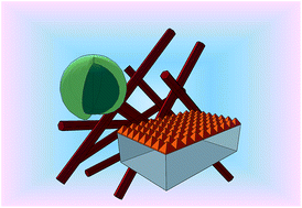
The materials under discussion in this review are categorized into three main classes; 0-dimension materials such as nanoparticles or nanocrystals; 1-dimension materials such as nanorods and nanowires; and a third, broader term, low-dimensional materials, in reference to nanocones, nanotips and nanorippled type structures. In each section we will highlight some of the latest methodologies employed in their fabrication and also discuss their use in current areas of research. Finally, we will offer a short conclusion and outlook.
Structure | Chemical composition | Processing method | Application | Ref. |
---|---|---|---|---|
Nanoparticles | CuInGaSe | Solution processed, spray deposition and annealing under a selenium atmosphere | Solar cell | 56 |
CuInS2, CuInSe2, CuGaS2 | Solution processed | N/A | 57 | |
CuGaSe2, CuInSe2, Cu(InGa)Se2 | Solution processed, powder Se source | Photo-response measurement | 58 | |
CuInSe2 | Solution processed | Solar cell | 59 | |
CuInSe2 | Solution processed | Photodetector | 60 | |
Metal-decorated nanoparticles | Au–CIGS side-by-side | Solution processed, using HAuCl4·xH2O as Au-source | N/A | 61 |
Au-decorated CuInS2 | Solution processed, using HAuCl4·xH2O as Au-source | Distillation | 62 | |
Core–shell nanoparticles | Au-core/CIGS-shell | Solution processed, selenourea as Se source and HAuCl4·xH2O as Au-source | N/A | 61 |
Au-core/CIGS-shell | Solution processed | Photoluminescence | 63 | |
CuInS2/ZnS core/shell | Solution processed | In vivo biological imaging | 64 | |
CuInS2/ZnS core/shell | Solution processed | In vivo local acute toxicity | 65 |
In 2008, Guo, et al. designed a facile inorganic CISe2 nanoparticle ink utilising only one solvent, oleylamine, to fabricate CISe2 nanoparticle based solar cells.84 They first increase the temperature of oleylamine to ∼130 °C, following which, they added the CuCl, InCl3 and Se precursors to the oleylamine and further raised the temperature to 265 °C for 1 hour, forming CISe2 nanoparticles. Following nanoparticle formation, the temperature was reduced to 60 °C with the introduction of additional ethanol and hexane for washing and centrifugation steps. After centrifugation the precipitated CISe2 nanoparticles were re-dispersed in toluene forming a CISe2 ink. The nanoparticle ink was then drop cast onto Mo coated soda lime glass (SLG) and then annealed at 500 °C to remove organic byproducts and sinter the film. 50 nm CdS, 50 nm i-ZnO and 300 nm ITO films were deposited successively for cell fabrication. The final CISe2 solar cell exhibited a PCE of 3.2%. Whilst these values are not the highest, they do outline a methodology that allows close control of the chalcopyrite structure that may offer a route to further enhanced device performance.
Wang et al. proposed an interesting hybrid structure (Fig. 2(a)) utilising CuInSe2 nanocrystals and poly(3-hexylthiophene) (P3HT) (Fig. 2(b)), a π-electron conjugated polymer with a high visible-light absorption coefficient, for use in photodetector applications.60 As charge carriers are excited by the incident light, electrons transfer to the CuInSe2 nanoparticles due to its higher electron affinity when compared to the P3HT (Fig. 1(c)). Conversely, the holes transfer to the P3HT. The absorption of the hybrid CuInSe2–P3HT is significantly enhanced in comparison to the CuInSe2 nanocrystals or pure P3HT film when measured in isolation (Fig. 2(d)). In addition, the on/off ratio is significantly enhanced when observing the photocurrent response, resulting from the energy-level offset between the CuInSe2 and P3HT film as shown in Fig. 2(e). The nature of the nanocrystal and polymer matrix creates charge transport routes that allow the charge carriers to reach their electrodes with reduced recombination losses due to the better charge separation, in turn leading to better device performance.
![]() | ||
Fig. 2 (a) Schematic of hybrid photodetector structure, (b) chemical structure of P3HT, (c) pathways of photo-excited electrons and holes, (d) UV-visible absorption spectra for CuInSe2 nanoparticles, P3HT film and hybrid CuInSe2–P3HT film, and (e) on/off switching current behavior of photodetector at incident light intensity of 7.63 mW cm−2 and a bias voltage of 0.4 V. Reprinted with permission from ref. 60. |
In 2011, Xu et al. demonstrated an approach toward the synthesis of heterostructured Au-decorated CIGS nanoparticles.88 The CIGS nanoparticles were fabricated using CuCl, InCl3, Ga(NO3)3·9H2O in oleylamine and heated to 120 °C to purge oxygen and water from the solution. Se was then added when the temperature reached 240 °C to enable the synthesis of the CIGS nanoparticles. The precipitated CIGS nanoparticles were then re-dispersed in chloroform and centrifuged to remove any excessively large nanoparticles. The supernatant was then heated to ∼62 °C and HAuCl4·xH2O was introduced into the system as an Au-source. The reaction was carried out for 5 hours forming Au nanocrystals on the side of the CIGS nanoparticles. Low magnification and high resolution TEM images are shown in Fig. 3(a) and (b) where crystallized Au is found to attach predominantly to the (112) surfaces of the CIGS nanoparticles. The polar (112) surface is comprised of Cu/In or Se layers, and the Au tends toward forming an Au–Se bond when the Se layer is the termination plane (Fig. 3(b)).89,90 Moreover, the lower surface energy of the (112) plane will consume less energy during the growth of Au.88
![]() | ||
Fig. 3 Low-magnification TEM image (a) and high-resolution TEM image (b) of the Au-decorated CIGS nanoparticles, (c) absorption spectra for pure Au nanoparticles and pristine CuInS2 nanoparticles and (d) absorbance spectra and enhancement factor of the Au-decorated CuInS2 nanoparticles and Au–CuInS2 mixtures. Reprinted with permission from ref. 64, 89, and 90. |
A similar experimental process was also used for Au-decorated CuInS2 formation and applied for selective distillation in non-polar solvent systems by Yen et al.62 They synthesized CuInS2 with CuCl, InCl3 and S powder in oleylamine and introduced HAuCl4·3H2O to form Au-decorated CuInS2 nanoparticles.62 Fig. 3(c) shows the absorbance of pure Au nanoparticles with an absorption peak at ∼520 nm and pristine CuInS2 nanoparticles with lower absorption at visible and infrared wavelengths. Fig. 3(d) shows the moderately enhanced absorbance after mixing the Au and CuInS2 nanoparticles together in solution. Moreover, the heterostructured nanoparticles results in a further improved absorbance compared to the Au–CuInS2 mixture or constituent nanoparticles alone. The results of 2D Finite-Difference Time-Domain (FDTD) simulations indicated that both Au-decorated CuInS2 and Au–CuInS2 mixture possess high electromagnetic intensity due to surface plasmon resonance (SPR), with the electromagnetic intensity of the Au-decorated CuInS2 being much stronger than the Au–CuInS2 mixture because of the induced charge transfer and higher refractive indices resulting from the intersecting electron states.91,92 With the intensified absorption in the range of 550–800 nm, corresponding to the highest intensity of the solar spectrum, the Au-decorated CuInS2 nanoparticles are able to increase the conversion efficiency of the thermal energy generation achieved during the distillation of methylcyclohexane (MCH) with toluene.62 The polarity of MCH is closer to that of the Au-decorated CuInS2 nanoparticles than toluene, enabling the Au-decorated CuInS2 to attract the MCH readily via dipole interactions. Through bonding with the high thermal energy conversion efficiency material, MCH becomes easier to vaporize than toluene, and strengthens the selectivity of distillation.93 Thus it is possible that the combination of metals, which can provide plasmonic effect enhancement, and high absorption coefficient chalcopyrite nanoparticles, can be highly beneficial to other thermal energy generation approaches.
Although the performance of CIGS solar cells is approaching that of Si-based solar cell, cost is still an issue due to the use of indium (In).94 Thinning the absorber layer by combining plasmonic metals and CIGS in solar cells is one approach toward reducing production costs whilst maintaining the high absorption performance.80 Aside from plasmonic metal-electrodes and direct contact plasmonic metals, CIGS heterostructured Au–CIGS core/shell nanoparticles can significantly increase the intensity of the electric field. Xu et al. have successfully synthesized Au–CIGS core–shell nanoparticles by reacting Cu(acac)2, In(acac)3, Ga(acac)3 in oleylamine and dichlorobenzene, followed by heating at 120 °C to purge oxygen and water from the solution.88 HAuCl4·xH2O was injected into the solution and the system kept at 120 °C for 10 minutes to promote Au seed nucleation. Finally, selenourea was utilised as a Se source, after which the CIGS would nucleate on the Au seeds to form a CIGS shell surrounding the Au core. Due to the spherical shape of the Au nanoparticles, uniform surface energy on the Au surface results in multiple nucleation sites, which contribute to the growth of a high quality CIGS shell. In turn, enhanced absorption was found in the range of 600–900 nm, matching the highest intensity region of the solar spectrum making them ideal for light harvesting applications.88
Chalcopyrite nanoparticles with their direct band gap can also be developed as color-tunable emitters with a broad color window, ranging from visible to near-infrared regions.81 Moreover, the performance of the emitter can be enhanced with the help of a ZnS shell surrounding the semiconductor core.95 Xie et al. proposed the synthesis of CuInS2/ZnS core/shell nanoparticles by introducing zinc stearate into the growth solution of CuInS2 nanoparticles at 80 °C.63 The temperature was then increased to 210 °C and maintained for 30 minutes forming ZnS shell. Following the formation of the ZnS shell, the photoluminescence (PL) quantum yield increased from ∼3% to ∼30%. Fig. 4(a) shows the observed blue-shift in the PL peaks corresponding to decreasing CuInS2 nanoparticle size, permitting the PL properties to be tuned over the visible to near-infrared region. In comparison to the more commonly discussed II–VI and IV–VI quantum dots, which contain heavy metals such as Cd, Pb or Hg, these CuInS2/ZnS core/shell nanoparticles can significantly reduce the environmental and health risks, making them suited to a much wider range of bio-related applications.
![]() | ||
Fig. 4 (a) Size dependent photoluminescence spectra for increasing size of CuInS2 nanoparticles, (b) fluorescence images obtained from mice injected with CuInS2/ZnS nanoparticles and (c) weight of RAIL and RATLN lymph nodes following different inject doses of toxic CdTeSe/CdZnS nanoparticles and non-toxic CuInS2/ZnS nanoparticles. Reprinted with permission from ref. 63, 64 and 96. |
Li et al. fabricated CuInS2/ZnS core/shell nanoparticles for bio-imaging applications, demonstrating the first instance of these nanoparticles used for in vivo imaging, mitigating the toxicity issues related to the use of conventional quantum dots that use heavy metals.96 Following the introduction of CuInS2/ZnS nanoparticles into mice, they were able to detect a fluorescence signal for 24 hours, observing stable vital functions within the host as shown in Fig. 4(b). Pons et al. have also utilized CuInS2/ZnS core/shell structure for sentinel lymph node imaging and compared their toxicity with CdTeSe/CdZnS core/shell nanoparticles.65 They recorded the comparative NIR fluorescence images of the right axillary lymph nodes (RALN) and right lateral thoracic lymph nodes (RLTLN), using both heavy-metal-based nanoparticles, and CuInS2/ZnS core/shell nanoparticles. Increased weight and inflammation of the RALN and RLTLN was used to indicate an induced immune response following nanoparticle injection. When using the same injected dose of both CdTeSe/CsZnS and CuInS2/ZnS core/shell nanoparticles, the weight of the RALN and RLTLN is much higher in the CdTeSe/CsZnS core/shell case, as shown in Fig. 4(c) and (d). The released Cd+ ions can accumulate in the organs, taking a longer time for metabolism. This work is strong indicator that CuInS2/ZnS core/shell nanoparticles are suitable for further investigation in safe bio-applications.
Structure | Chemical composition | Processing method | Application | Ref. |
---|---|---|---|---|
Nanorods and nanotubes | CuInS2 | Elemental solvothermal reaction | NA | 100 |
Nanorods | CuInS2 and AgInS2 | Single molecule precursor solvothermal process | NA | 107 |
Nanorods | CuInSe2 | Solvothermal reaction | NA | 102 |
Nanorods | CuInSe2 | Indium intercalated solvothermal approach | NA | 108 |
Nanorods | CuInS2 | Solvothermal reaction | NA | 104 |
Nanorods | CuInS2 | Colloidal solution-phase growth | NA | 105 |
2D, 3D nanorods | CuInGaS2 | Chemical growth | NA | 106 |
Nanorods | ZnS–CuInS2 | Non-injection colloidal method | Photo catalyst for RhB degradation | 109 |
Nanorod arrays | CuInSe2 | Template-assisted electrodeposition | NA | 110 |
Nanorod arrays | CuInSe2 | Template-assisted mechanical approach | NA | 111 |
Nanorod arrays | CuInS2 | Template-assisted nano casting approach | NA | 112 |
Nanorod arrays | CuInSe2 | Template-assisted nano casting approach | NA | 113 |
Nanorods and networks | CuInS2 | Phosphine-free colloidal method | NA | 114 |
Nanorods | CuInS2–ZnS | Heating-up method | NA | 115 |
Nanorods | CuInS2 | Organic molten salt method | NA | 116 |
Nanorods | CuInS2 | Microwave heating | NA | 117 |
Nanowires | CuInSe2 | Au-catalyzed VLS growth | NA | 118 |
Nanowires | CuInSe2 | VLS growth and annealing | Single-NW solar cell | 119 |
Nanowire arrays | CuInSe2 | Template-assisted electrodeposition | NA | 120 |
Nanowire arrays | CuInSe2 | Template-assisted electrodeposition | NA | 121 |
Nanowire arrays | CuInSe2 | Template-assisted electrodeposition | NA | 122 |
Core–shell nanowire bundles | CuInSe2/CuInS2 | Chemical approach | NA | 123 |
Nanowires | CuInSe2 | Solution phase synthesis | NA | 124 |
Nanowires | CuInS2 | Solution process | Photo response | 125 |
Nanowires | CuInS2 | Microwave-assisted SLS synthesis | NA | 126 |
Solvothermal/hydrothermal processing occurs in a closed environment offering precise control over the fabrication of nanostructured material properties, and has proven to be a widely useful processing method.98,99 Jiang et al. reported the formation of CuInS2 nanorods (NRs) using elemental precursors with ethylenediamine by direct solvothermal reaction at 280 °C for 24 h.100 They have studied the effect of liquid In and the solvent ethylenediamine on the growth process of the 1-D nanoscale CuInS2 NRs. The Solid–liquid–solid (SLS) growth mechanism of NRs was attributed to the presence of liquid In and the coordinating ability of ethylenediamine, which play important roles in the electron-transfer reaction and the growth of 1-D nanocrystallites. CuInS2 NRs were synthesized from an optimised mixture of In(S2CNEt2)3 and Cu(S2CNEt2)2 in ethylenediamine at 195 °C for 12 h by solvothermal processing through removal of the thione groups.101 This work resulted in the development of a new strategy of using nucleophilic attack to cut off the unnecessary parts of single-molecular precursors for the synthesis of CuInS2 NRs where ethylenediamine plays an important role. Similarly, Yang et al. have demonstrated a solvothermal synthesis method to create single-crystalline CuInSe2 NRs 50–100 nm in diameter and up to a few micrometers in length, with a direct band gap of 1.05 eV.102 The powder precursors were dissolved in ethylenediamine and kept at a reaction temperature of 120 °C. The growth of NRs started from the chelated-complex formation of [Cu(H2NCH2CH2NH2)2]+, which acts as a molecular template to combine with InSe2− toward the further growth of NRs. Detailed photoluminescence (PL) analysis of the NRs measured at 10 K shows seven groups of transitions characterized as bound excitons, free excitons, conduction band to acceptor levels, and bound excitons at different defects levels.
Fu et al. reported an interesting intercalation type solvothermal preparation method for CISe2 NRs by using as-prepared Cu2−xSe NRs with a diameter of about 300–500 nm as a precursor. This was followed by a reaction with indium chloride in ethylenediamine.103 A phase conversion occurs within the In3+ intercalated Cu2−xSe:In during the reaction which leads to the formation of CuInSe2 NRs.
From the reaction of aqueous solutions of CuCl2, In, CS2, and NaOH at a low temperature of 180 °C, Xiao et al. synthesized ternary CuInS2 NRs with lengths of 400–450 nm and diameters of 20–25 nm.104 At that reaction temperature, the melting of the metal particle provides an energetically favorable site for the reactants absorption, which increases the growth rate of NRs significantly. The process is considered a solution–liquid–solid (SLS) growth mechanism, within which, the formation of CuInS2 NRs, the reaction temperature and liquid In are all shown to play an important role.
Synthesis of wurtzite CuInS2 NRs consisting of hexagonal chalcocite Cu2S and wurtzite CuInS2, has been demonstrated utilising colloidal solution-phase growth at 260 °C by Connor et al.105 The growth process is initiated with nucleation of Cu2S nanodisks (NDs) with diameters of 22 nm and a thickness of 9 nm, accompanied by epitaxial overgrowth of CuInS2 NRs on one side of Cu2S NDs resulting in biphasic heterostructured Cu2S–CIS NRs. Above 250 °C, biphasic NRs are easily converted to tapered monophasic NRs due to fast diffusion of Cu(I) ions in the superionic state and their similar crystal structures. Furthermore, the direct assembly of CIGS NRs into highly ordered 2D and 3D superstructures by solution process has been reported by Singh et al.106 The spontaneous assembling of thiol capped NRs into 3D aligned NR clusters over a period of hour's shows end to end and side to side order. From Fig. 5(a) and (b), we can see that the aligned CIGS NR clusters form a hexagonal close packed (hcp) packing system with 11 ± 0.5 nm in width, 24 ± 1 nm in length and a d-spacing of 0.318 nm. From high-resolution top-view TEM images as shown in Fig. 5(c), a monolayer of vertically assembled thiol/amine capped CIGS NRs can be seen where NRs become self-aligned using an optimized concentration of 5 × 10⁻⁵ mol L−1. The clusters disassembled by ligand exchange with an amine and assembled either at the substrate interface or as free floating 2D sheets by directed assembly protocols. The authors consider this process to be chemically tunable and extendable over device scale areas.
![]() | ||
Fig. 5 (a) HRSEM image showing side-by-side alignment of nanorods in individual aligned nanorod clusters, (b) low-resolution angular dark-field STEM (DF-STEM) of monodispersed CIGS nanorods with inset HRTEM image of nanorod and (c) top down TEM image showing monolayer sheet of vertically assembled CIGS nanorods. Reprinted with permission ref. 106. |
CuInSe2 NR arrays can be deposited using a variety of templated growth techniques. One such method, demonstrated by Zhang et al. uses a tungsten/silicon rigid substrates with a porous anodic alumina (PAA) growth template, using electrodeposition where the pH was maintained at a value of 2.110 Following annealing at 450 °C in vacuum, the formed NRs were dense and compact with diameters of ∼100 nm, a length of ∼1 μm, and a resultant aspect ratio of ∼10. Further examples of templated growth have been demonstrated by Pashchanka et al. They employ a nano-casting template fabricated from porous polycarbonate films. The CIS2 NRs with pore diameters of 70–160 nm and length of 3.5–4.5 μm were fabricated using molecular copper and indium oximato complexes, and thiourea as single-source precursors.127 The NRs exhibit good stability and crystallinity after a final calcination step at 550 °C. This nano-casting approach generates well-separated and aligned NR bundles of CIS2 with controllable Cu/In/S ratio with a high yield and surface uniformity. A similar method has been utilised to fabricate high purity and crystalline, 3D CISe2 NR arrays, again using polycarbonate hard template by the same authors.128 Molecular precursors of copper and indium ketoacidoximato complexes and selenourea were used, enabling a high level of homogeneity of the NRs. In this work, porous films with pore diameters of 100 nm and 5 μm lengths were used for infiltration by the precursor solution in an inert atmosphere. CISe2 NRs with a bandgap of 1.03 eV displayed moderately improved absorption in the near-UV region and better absorption covering the whole visible range and a part of the near infrared range also.
Li et al. developed a low-cost and phosphine-free injection method for synthesis of CIS2 NRs.129 The reactivity of the monomers, and thus the size of copper sulfide seeds formed are influenced by the amount of oleic acid used. During the growth process of the NRs, larger seeds lead to the formation of hybrid CuS–CIS2 NCs as intermediates whereas smaller seeds were converted to CIS NRs. At high temperature, the reaction between oleylamine and oleic acid became the crucial factor to stimulate the bonding of NRs to multipods and networks. A modified technique using an extended heating method was employed by the same author, enabling the formation of CuInS2–ZnS NRs with controllable Zn content, where the mixture of oleylamine and oleic acid was used as a solvent.130 In this work the growth of alloyed ZnCIS NRs was initiated with the formation of copper sulfide seeds, which were further converted to CuInS2–ZnS by incorporation of indium and zinc ions.
A more environmentally friendly approach to CIS NR growth has been demonstrated by Zhang et al. utilizing an organic molten salt (OMS) method for the synthesis of CuInS2 NRs with lengths and diameters of about 700 nm and 40 nm respectively.116 The yield of the stoichiometric product prepared at 200 °C was between 75 and 85%, with the formation of CuInS2 NRs. Comparison between the absorption spectrum and the PL spectrum showed a redshift, which is attributed to a large Stokes shift in the NRs, indicating size related quantization effects. Utilizing a low-cost and quick microwave heating method in a deep eutectic solvent, the same authors demonstrated the fabrication of CIS2 NRs with diameters of 40 nm and lengths of 400 nm.117 During the formation of CuInS2 NRs the molecules are selectively adsorbed on the surface of CuInS2 seeds. The as-prepared CuInS2 NRs display strong light absorption across the entire visible light region to beyond 1100 nm. The as-prepared CuInS2 NRs exhibited a strong PL emission peak at 580 nm under an excitation wavelength of 366 nm.
![]() | ||
Fig. 6 (a) Four-step synthesis scheme for the production of single crystalline CIS nanowires, (b) TEM dark field image, formed in the 112 zone and (c) SEM image of CIS single nanowire solar cell device following completed fabrication. Reprinted with permission from ref. 119. |
Hung et al. developed a method to form CISe2 NW arrays utilizing a template-assisted pulse electrodeposition method in an acid-aqueous electrolyte, containing DMSO as a non-toxic additive, and using an AAO template.122 The CISe2 nanowires deposition was primarily controlled by the kinetics-driven growth operation within the electrolyte. The growth of NWs took place in a thermodynamic non-equilibrium state, and the observed 3D island morphology was not perceived to be influenced by the DMSO in the electrolyte. From photo-electrochemical (PEC) measurements, CISe2 NWs prepared using the DMSO containing electrolyte displayed an enhanced photocurrent response compared to those prepared using an electrolyte without DMSO.
The formation of CuInSe2 NWs by solution-phase synthesis without using metal nanocrystal catalysts has been demonstrated by Wark et al.124 By changing the relative amount of strong and weak binding surfactants to passivate the surface, CuInSe2 nanostructures varied from spheres to highly anisotropic NWs, with a saw-tooth morphology stack of truncated tetrahedrals achievable. In this case, weakly binding dioctylphosphine oxide (DOPO) played a significant role in the anisotropic 1-dimensional growth of CISe2 NWs. Additionally, Li et al. synthesized single-crystalline CuInS2 NWs with enhanced photo-responsivity, using this solution process through Ag2S catalyzed growth.125 Initially, Ag2S nanocrystals formed, which act as catalysts for the growth of the CuInS2 NWs. The high mobility of Ag+ can boost the creation of Ag+ vacancies in Ag2S, which alleviates the diffusion of Cu and In species from solution into Ag2S, reaching supersaturated states for the growth of the wurtzite CIS2 NWs.
Finally, Krylova et al. introduced a microwave-assisted solution–liquid–solid (MASLS) method for the formation of single-crystalline CuInS2 NWs via an eutectic growth mechanism including an overheated alloy catalyst.126 Using the MASLS method, high quality CuInS2 NWs can be synthesized with diameters of less than 10 nm. Growth can occur at a fast rate of 33 nm s−1, to lengths of 10 μm in less than 10 min, resulting in a high mass yield of 31%. The NWs length was irradiation time dependent, whereas the NWs diameters were complexly related to the precursor concentrations. The microwave irradiation is observed to overheat the liquid catalyst, which improves the solubility of Cu, In, S and reduces the supersaturation of CuInS2, thus assuring the two-dimensional growth of the crystal abates crystal nucleation, leading to the deposition of CuInS2 on the end of NW.
![]() | ||
Fig. 7 (a) SEM images of 400 eV Ar+ sputtered CIGS thin-films utilising incident angle of 90° for 30 minutes and (b) with 1 keV Ar+ irradiation for 10 minutes with radio frequency bias of −600 V. Inset images show the cross-sectional view. (c) AES elemental mapping of CIGS nanotips arrays showing Cu, In, Ga and Se composition and (d) TEM image of CIGS nanotips. Inset images show the HRTEM image and corresponding SAD pattern. Reprinted with permission from ref. 137, 147 and 148. |
Ion-induced roughening on the surface of targets after ion sputtering have been observed since the 1960s.139 The formation mechanism of ripple structures due to low energy ion sputtering have been proposed based on instability models, depending on the substrate temperature and the ion flux, such as the Bradley–Harper model140 and the Ehrlich–Schwoebel model,141 which result from the competition between; roughening due to the difference in sputter yield related to the surface curvature, and smoothening due to the ion induced surface diffusion. Likewise, nanodots and/or sharp nanocones have been observed on silicon142,143 and III–V semiconductors144,145 following ion sputtering. This method is gaining increasing attention as a way of forming such structures. Interestingly, nanotips tend to tilt with the incident angles, which cannot be explained by the instability models. A self-masking effect due to the surface segregation of the masking component is proposed as an explanation for such phenomena.146 The formation mechanism of CIGS nanotips can be explained by the mechanisms of surface segregation of the masking layer because the tilted CIGS nanotips become aligned with the incident angle of Ar+ ions. As shown in the Fig. 7(c), the masking material was found to be the segregated Cu-rich Cu2Se phases as a result of lower phase formation energies,147,148 which will act as the masking material for the CIGS inside the core of the tip, and thus result in the anisotropic etching behavior. The crystallinity also plays an important role of the formation of CIGS NTRs, as only the crystalline CIGS forms nanotips, and no ion induced amorphization of the surface was observed, as shown in Fig. 6(d). These CIGS nanotips arrays are ideal for solar cell applications due to their outstanding anti-reflection ability. However, the surface composition will change during the process due to segregation of Cu-rich phases, and thus additional post treatments either by etching in KCN solution or rapid thermal annealing are required.136 In comparison, wet etching methods may offer a better method to form stoichiometric CIGS nanostructures for device and advanced structural and optical applications.149
![]() | ||
Fig. 8 SEM images illustrating (a) CIGS substrate following MACE processing using agarose grating with a period of 416 nm and (b) cross-imprinted CIGS substrate following agarose grating with a period of 5 μm, (c) schematic diagram showing the mechanism of MACE process and (d) using etching resist additives, (e) 3-dimensional AFM image of CIGS microdome arrays and (f) micro-hole arrays. Reprinted with permission from ref. 150. |
The etching mechanism of the MACE process is related to the spreading of etchant inside the features on agarose stamps, which is controllable with an etching resist. As shown in Fig. 8(c), when an agarose stamp is pressed against a CIGS substrate, the etchant will be released and etch the area not covered with an etching resist, usually the contact area between the agarose stamp and the CIGS substrate. In the case without etching resist, as shown in Fig. 7(d), the etchant will etch directly inside the gap between the agarose stamp and CIGS substrates with a higher etching rate than that of contact etching. Thus, with a single patterned agarose mold, it is possible to prepare positive and negative relief patterns as shown in Fig. 8(e) and (f).
![]() | ||
Fig. 9 (a) Illustration of the fabrication process utilised for CIGS nanostructured arrays, (b) top and (c) cross-sectional view SEM images of the as-synthesized CIGS nanostructured arrays, (d and e) top and cross-sectional view SEM images of bare ITO film, (f and g) ITO film after coating of CIGS film, and (h) reflectance spectra of the CIGS/ITO nanorod film and CIGS/planar ITO film. Reprinted with permission from ref. 155 and 156. |
The use of 0-dimensioanl nanoparticle chalcopyrite materials needs not only be considered in terms of binary, ternary, quaternary etc. particles alone, as they are also highly amiable for use in what can be classed as hybrid structures such as decorated nanoparticles and core shell-structures. As expected, such nanoparticles demonstrate quantum effects that can enable their use in a further range of optical and electronic applications, and also offer the significant advantage of being non-toxic, thus making them suitable for numerous bio-related applications. 1-Dimensional nanostructures can be controlled using a wide variety of growth mechanisms, making them particularly beneficial toward solar cell applications. They are, however, potentially useful for use in numerous other device applications such as sensors, transistors and possibly microelectromechanical systems (MEMS), which to date have not been demonstrated. For low-dimensional nanostructures, patterning and structuring these materials can add significant benefits to photodetector and solar cell applications. In particular, the optical properties, such as the reflectivity of thin-films, can be significantly modified using such structures and a large proportion of the processing methods discussed here focus on this application. However, it is reasonable to expect further implementation of these low-dimensional nanostructured materials in a host of other applications due to their comparatively straightforward and accessible synthesis.
To summarize, we hope to have offered the reader a brief but comprehensive overview of the current strategies employed in the synthesis on nanostructured chalcopyrite materials. With CIGS solar cells already commercially available, albeit with a low market share, the suitability of these materials in optoelectronic and solar cell applications is now well established. With the current worldwide focus on the fabrication of sustainable solar technology, we expect their market impact to increase further. In particular, we believe that many of processing methods discussed here are compatible with a number of other emerging photovoltaic technologies such perovskite and organic solar cells, which in combination, may provide the next step toward low-cost, high-performance renewable solar energy. Therefore, we consider the investigation, synthesis and application of nanostructured chalcopyrite materials as a highly promising field of research with significant opportunity for further enhancement and commercial application.
This journal is © The Royal Society of Chemistry 2016 |