
Photo-thermal oxidation of single layer graphene†
Ahmad E. Islam*ab,
Steve S. Kimac,
Rahul Rao ac,
Yen Ngoac,
Jie Jianga,
Pavel Nikolaevac,
Rajesh Naikd,
Ruth Pachtera,
John Boeckla and
Benji Maruyama*a
ac,
Yen Ngoac,
Jie Jianga,
Pavel Nikolaevac,
Rajesh Naikd,
Ruth Pachtera,
John Boeckla and
Benji Maruyama*a
aMaterials and Manufacturing Directorate, Air Force Research Laboratory, Wright-Patterson Air Force Base, Dayton, OH 45433, USA. E-mail: aeislam@ieee.org; benji.maruyama@us.af.mil
bNational Research Council, Washington DC 20001, USA
cBiological and Nanoscale Technologies, UES, Inc., Dayton, OH 45432, USA
d711th Human Performance Wing, Air Force Research Laboratory, Wright-Patterson Air Force Base, Dayton, OH 45433, USA
First published on 25th April 2016
Abstract
Controlled oxidation of graphene is important for electronic and sensing applications as it offers routes for hole doping and metal–insulator transition. Current methods of oxidation, however, disrupt the graphene lattice and yield pores having diameter > 20 nm for any oxidizing species. In this work, a method for photo-thermal oxidation of graphene is presented for the first time that suggests absence of pores in the graphene layer during atomic force microscopy. The mechanism of oxidation is studied on CVD (chemical vapor deposition)-grown graphene using in situ Raman spectroscopy. Analysis of the temporal evolution of Raman spectra in different oxidizing environments enabled extraction of the reaction energy of oxidation – providing fundamental insight into the oxidation process. Additionally, atomic force microscopy revealed clear phase contrast between the oxidized and un-oxidized domains which were randomly distributed across the graphene layer. This work will enable engineering of oxygen-related defects in graphene for electronic and sensing applications.
Introduction
Chemical functionalization holds the key to enable applications of graphene in electronics, optoelectronics, sensing, energy harvesting and for studying electrochemistry.1–14 Appropriate functionalization can create bandgaps in single-layer graphene (SLG) and induce p/n doping, both of which are needed for electronic (transistors) and optoelectronic (photodetectors) applications. Functionalization can also modify the sensitivity and selectivity of SLG in chemical and biological sensors15 and electrochemical properties in redox reactions.12–14,16 It can also influence the rate of chemical reactions in energy harvesting devices like fuel cells.6,17 A wide range of chemicals are used to functionalize SLG either via adsorption of molecules, atoms or ions at the surface of graphene or via replacement of sp2-bonded carbon atoms in the graphene lattice with atoms like oxygen,13,14,18–22 sulphur,23–28 nitrogen,10,15,17,28–32 etc. Oxygen functionalization is of particular interest for SLG as it offers routes for hole doping,19,20 metal–insulator transition22,33 and unique electrochemical reactions12–14,16 in a controlled manner. Oxygen species like molecular oxygen (O2) can adsorb at the surface of SLG at or above 260 Torr pressure19,20 and induce hole doping that can be probed by monitoring shifts in the Raman scattering modes. At elevated temperatures (i.e., >300 °C at 350 Torr O2 pressure19), the reaction between oxygen species and carbon atoms takes place leading to a reconstruction of the graphene lattice by formation of epoxides, carbonyls and other bonds, in addition to vacancies. These defects increase intensities of the disorder-activated modes in the Raman spectra collected from SLG, reduce the conductivity (both thermal and electrical) of SLG and at a higher concentration result in nanoscale pits or pores of sizes greater than 20 nm in diameter.19 Pores are also formed in SLG during O2-plasma treatment,34–36 which is typically used to pattern graphene into nanostructures for high-performance electronics37 and for electrical38 and mechanical36 characterization. These plasma treatments also leave dangling bonds with associated functionalization at the edges of the SLG patterns.In addition to the methods discussed above, SLG can be oxidized at temperatures as low as 40–120 °C in presence of ozone.18,21,22 Exposure of SLG to ozone forms defects mostly near the grain boundaries with associated changes in the electrical and optical properties. At low levels of ozone exposure (i.e. for smaller oxidation time and/or lower oxidation temperature), oxygen species are adsorbed in the sp3-hybridized defect sites21 and at temperatures less than 80 °C increase the electrical conductivity of SLG via hole doping.22 An exposure of SLG to ozone at a higher level, however, reduces the conductivity of SLG due to creation of additional defects such as vacancies, pores, epoxides and carbonyls.21,22 Pore formation is therefore always associated with the oxidation of SLG, whereas a pore-free oxidation method is highly desirable for electronic and optoelectronic applications.18–22,39–41
This paper presents a method to obtain pore-free oxidation of SLG by exposing chemical vapor deposition (CVD)-grown SLG to low partial pressures of O2, p(O2) at high temperatures and in presence of a high-power laser. Application of the method resulted oxidation in nanoscale domains randomly spread across the oxidized area. Ex situ Raman spectroscopy and Atomic Force Microscopy (AFM) showed clear signatures of oxidation and AFM study confirmed the absence of pores in the oxidized areas. The kinetics of oxidation was studied using in situ Raman spectroscopy42–45 by analyzing the temporal evolution of defect-bands of the Raman spectra. Analysis of in situ Raman data enabled extraction of reaction energy for the incorporation of oxygen species into the SLG lattice. This provided fundamental insights into the oxidation process by identifying the mechanism of oxidation (or oxygen defect engineering) and the active oxygen species.
Experimental setup
Fig. 1 shows a schematic of the experimental setup used to study the oxidation of SLG in a controlled environment. SLG was first grown on Cu foil using a low-pressure CVD process and later transferred onto arrays of silicon micro-pillars using thermal release tape and by etching Cu using a Fe(NO3)3 solution. The diameter and height of each silicon micro-pillar was ∼10 μm. Section S1 of ESI† details the substrate preparation, the SLG growth and the transfer process. Silicon micro-pillars with the SLG were placed inside a vacuum chamber with a pressure range of ∼1 mTorr to 760 Torr. Each micro-pillar was later exposed to a high-power (0–6 W), 532 nm continuous-wave (CW) laser with a spot size of ∼7 μm in an O2 or Ar ambient or in their mixtures. The small thermal mass of the pillar allowed its efficient heating within fractions of a second to temperatures up to 1000 °C (please see ref. 43 for details on temperature estimation at different laser powers from the Raman peaks of the Si pillars). The scattered light from the micro-pillars was analyzed using a Raman spectrometer for in situ Raman analysis at different temperatures over time. The thickness of SiO2 (∼90 nm) on top of the micro-pillar ensured constructive interference of the acquired Raman spectrum and enhanced its intensity.46 Oxidation was performed using 25% O2 (balanced with Ar) at different temperatures (∼400–750 °C) and at p(O2) (∼1 mTorr to 2.5 Torr). During post-processing, ex situ Raman analysis was performed using CW lasers having different wavelengths (λ = 514, 532 and 633 nm). All the in situ and ex situ Raman spectra were analyzed after background subtraction. AFM topographic scans were also performed on the micro-pillars before and after SLG oxidation. For AFM imaging, uncoated silicon AFM probes (Budget Sensors; resonant frequency ∼ 300 kHz; force constant ∼ 40 N m−1; tip radius < 10 nm) were used to measure the variation in height and phase of the probe tip moved along the surface of SLG in tapping mode. | ||
| Fig. 1 The experimental setup used to oxidize single-layer graphene (SLG) and study the kinetics of oxidation. The SLG placed on micro-pillars are exposed to a 0–6 W continuous-wave (CW) laser (having wavelength, λ ∼ 532 nm and spot size ∼ 7 μm) in an oxidative environment prepared using a flow of 25% O2 (balanced with Ar) at low pressure. The scattered light from a micro-pillar was analyzed using a Raman spectrometer to study the time evolution of oxidation. | ||
Results and discussion
AFM topographic scan is typically used to study the quality of SLG, its thickness and chemical functionalization.19,22,36,47–49 Fig. 2a shows AFM height profiles of SLG on top of a silicon micro-pillar. At larger size scales, AFM height profile and scanning electron microscopy image (Fig. S2a and S3 of ESI†) suggest incomplete coverage of SLG over the surface of different micro-pillars. The thickness of SLG was ∼1 nm, which is typical for a monolayer graphene. The wrinkles and residues observed in the AFM scan are residuals from the transfer process that remained on the sample even after annealing at 400 °C in presence of forming gas (10% H2; 90% Ar). After oxidation at p(O2) ∼ 2.5 Torr and at temperature T ∼ 678 °C for time duration t ∼ 150 s, AFM height profile shows small changes (<1 nm) in the SLG surface (Fig. 2b). Moreover, contrary to the recent reports,19,34–36 the oxidized areas show no pores.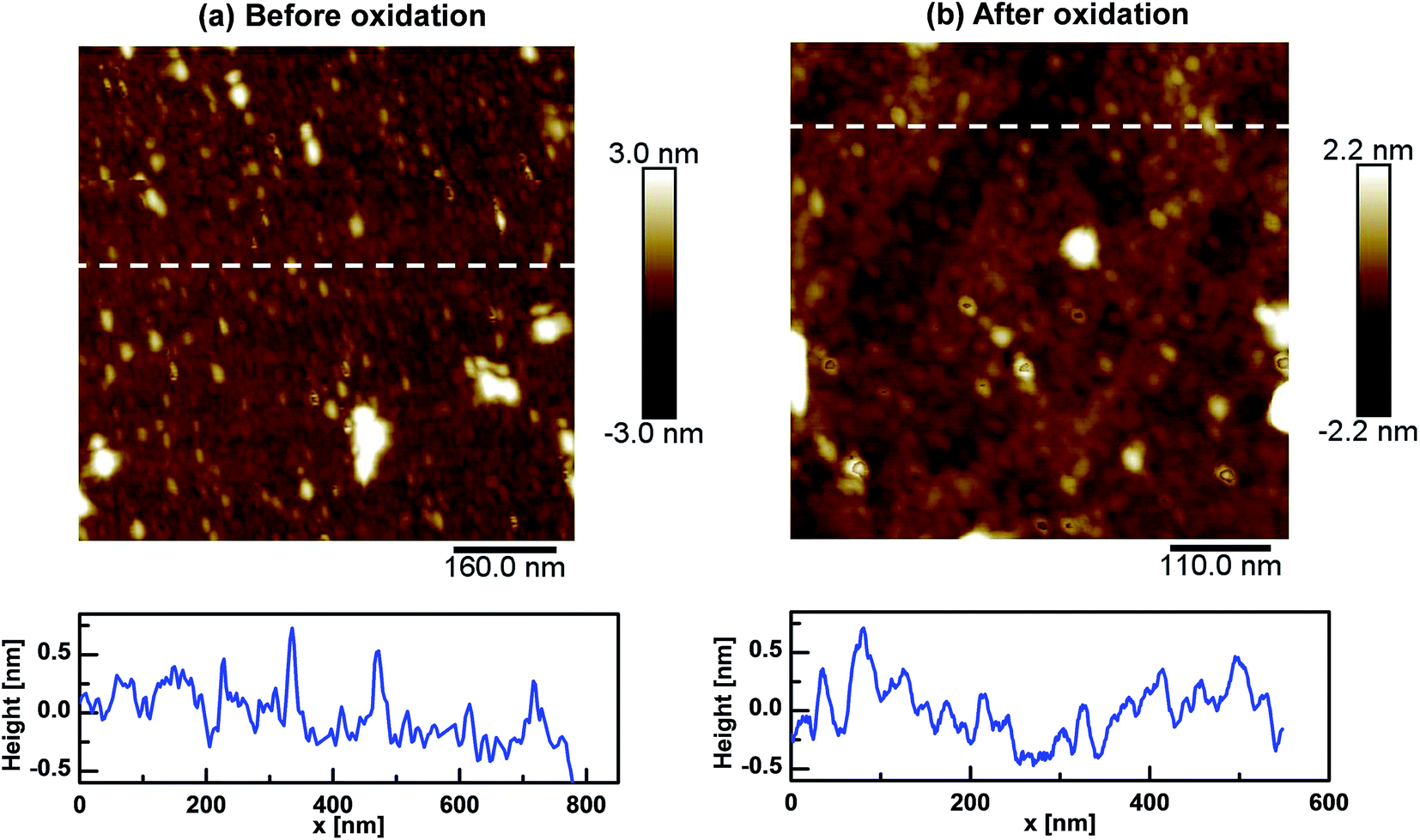 | ||
| Fig. 2 Variation in height across the surface of SLG (a) before and (b) after oxidation obtained using Atomic Force Microscopy (AFM). Representative cross-sections of each height profile are shown below. Oxidation in (b) is performed at T ∼ 678 °C using p(O2) ∼ 2.5 Torr for t ∼ 150 s. AFM scan after oxidation show no pores. The corresponding phase profiles are shown in Fig. 3. | ||
The phase profiles obtained from the tapping mode AFM scans on SLG surfaces before (Fig. 3a) and after (Fig. 3b) oxidation show significant differences. Oxidation results in domains with phase values ∼3–4° higher compared to its surroundings. Similar phase differences have recently been reported during reduction of graphene oxide (GO) between GO and reduced GO (rGO) domains.49 In analogy, we attribute the domains with higher and lower phases as oxidized SLG (O-SLG) and pristine SLG domains. The O-SLG domains are hydrophilic compared to the SLG domains and have higher presence of hydroxyl functionalities that increases tip–surface interaction and hence the phase values during AFM scan in those regions.48,50 Analysis of the phase profile suggests oxidation in ∼30% (obtained by analyzing Fig. 3b using WSXM software51) of the scanned areas. Oxidation also occurred in domains impartial to the regions that had higher transfer residues at the beginning of oxidation (Fig. S3 of ESI†). This potentially suggests nucleation of oxidation at random spots in the SLG that increased in areas over time in a correlated manner; i.e. once oxidation started at a random spot in the SLG, oxidation at nearby spots were more likely that resulted in O-SLG domains of different sizes.
 | ||
| Fig. 3 Variation in the phase of AFM tip while scanning across the surface of SLG (a) before and (b) after pore-free oxidation. Representative cross-sections of each phase profile are shown below. Oxidized (O-SLG) domains and non-oxidized (SLG) regions are marked in (b). Presence of O-SLG domains in the post-oxidation data suggests that the oxidation initiated at random spots and then proceeded in a correlated manner. | ||
Similar to the phase profiles obtained from AFM scan, the O-SLG domains also show noticeable contrast during SEM imaging after SLG oxidation (Fig. 4 and S5 of ESI† contains a larger scale version). Here, SEM was performed using a low (∼1 kV) acceleration voltage to reduce overall charging and hence to increase the contrast. The darker regions in the SEM image indicate lightly charged areas, as expected for the non-conductive O-SLG domains; these areas correspond very well with those having higher phases in the AFM scan (note that SEM performed at a higher acceleration voltage charged the O-SLG domains and removed the contrast between the O-SLG and SLG regions). All these suggest that the oxidation induced metal–insulator transition in the O-SLG areas in a manner which is far beyond O2 adsorption.
 | ||
| Fig. 4 Comparison of (a) AFM phase profile and (b) SEM image (performed using ∼1 kV acceleration voltage) taken at the surface of a micro-pillar, on which SLG is oxidized at T ∼ 653 °C using p(O2) ∼ 2.5 Torr for t ∼ 120 s. The oxidized domains (O-SLG; having higher phases in the AFM scan) appear darker in the SEM image compared to the non-oxidized areas. This suggests O-SLG domains have lower conductivity. | ||
Raman spectroscopy has historically played a powerful role in structural characterization of graphitic materials52 and is used here in ex situ and in situ forms to analyze SLG oxidation. Fig. 5 plots ex situ Raman spectra taken using λ = 514 nm CW laser (power ∼ 1 mW, spot size ∼ 1 μm) before and after SLG oxidation. The post-oxidation Raman spectrum was collected from an area which is larger than the O-SLG domains (shown in Fig. 2b and 3b) and, therefore, had contributions from both the O-SLG and the SLG regions. (Wavelength and temperature dependent Raman spectra collected from SLG before oxidation are presented in Fig. S6 of ESI.† The presented data covers a wider range of temperature compared to that available in graphene literature.53–55) Oxidation incurred distinct blue-shifts (i.e. towards higher frequencies) in the graphitic G-band frequency (ωG: from ∼1588 to ∼1595 cm−1) and the second-order 2D-band frequency (ω2D: from ∼2691 to ∼2705 cm−1) and also reduced the 2D/G peak ratios from ∼1.6 to ∼1.24. Oxidation also increased the magnitude of defect-related D- and D′-bands with associated increase in peak frequencies (ωD: from ∼1353 to 1358 cm−1; ωD′: from ∼1626 to ∼1630 cm−1) and peak ratios (from ∼0.1 to ∼0.86 for the D/G ratio; from ∼2 to ∼3.73 for the D/D′ ratio). It also changed widths of G-band peak from ∼16.1 cm−1 to ∼23.5 cm−1, D′-band peak from ∼20.1 cm−1 to 11.9 cm−1, D-band peak from ∼33.5 cm−1 to 30.5 cm−1 and 2D-band peak from ∼36 cm−1 to ∼47.8 cm−1. Most of these are typically observed during SLG oxidation in various manners.18,19,21,22,34,36 (The in situ Raman data, however, shows a different trend, as discussed later.) Note that the 2D peak, which disappears after complete oxidation of SLG18,19,21,22,36 and is generally absent for GO,56–60 remained in the post-oxidation Raman spectrum due to partial coverage of scanned areas by the O-SLG domains. The remaining Raman bands (the D + D′ band, which appeared at ∼2951 cm−1 after oxidation and the G*-band, which showed a frequency shift from ∼2455 to ∼2471 cm−1) were weak in intensity compared to the others and hence omitted from additional analysis.
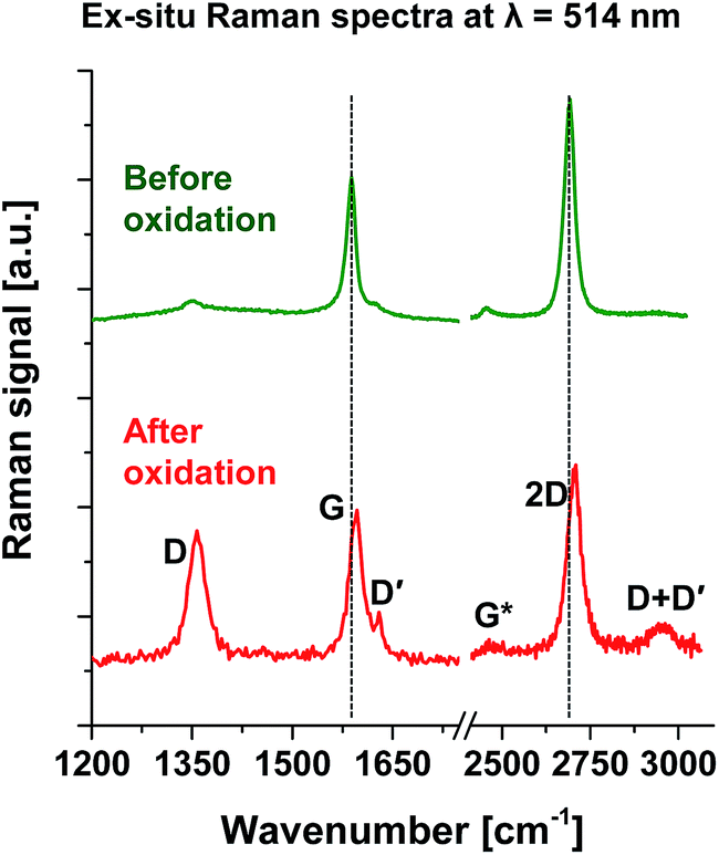 | ||
| Fig. 5 Ex situ Raman spectra taken at λ = 514 nm from SLG before and after oxidation. The post-oxidation Raman spectrum was collected from the oxidized area presented in Fig. 2b and 3b. Representative Raman-band peaks (D-, G-, D′-, G*-, 2D- and D + D′-band peaks) are marked for the post-oxidation spectrum. The horizontal dotted lines represent the peak frequency of the G- and 2D-bands before oxidation suggesting a blue shift (increase in frequency) of all the Raman-band peaks. The defect-related Raman bands (i.e. the D-, D′- and D + D′-bands) are more prominent in the post-oxidation Raman spectrum. | ||
The observation of defect-related Raman peaks before oxidation is possibly related to the defects present at the edges of the SLG patches (see Fig. S2 of ESI†) after the incomplete SLG transfer to micro-pillars. These peaks become prominent after oxidation with a D/G peak ratio of ∼0.86. This value is lower than that observed for oxidized SLG in literature,18,21,22,52 as the post-oxidation Raman spectrum (taken with spot size larger than the size of the O-SLG domains) had contributions from the oxidized and un-oxidized regions. The D/D′ peak ratio of ∼3.73 obtained after oxidation, on the other hand, does not depend on the fraction of O-SLG domains covering the Raman scanned area, as it is a ratio between the Raman signals coming only from the defective (oxidized) regions of SLG. Our recent theoretical analysis61,62 also calculated a similar D/D′ peak ratio for the SLG functionalized with molecular O2 – suggesting the presence of small (not leading to visible pores during AFM scan), broad types of vacancies in the O-SLG domains.
In situ Raman data collected during SLG oxidation provided a unique opportunity to understand the nature of oxidation over time. Fig. 6a plots the temporal evolution of the Raman spectrum in the D- and G-band regions from the SLG-covered micro-pillar during oxidation at p(O2) ∼ 2.5 Torr, T ∼ 678 °C. At this high temperature, the Raman-bands were broadened such that the G-band overshadowed the D′-band. An estimation of the evolution in D′-band was, therefore, impossible. The intensities of the D- and G-band peaks were extracted from the in situ data to calculate the D/G peak ratio, which is plotted against t in Fig. 6b. The D/G peak ratio increased with oxidation up to ∼0.8 and then slightly dropped down. In literature, significant decrease in the D/G ratio was observed during defect formation in SLG using energetic oxygen,21,22,34 hydrogen21,63 or argon52,64 species and was attributed to the formation of sp3-hybridized defects and vacancies before and after the inflection point, respectively. To confirm whether this applies to the samples studied here would require a thorough investigation of the atomic structure of the oxidized regions, which is beyond the scope of this article. Note that due to differences in the spot sizes for the ex situ (∼1 μm) and in situ (∼7 μm) Raman analysis and also due to partial coverage of scanned areas by the O-SLG domains, the in situ D/G peak ratio obtained at the end of oxidation (∼0.7 in Fig. 6b) is different from the ex situ value (∼0.86 in Fig. 5). The incomplete oxidation of SLG on the micro-pillars also explains the observation of a lower maximum for the D/G peak ratio in Fig. 6b compared to that (∼100/EL−4 ∼ 3.4; where EL is the laser energy) in literature.21,22,34,52,64 Results from a controlled experiment performed by exposing SLG to O2 at a lower pressure of oxygen, p(O2) ∼ 1.25 mTorr and at a lower temperature T ∼ 378 °C showed negligible change in the D/G peak ratio (Fig. 6c and d). A mild O2 exposure, therefore, is not conducive to SLG oxidation or defect formation. AFM scans on this mildly exposed SLG also showed no signs of phase change.
 | ||
| Fig. 6 Cascade plots of time dependent D-band and G-band Raman spectra during oxidation of SLG (a) at p(O2) ∼ 2.5 Torr, T ∼ 678 °C and (c) at p(O2) ∼ 1.25 mTorr, T ∼ 378 °C. Time evolution of the D/G peak ratios from analysis of the in situ Raman spectra in (a) and (c) are shown in (b) and (d), respectively. The lines in (b) and (d) are guide to the eye only. | ||
Irrespective of the level of oxidation, ωG exhibited a continuous blue-shift, while ω2D exhibited an initial blue-shift, followed by an eventual red-shift over time (Fig. 7). As blue- and red-shifts in ω2D originates from p- and n-doping, respectively,65 the initial blue-shift in ω2D is attributed to p-doping of SLG via O2 adsorption. The subsequent red-shift in ω2D is attributed to the n-doping of SLG due to desorption of hydroxyl (–OH) groups during high temperature processing. The time at which the effect from –OH desorption was visible (i.e. at ∼40 s in Fig. 7a and at ∼10 s in Fig. 7b) decreased with the decrease in p(O2). In order to confirm that the observed initial p-doping of the SLG was indeed due to O2 adsorption, SLG was annealed at ∼300 °C in vacuum (0.1 mTorr). This resulted in a monotonous blue-shift in ωG and only a red-shift in ω2D (Fig. S7 of ESI†) due to –OH desorption. Note that although the in situ Raman data suggested an overall red-shift in ω2D at the end of oxidation, the ex situ Raman data collected after oxidation exhibited a blue-shift in ω2D compared to the pre-oxidized values (Fig. 5). This was due to re-adsorption of –OH groups (more due to the hydrophilic nature of O-SLG) once the sample was exposed to ambient conditions for the ex situ Raman scan.
 | ||
| Fig. 7 Time evolution of the G-, 2D-band peak frequencies (ωG and ω2D, respectively) with respect to their pre-oxidized values obtained from the analysis of in situ Raman measurements during oxidation of SLG (a) at p(O2) ∼ 2.5 Torr, T ∼ 678 °C and (b) at p(O2) ∼ 1.25 mTorr, T ∼ 378 °C. The lines are guide to the eye only. | ||
The effect of temperature on the kinetics of SLG oxidation is presented next. The time dependence of the D/G ratio at different temperatures with a fixed p(O2) ∼ 2.5 Torr is shown in Fig. 8a. For T < 600 °C, the D/G ratio continuously increased over time. At higher temperatures, the D/G ratio reached a maximum (which happened at smaller t for higher T) and then dropped down. This inflection in the D/G ratio is possibly due to the formation of different types of defects before (sp3-hybridized) and after (vacancies) the inflection point.21 The oxidation at a reduced oxygen pressures of p(O2) ∼ 1.25 mTorr yielded slower kinetics and did not show significant increase in the D/G ratio for T < 600 °C (Fig. 8b). At higher temperatures, however, the D/G ratio increased over time and showed an inflection point around t ∼ 170 s at T ∼ 740 °C. This occurrence of the inflection point at a longer time compared to that in Fig. 8a suggests differences in the degrees of oxidation at different p(O2).
 | ||
| Fig. 8 Time dependence of the D/G ratios measured at different T for (a) p(O2) ∼ 2.5 Torr and (b) p(O2) ∼ 1.25 mTorr. The lines correspond to fits using eqn (1). The fitting parameters for a few temperatures are listed in the tables below. The parameters at lower temperatures are not unique; hence those fitted lines are not shown and corresponding parameters are not tabulated. | ||
For an analysis of the defect density in SLG, the phenomenological model64 relating the D/G ratio with lattice defects in graphene is considered; hence, the following expression is used to analyze the variation in the D/G peak ratio:
 | (1) |
| D/G|t∼0 = D/G|0 + FGπPT2t2[CSrS2 + CA(rA2 − rS2)]. | (2) |
To derive eqn (2), LD is approximated as 1/(PTt), where t is the oxidation time and PT is a proportionality constant that varies with oxidation temperature and p(O2). The quadratic time dependence of (D/G|t∼0 − D/G|0) in eqn (2) is a consequence of the LD ∼ 1/t assumption. Oxidation performed at a reduced p(O2) has a slower time dynamics and therefore allows analysis of the initial phases of oxidation for justification of the LD ∼ 1/t assumption. Fig. S8 of ESI† signifies a clear quadratic time dependence for (D/G|t∼0 − D/G|0) at p(O2) ∼ 1.25 mTorr and at T ∼ 660–740 °C, therefore, justifies the LD ∼ 1/t assumption used in eqn (2). A fit of all the oxidation data using eqn (1) with LD replaced with 1/(PTt) allows extraction of the variations in PT and FG with temperature and p(O2). The extracted values are tabulated at the bottom parts of Fig. 8. An increase in PT with the increase in T and p(O2) corroborates with the expected increase in the oxidation rate at these conditions. The values of FG in Fig. 8a suggest O-SLG domains occupying ∼10–15% (=FG × 100%) of the total scanned area by in situ Raman spectroscopy, which is less than the ∼30% coverage obtained from ex situ Raman scan in Fig. 3b for a similar oxidation condition. The larger spot size (∼7 μm for the full-width half maximum) and higher power (>1 W) of the incident laser beam used for in situ Raman spectroscopy can account for this difference. These conditions induced acquisition of Raman signals from a wider area of the micro-pillar, therefore, reduced the contribution from the O-SLG domains in the in situ Raman data. A higher oxidation temperature increased the coverage of O-SLG domains and hence FG (Fig. 8b). The parameters extracted in Fig. 8 will allow control of graphene oxidation at the conditions for which eqn (1) is fitted for. A finer control on oxidation at any given time, temperature and pressure will require fitting of the measured D/G ratio with eqn (1) for a wider range of oxidation conditions, which will be a topic of future study.
The in situ Raman data presented in Fig. 8 additionally allows calculation of the reaction energy (ER) for SLG oxidation and hence to obtain mechanistic insight into the oxidation process. To calculate ER, the D/G peak ratio at different temperatures was determined at a fixed time (∼100 s). The difference between D/G|t=100 s and D/G|t=0 (≡Δ(D/G)) is plotted as a function of 1/kBT (Fig. 9), where kB is the Boltzmann's constant. ER was then extracted from the slope of the Δ(D/G) vs. 1/kBT curves; ER varies from ∼0.8 ± 0.17 eV to ∼1.11 ± 0.21 eV for the two oxidation conditions (i.e., p(O2) ∼ 2.5 Torr and 1.25 mTorr, respectively) studied here. These values have potential contributions from defect formation in the SLG lattice and from reactions of oxygen species with the SLG and its defects. In fact, the ER values are similar to the energies obtained for reactions of singlet O2 with carbon atoms in a graphitic lattice,5,66 which suggests possible conversion of O2 to an active oxygen species like singlet O2 during the high-power laser exposure. The other possible sources of oxidation from O2 and ozone are ruled out, as they react with graphitic carbons at temperatures much higher67 and lower18,22,33,68 than the values used here. To understand more on the active oxygen species for the observed pore-free oxidation, a separate set of experiments were carried out where SLG (transferred on to SiO2 substrates) was exposed directly to O2 at temperatures up to 650 °C and at p(O2) ∼ 5 Torr in an environmental microscope stage (Linkam Scientific). This O2 exposure did not yield any insignificant increase in the D/G peak ratio (Fig. S9 of ESI†). On the other hand, SLG exposure to ozone at temperatures < 200 °C and at pressures < 30 Torr yielded high D/G peak ratio with large pores (Fig. S10 of ESI†) potentially near the grain boundaries of SLG.21
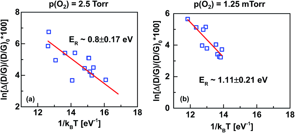 | ||
| Fig. 9 Arrhenius plots of the percentage change in the D/G ratios, Δ(D/G), over their pre-oxidized values, (D/G)|0, as a function of 1/kBT for (a) p(O2) ∼ 2.5 Torr and (b) p(O2) ∼ 1.25 mTorr. The extracted reaction energies (ER) of SLG oxidation at different p(O2) are noted in respective figures. | ||
Photo-activation of O2 from the ground triplet to the excited singlet states is well-known in literature.69 This singlet state of O2 is presumably the active oxygen species for the laser induced oxidation studied here. In addition to the photo-activated singlet O2, however, temperature is also responsible for the observed SLG oxidation. To confirm this, we exposed the SLGs placed on planar SiO2/Si substrates to photo-activated O2 generated with a laser power up to ∼4 W. The temperatures of the exposed areas increased up to 200–300 °C, however, SLG did not show any sign of oxidation. (This last observation further rules out the possibility of photo-conversion of O2 to ozone, as ozone normally oxidizes SLG at temperatures < 200 °C.18,22,33,68) All these suggest that the photo-activated oxygen species (possibly singlets of O2) results in pore-free oxidation of SLG via a thermal process with the reaction energies shown in Fig. 9.
Conclusions
We obtained pore-free oxidation of single-layer graphene by exposing the material to photo-excited oxygen species. Surface analysis using atomic force microscopy suggested that the oxidized areas were randomly distributed in nanoscale domains across the graphene layer. The mechanism of oxidation was also studied using in situ Raman spectroscopy to monitor the time evolution of different Raman peaks. The origin of in situ peak shifts (blue-shift for G-band and red shift for 2D-band) was attributed to desorption of –OH groups during the high temperature oxidation process. The re-adsorption of these –OH groups in ambient condition resulted in blue-shifts for both of the Raman G- and 2D-band peaks, as observed during ex situ Raman spectroscopy. Empirical analysis of the time evolution of oxygenated defects suggested quadratic time dependence for defect density at lower levels of oxidation and a systematic variation of the proportionality constant with temperature and oxidation pressure at different times. The analysis of the in situ Raman data at various conditions also enabled extraction of fundamental parameters such as reaction energy for the metal–insulator transition in single-layer graphene and identified photo-excited singlet O2 as the active oxygen species. In comparison with the oxygen species such as oxygen plasma, ozone and high pressure O2 explored in literature for graphene oxidation, the singlet O2 at ≤2.5 Torr pressure reacted with graphene in a milder way and induced oxidation of graphene in a controlled and pore-free manner. Future exploration of such controlled chemical modification of graphene will enable defect engineering of graphene at different size scales and hence will greatly expand the use of graphene in many envisaged applications.Acknowledgements
Financial support from National Research Council (Contract Number: FA9550-12-D-0001) and Air Force Office of Scientific Research (Program Manager: Dr Charles Lee; Task Number: 3002MR12P/14RX03COR) are acknowledged for preparation of this manuscript.References
- A. K. Geim and K. S. Novoselov, Nat. Mater., 2007, 6, 183–191 CrossRef CAS PubMed.
- K. S. Novoselov, A. K. Geim, S. V. Morozov, D. Jiang, M. I. Katsnelson, I. V. Grigorieva, S. V. Dubonos and A. A. Firsov, Nature, 2005, 438, 197–200 CrossRef CAS PubMed.
- V. Georgakilas, M. Otyepka, A. B. Bourlinos, V. Chandra, N. Kim, K. C. Kemp, P. Hobza, R. Zboril and K. S. Kim, Chem. Rev., 2012, 112, 6156–6214 CrossRef CAS PubMed.
- T. Kuila, S. Bose, A. K. Mishra, P. Khanra, N. H. Kim and J. H. Lee, Prog. Mater. Sci., 2012, 57, 1061–1105 CrossRef CAS.
- D. W. Boukhvalov and M. I. Katsnelson, J. Phys.: Condens. Matter, 2009, 21, 344205 CrossRef CAS PubMed.
- L. Dai, Acc. Chem. Res., 2013, 46, 31–42 CrossRef CAS PubMed.
- J. M. Englert, C. Dotzer, G. Yang, M. Schmid, C. Papp, J. M. Gottfried, H.-P. Steinrueck, E. Spiecker, F. Hauke and A. Hirsch, Nat. Chem., 2011, 3, 279–286 CrossRef CAS PubMed.
- J. E. Johns and M. C. Hersam, Acc. Chem. Res., 2013, 46, 77–86 CrossRef CAS PubMed.
- A. Criado, M. Melchionna, S. Marchesan and M. Prato, Angew. Chem., Int. Ed., 2015, 54, 10734–10750 CrossRef CAS PubMed.
- F. M. Koehler, A. Jacobsen, K. Ensslin, C. Stampfer and W. J. Stark, Small, 2010, 6, 1125–1130 CrossRef CAS PubMed.
- S. Eigler and A. Hirsch, Angew. Chem., Int. Ed., 2014, 53, 7720–7738 CrossRef CAS PubMed.
- D. A. C. Brownson, D. K. Kampouris and C. E. Banks, Chem. Soc. Rev., 2012, 41, 6944–6976 RSC.
- D. A. C. Brownson, A. C. Lacombe, M. Gomez-Mingot and C. E. Banks, RSC Adv., 2012, 2, 665–668 RSC.
- W. Deng, X. Ji, M. Gomez-Mingot, F. Lu, Q. Chen and C. E. Banks, Chem. Commun., 2012, 48, 2770–2772 RSC.
- R. Lv, Q. Li, A. R. Botello-Mendez, T. Hayashi, B. Wang, A. Berkdemir, Q. Hao, A. L. Elias, R. Cruz-Silva, H. R. Gutierrez, Y. A. Kim, H. Muramatsu, J. Zhu, M. Endo, H. Terrones, J.-C. Charlier, M. Pan and M. Terrones, Sci. Rep., 2012, 2, 586 Search PubMed.
- W. Lee, S. Suzuki and M. Miyayama, Electrochim. Acta, 2014, 142, 240–246 CrossRef CAS.
- L. Qu, Y. Liu, J.-B. Baek and L. Dai, ACS Nano, 2010, 4, 1321–1326 CrossRef CAS PubMed.
- S. Huh, J. Park, Y. S. Kim, K. S. Kim, B. H. Hong and J.-M. Nam, ACS Nano, 2011, 5, 9799–9806 CrossRef CAS PubMed.
- L. Liu, S. Ryu, M. R. Tomasik, E. Stolyarova, N. Jung, M. S. Hybertsen, M. L. Steigerwald, L. E. Brus and G. W. Flynn, Nano Lett., 2008, 8, 1965–1970 CrossRef CAS PubMed.
- S. Ryu, L. Liu, S. Berciaud, Y.-J. Yu, H. Liu, P. Kim, G. W. Flynn and L. E. Brus, Nano Lett., 2010, 10, 4944–4951 CrossRef CAS PubMed.
- M. Seifert, J. E. B. Vargas, M. Bobinger, M. Sachsenhauser, A. W. Cummings, S. Roche and J. A. Garrido, 2D Materials, 2015, 2, 024008 CrossRef.
- J. Yuan, L.-P. Ma, S. Pei, J. Du, Y. Su, W. Ren and H.-M. Cheng, ACS Nano, 2013, 7, 4233–4241 CrossRef CAS PubMed.
- Z. Yang, Z. Yao, G. Li, G. Fang, H. Nie, Z. Liu, X. Zhou, X. A. Chen and S. Huang, ACS Nano, 2012, 6, 205–211 CrossRef CAS PubMed.
- F. Shahzad, S. Yu, P. Kumar, J.-W. Lee, Y.-H. Kim, S. M. Hong and C. M. Koo, Compos. Struct., 2015, 133, 1267–1275 CrossRef.
- R. K. Shervedani and A. Amini, Carbon, 2015, 93, 762–773 CrossRef CAS.
- P. A. Denis, Chem. Phys. Lett., 2010, 492, 251–257 CrossRef CAS.
- H. Gao, Z. Liu, L. Song, W. Guo, W. Gao, L. Ci, A. Rao, W. Quan, R. Vajtai and P. M. Ajayan, Nanotechnology, 2012, 23, 275605 CrossRef PubMed.
- S. Kundu, R. M. Yadav, T. N. Narayanan, M. V. Shelke, R. Vajtai, P. M. Ajayan and V. K. Pillai, Nanoscale, 2015, 7, 11515–11519 RSC.
- D. Geng, Y. Chen, Y. Chen, Y. Li, R. Li, X. Sun, S. Ye and S. Knights, Energy Environ. Sci., 2011, 4, 760–764 CAS.
- Y. Li, Y. Zhao, H. Cheng, Y. Hu, G. Shi, L. Dai and L. Qu, J. Am. Chem. Soc., 2012, 134, 15–18 CrossRef CAS PubMed.
- Z.-S. Wu, S. Yang, Y. Sun, K. Parvez, X. Feng and K. Muellen, J. Am. Chem. Soc., 2012, 134, 9082–9085 CrossRef CAS PubMed.
- R. Cruz-Silva, A. Morelos-Gomez, S. Vega-Diaz, F. Tristan-Lopez, A. L. Elias, N. Perea-Lopez, H. Muramatsu, T. Hayashi, K. Fujisawa, Y. A. Kim, M. Endo and M. Terrones, ACS Nano, 2013, 7, 2192–2204 CrossRef CAS PubMed.
- N. Leconte, J. Moser, P. Ordejon, H. Tao, A. Lherbier, A. Bachtold, F. Alsina, C. M. Sotomayor Torres, J.-C. Charlier and S. Roche, ACS Nano, 2010, 4, 4033–4038 CrossRef CAS PubMed.
- I. Childres, L. A. Jauregui, J. Tian and Y. P. Chen, New J. Phys., 2011, 13, 025008 CrossRef.
- D. C. Kim, D.-Y. Jeon, H.-J. Chung, Y. Woo, J. K. Shin and S. Seo, Nanotechnology, 2009, 20, 375703 CrossRef PubMed.
- A. Zandiatashbar, G.-H. Lee, S. J. An, S. Lee, N. Mathew, M. Terrones, T. Hayashi, C. R. Picu, J. Hone and N. Koratkar, Nat. Commun., 2014, 5, 3186 Search PubMed.
- M. Y. Han, B. Oezyilmaz, Y. Zhang and P. Kim, Phys. Rev. Lett., 2007, 98, 206805 CrossRef PubMed.
- C. Berger, Z. Song, X. Li, X. Wu, N. Brown, C. Naud, D. Mayou, T. Li, J. Hass, A. N. Marchenkov, E. H. Conrad, P. N. First and W. A. de Heer, Science, 2006, 312, 1191–1196 CrossRef CAS PubMed.
- J. Aumanen, A. Johansson, J. Koivistoinen, P. Myllyperkio and M. Pettersson, Nanoscale, 2015, 7, 2851–2855 RSC.
- Z. Xu and K. Xue, Nanotechnology, 2009, 21, 045704 CrossRef PubMed.
- J.-A. Yan and M. Y. Chou, Phys. Rev. B: Condens. Matter Mater. Phys., 2010, 82, 125403 CrossRef.
- R. Rao, D. Liptak, T. Cherukuri, B. I. Yakobson and B. Maruyama, Nat. Mater., 2012, 11, 213–216 CrossRef CAS PubMed.
- P. Nikolaev, D. Hooper, N. Perea-Lopez, M. Terrones and B. Maruyama, ACS Nano, 2014, 8, 10214–10222 CrossRef CAS PubMed.
- R. Rao, A. E. Islam, N. Pierce, P. Nikolaev and B. Maruyama, Carbon, 2015, 95, 287–291 CrossRef CAS.
- R. Rao, N. Pierce, D. Liptak, D. Hooper, G. Sargent, S. L. Semiatin, S. Curtarolo, A. R. Harutyunyan and B. Maruyama, ACS Nano, 2013, 7, 1100–1107 CrossRef CAS PubMed.
- Y. Y. Wang, Z. H. Ni, Z. X. Shen, H. M. Wang and Y. H. Wu, Appl. Phys. Lett., 2008, 92, 043121 CrossRef.
- A. Eckmann, A. Felten, A. Mishchenko, L. Britnell, R. Krupke, K. S. Novoselov and C. Casiraghi, Nano Lett., 2012, 12, 3925–3930 CrossRef CAS PubMed.
- J. I. Paredes, A. Martinez-Alonso and J. M. D. Tascon, Langmuir, 2003, 19, 7665–7668 CrossRef CAS.
- J. I. Paredes, S. Villar-Rodil, P. Solis-Fernandez, A. Martinez-Alonso and J. M. D. Tascon, Langmuir, 2009, 25, 5957–5968 CrossRef CAS PubMed.
- J. I. Paredes, A. Martinez-Alonso and J. M. D. Tascon, Langmuir, 2002, 18, 4314–4323 CrossRef CAS.
- I. Horcas, R. Fernandez, J. M. Gomez-Rodriguez, J. Colchero, J. Gomez-Herrero and A. M. Baro, Rev. Sci. Instrum., 2007, 78, 013705 CrossRef CAS PubMed.
- L. G. Cancado, A. Jorio, E. H. Martins Ferreira, F. Stavale, C. A. Achete, R. B. Capaz, M. V. O. Moutinho, A. Lombardo, T. S. Kulmala and A. C. Ferrari, Nano Lett., 2011, 11, 3190–3196 CrossRef CAS PubMed.
- M. R. Joya, A. R. Zanatta and J. Barba-Ortega, Mod. Phys. Lett. B, 2013, 27, 1350203 CrossRef.
- I. Calizo, I. Bejenari, M. Rahman, G. Liu and A. A. Balandin, J. Appl. Phys., 2009, 106, 043509 CrossRef.
- I. Calizo, S. Ghosh, W. Bao, F. Miao, C. N. Lau and A. A. Balandin, Solid State Commun., 2009, 149, 1132–1135 CrossRef CAS.
- G. Eda and M. Chhowalla, Adv. Mater., 2010, 22, 2392–2415 CrossRef CAS PubMed.
- C. Gomez-Navarro, R. T. Weitz, A. M. Bittner, M. Scolari, A. Mews, M. Burghard and K. Kern, Nano Lett., 2007, 7, 3499–3503 CrossRef CAS PubMed.
- K. P. Loh, Q. Bao, G. Eda and M. Chhowalla, Nat. Chem., 2010, 2, 1015–1024 CrossRef CAS PubMed.
- S. Stankovich, D. A. Dikin, R. D. Piner, K. A. Kohlhaas, A. Kleinhammes, Y. Jia, Y. Wu, S. T. Nguyen and R. S. Ruoff, Carbon, 2007, 45, 1558–1565 CrossRef CAS.
- D. Yang, A. Velamakanni, G. Bozoklu, S. Park, M. Stoller, R. D. Piner, S. Stankovich, I. Jung, D. A. Field, C. A. Ventrice Jr and R. S. Ruoff, Carbon, 2009, 47, 145–152 CrossRef CAS.
- J. Jiang, R. Pachter, F. Mehmood, A. E. Islam, B. Maruyama and J. J. Boeckl, Carbon, 2015, 90, 53–62 CrossRef CAS.
- J. Jiang, R. Pachter, T. Demeritte, P. C. Ray, A. Islam, B. Maruyama and J. Boeckl, J. Phys. Chem. C, 2016, 120, 5371–5383 CAS.
- Z. Luo, T. Yu, K.-J. Kim, Z. Ni, Y. You, S. Lim, Z. Shen, S. Wang and J. Lin, ACS Nano, 2009, 3, 1781–1788 CrossRef CAS PubMed.
- M. M. Lucchese, F. Stavale, E. H. M. Ferreira, C. Vilani, M. V. O. Moutinho, R. B. Capaz, C. A. Achete and A. Jorio, Carbon, 2010, 48, 1592–1597 CrossRef CAS.
- A. Das, S. Pisana, B. Chakraborty, S. Piscanec, S. K. Saha, U. V. Waghmare, K. S. Novoselov, H. R. Krishnamurthy, A. K. Geim, A. C. Ferrari and A. K. Sood, Nat. Nanotechnol., 2008, 3, 210–215 CrossRef CAS PubMed.
- S. P. Chan, G. Chen, X. G. Gong and Z. F. Liu, Phys. Rev. Lett., 2003, 90, 086403 CrossRef PubMed.
- J. M. Carlsson, F. Hanke, S. Linic and M. Scheffler, Phys. Rev. Lett., 2009, 102, 166104 CrossRef PubMed.
- G. Lee, B. Lee, J. Kim and K. Cho, J. Phys. Chem. C, 2009, 113, 14225–14229 CAS.
- A. A. Krasnovsky Jr, Biochemistry, 2007, 72, 1065–1080 CAS.
Footnote |
| † Electronic supplementary information (ESI) available. See DOI: 10.1039/c6ra05399h |
| This journal is © The Royal Society of Chemistry 2016 |