
Transfer of metallic nanostructures from solid-state substrates
K. Kolářová*a,
R. Krajcara,
P. Ulbrichb and
V. Švorčíka
aDepartment of Solid State Engineering, University of Chemistry and Technology, Prague, Technicka 5, 166 28 Prague, Czech Republic. E-mail: kolarova@vscht.cz
bDepartment of Biochemistry and Microbiology, University of Chemistry and Technology, Prague, Technicka 5, 166 28 Prague, Czech Republic
First published on 18th April 2016
Abstract
A novel technique for transferring dimensionally diverse metallic nanostructures from different kinds of substrates into chitosan foil is described. We were able to obtain nanoparticles of different sizes and shapes incorporated into the surface of a biocompatible polymer with no restrictions on the process used to manufacture the structures supported on the initial substrate. We successfully transferred silver nanowires (NWs) from a nano-patterned polyethyleneterephthalate (PET) foil, and silver nanoparticles (NPs) from a microscope cover glass.
Recently, material engineers have paid considerable attention to preparing nanostructures on the surfaces of solid-state substrates. Various methods have been developed to achieve such products, e.g., lithography,1 use of laser-induced periodic surface structures (LIPSS),2 and many kinds of deposition techniques.3 The interest here has been mainly focused on noble metals, especially silver due to its having the highest electrical and thermal conductivities of all metals. Silver on the nanoscale is widely used for its catalytic and antibacterial properties.4,5 Its interesting optical properties in the visible spectral range have given rise to applications in photonics, optoelectronics and sensing devices.6,7
How surfaces containing nanostructures are utilized is not only determined by the size, shape and material properties of the surface metal, but it also depends on the composition and topography of the substrate underneath.8 The selection of a substrate suitable for a given application is very often limited by the technique available for preparing the final product. Polymers are very promising materials for substrates due to their light weight, chemical stability and easy patterning.
Here we demonstrate a novel technique suitable for transfer of metallic nanostructures of various sizes and shapes from different types of solid-state substrates into chitosan film. We focused both on the transfer of silver nanowires (NWs) with high aspect ratios as well as on silver nanoparticles (NPs) of hemispherical shape to underscore the flexibility of the transfer mechanism.
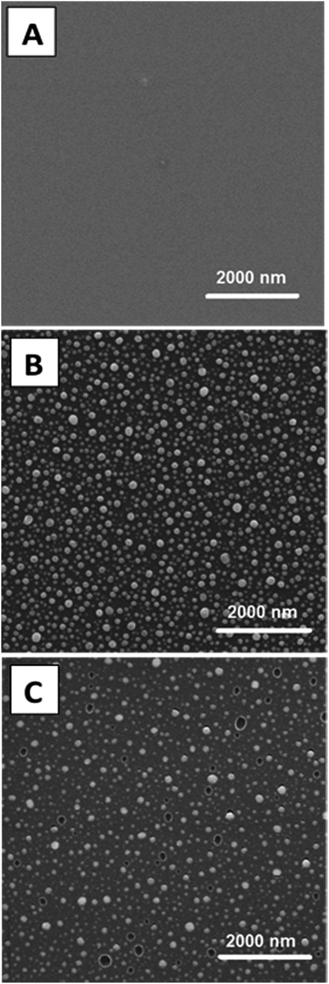
We also applied two different methods to prepare the initial nanostructures. At first we prepared silver NWs on a polyethyleneterephthalate (PET) substrate. A PET foil (biaxially oriented foils, Goodfellow LtD., thickness 50 μm) was modified with a KrF excimer pulse laser (Lambda Physik Compex Pro 50, λ = 248 nm, frequency of 10 Hz) to prepare a ripple-like pattern9 (Fig. 1A). The modification was performed with 6000 laser pulses and a fluence of 7 mJ cm−2.10 The irradiated area was 5 × 10 mm2. The periodicity of the pattern (Λ = 230 nm) and its depth (d = 35 nm) were established using atomic force microscopy (AFM). A surface-modified foil was used as a template for vacuum evaporation of silver under a 70° glancing angle of incidence (Fig. 1B).11 This glancing angle geometry led to the crystallization of silver predominantly on the ridges of PET ripples, which provided for well-separated NWs. The approximate average thickness of the silver NWs (20 nm) was established by scratch tests on a glass substrate coated simultaneously with the PET template under the same conditions. The average width of the prepared nanowires (approximately 100 nm) was measured using scanning electron microscopy (SEM) and atomic force microscopy (AFM). We assumed that the NWs extended over the entire length of the sample (10 mm), which was supported by measurements of the electrical resistance in the longitudinal and transverse directions.10,12,13 NPs were prepared by sputtering (Sputter Coater Bal-Tec SCD 050, with a sputtering time of 140 s, and direct current of 20 mA) of a thin film of silver on a microscope cover glass (borosilicate glass 24 × 24 mm2, Menzel) followed by its thermal annealing.14 The film thickness (10 nm) was established by scratch tests using AFM. Under an elevated temperature (300 °C), individual island-like structures (NPs) were formed by a solid-state dewetting process. Dewetting is driven by surface/interface energy minimization.15 This phenomenon is controlled by the interplay between thermodynamics and kinetics. A continuous coverage of substrate at room temperature is a metastable state, because the surface energy of the metal is greater than that of the substrate material. Thermodynamics drives such a system toward a geometry where contact between the metal and the substrate is minimized. However, the atoms lack sufficient kinetic energy during the deposition process. Heating such a metastable film drives it toward the equilibrium state, where the metal agglomerates into nanostructures at temperatures well below the melting point of the metal.16 Dewetting therefore leads to evolution of island-like structures (silver NPs). In our case, the silver nano-islands were formed with a wide particle size distribution from tens to hundreds of nanometers (Fig. 4B). Finally, we obtained two completely different types of silver nanostructures on different types of substrates, prepared by different techniques. Samples containing NWs and NPs were placed into the silicone plates, which were filled with a 0.5% solution of chitosan (highly viscous chitosan from crab shells, SIGMA-ALDRICH) in diluted 2.0% acetic acid17 (Fig. 1C). Silicone plates were placed into a dryer and annealed under 60 °C conditions to desiccate them of surplus water. After a few hours, the solid chitosan film in contact with the surface of the initial substrate was prepared. Chitosan was separated from the initial substrate by simple peeling using tweezers (Fig. 1D). During the peeling, the metallic nanostructures embedded in the chitosan were transferred from the initial (PET or glass) substrate (Fig. 1E). Chitosan is a linear linked polysaccharide. Due to its many primary amine groups, chitosan can bind and hence filter and detect heavy metal ions18 and also shows other useful properties including biocompatibility, biodegradability and antibacterial activity. These properties allow chitosan to be used in tissue engineering, drug delivery systems, membrane systems, biosensors and other specific biofabrications. Chitosan chelates many transition metal ions.19 It is a very promising chelating agent once the proper working conditions are determined (e.g., pH, concentration).20 This specific interaction between chitosan molecules and metallic particles enables chitosan to be used as a stabilizing agent to prevent aggregation during wet synthesis. In many applications, chitosan serves as a medium for entrapment of nanoparticles.21 Stronger bonding between silver and chitosan in comparison to silver and the original template was crucial for the success of our peeling process. Moreover, the peeling process is applicable for more than only silver NWs and NPs on PET and glass templates, respectively, but it should be performed every time when the bonding between particles and chitosan is stronger than the bonding between particles and original substrate. In this way, metallic nanoparticles of different chemical compositions (even different sizes and shapes) can be transferred from various types of substrates (glass, other polymers, silicon, etc.). The great advantage of the peeling method is the possibility to obtain metallic nanostructures incorporated into chitosan foil with no restrictions on the original process used to manufacture the particles. The method is simple, inexpensive, and environmentally friendly with no need for special equipment. The peeling process also does not exhibit any limitations with regards to the area of substrate undergoing the transfer. The transfer of the nanostructures can be detected by the naked eye. The PET and glass substrates with silver coatings that we used displayed a specific color, and both became optically transparent after the peeling was done. Optical properties of the samples were studied by performing UV-Vis spectroscopy experiments before and after the peeling process (Fig. 2). The nanowires were studied by shining linearly polarized light perpendicular to the major axis of the wire (Fig. 2A). A shift of the plasmon from 600 nm to 565 nm after peeling could be attributed to different refractive indexes of the PET (n = 1.64) and chitosan (n = 1.55) substrates, because a decrease of the refractive index of a surrounding medium has been shown to cause shifts of SPR bands towards smaller wavelengths.22 We also observed a spatial effect altering the plasmonic properties, in particular in the case of hemispherical nanoparticles, as shown in Fig. 2B. In this case, there was a slight blue shift of the absorbance peak after peeling, even though the refractive index of glass (n = 1.52) is smaller than that of chitosan. The silver NPs on the glass substrate could be described as particles supported on a dielectric substrate, but in the case of chitosan, the nanoparticles were observed to be more or less embedded into the chitosan matrix. Embedding medium or adsorbates have been found to induce shifts of SPR and peak broadening,23 which we also clearly observed, as shown in Fig. 2B. The higher overall absorbance of NPs in chitosan than with the glass substrate may have been caused by light scattering from relatively rough chitosan surface. The plasmon peak at 355 nm on the glass was attributed to the quadrupole resonance mode24 and its occurrence also led to a decrease in the intensity of the dipole plasmon. Schmidl et al. studied optical properties of silver NPs prepared by annealing of a thin film on a glass substrate (similar to the approach we used). They deposited different dielectric cover films on the samples (silver NPs on glass), which led to peak broadening, spectral shift and disappearance of the quadrupole plasmon mode, as we also observed, as shown in Fig. 2B. The transfer of metallic nanostructures by peeling was successful because there were no (or at least negligible) traces of residual metal on the PET or glass surface after the process. (Peeled PET and peeled glass did not yield curves exhibiting any optical features indicative of the presence of silver.) Silver nanostructures and their transport were observed by using SEM (VEGA 3 LMU, TESCAN). Fig. 3A shows the image of an uncoated laser-patterned PET (corresponds with Fig. 1A), which was used as a template for deposition of silver. Prepared NWs can be seen in Fig. 3B. The average width of the wires was observed to be approximately half of the dimension of the period (Λ = 230 nm), and this observation was consistent with the geometry of the evaporation process. Atoms of evaporated silver were found to occupy positions predominantly on the ridges of the periodic linear polymers, so that the NWs exhibited an irregular cross-section and were located on the outer side of the ridges (see Fig. 1B). Fig. 3C shows chitosan foil after the peeling. We assumed that the wires were incorporated into the inner side of chitosan ripples (Fig. 1E). The NWs on PET and chitosan substrates yielded similar SEM images. The widths and even the lengths of these structures appeared to be the same, so the transfer process did not cause any visible damage to the structures. Images of samples with chemical contrast (Fig. 3B and C and 4B and C) were obtained in back-scattered electron (BSE) mode. Samples without metallic nanostructures (Fig. 3A and 4A) were each coated with a 5 nm-thick layer of gold and measured in secondary electron mode (SE).
 | ||
| Fig. 1 Schema of the transfer of silver NWs from a patterned PET substrate into chitosan foil followed by their dissolution. | ||
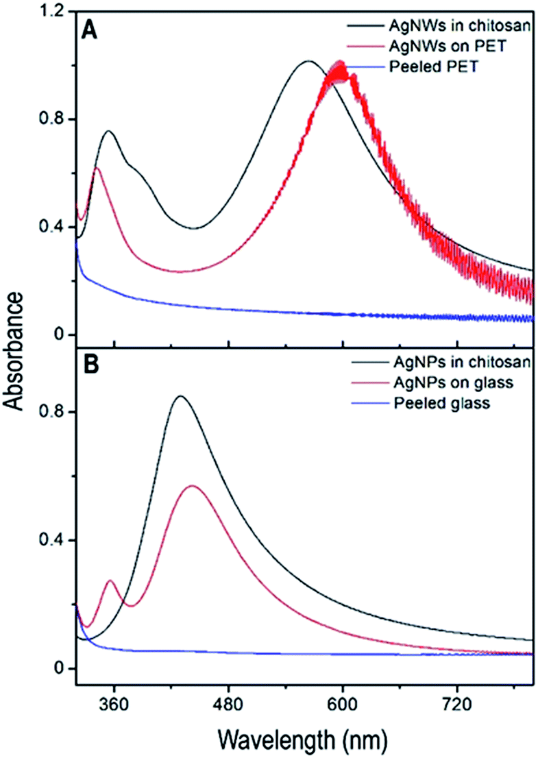 | ||
| Fig. 2 UV-Vis spectra of AgNWs on the initial PET substrate, AgNWs transferred into chitosan foil during the peeling process, and nano-patterned PET substrate after the peeling process (A). UV-Vis spectra of AgNPs on the glass substrate, AgNPs transferred into chitosan foil during the peeling process, and the glass substrate after the peeling process (B). | ||
 | ||
| Fig. 3 SEM images of individual steps of the preparation and transfer of the silver NWs: nano-patterned PET substrate prepared by laser irradiation (A), silver NWs prepared by vacuum evaporation on the nano-patterned PET substrate (B), and silver NWs transferred into chitosan foil from PET (C). | ||
 | ||
| Fig. 4 SEM images of individual steps of the preparation and transfer of silver NPs: pristine microscopic cover glass (A), silver NPs prepared by thermal annealing of sputtered silver coating on the glass substrate (B), and silver NPs transferred into chitosan foil from the glass (C). | ||
Transfer of NPs from glass to chitosan (Fig. 4) was less efficient than the transfer of NWs. Particle vacancies were observed in chitosan after the peeling (compare Fig. 4B and C). The vacancies resulted from the peeling process itself and subsequent manipulation of the sample. Nevertheless, most of the particles were still captured in the chitosan film. The concentration of vacancies, separation of solidified chitosan film from glass or other substrate, and material properties of chitosan foil (elasticity, adhesion, wettability, solubility, etc.) can be extensively modified by changing various features of the original solution, including its concentration, pH or additives.
Controlling the solubility of chitosan was another important objective of this research. Peeled chitosan foil containing silver NWs was dissolved in an acidic solution of acetate buffer (pH 4.65). Images obtained by TEM are shown in Fig. 5A. (Here, a JEOL JEM-1010 microscope was used, the images were acquired using a Megaview III digital camera, Soft Imaging Systems – Olympus, and the acceleration voltage was 80 kV.) After the dissolution of the foil, we obtained a suspension of NWs stabilized by chitosan molecules.25 The shape of the wires did not change, but some of the wires were broken into pieces with lengths of about 10 μm, but with shorter pieces as well. We suggest that this damage may have been caused by the handling of the samples during their preparation for TEM. (In this preparation process, 10 μL of chitosan solution was deposited on a copper grid covered with a thin amorphous carbon film; the excess solution was removed; and the grids were gently washed with distilled water and dried with Whatman filtration paper) It would be more convenient to transfer nanoparticles that did not have such high aspect ratios. A suspension of silver NPs is shown in Fig. 5B. The particles were observed to be not exactly uniform in size, and this lack of uniformity was due to the preparation technique. All measurements were repeated after three months to confirm that the particles did not aggregate. We were able to obtain chitosan-stabilized NP suspensions with no need of any kind of chemical (organic solvent, reducing agent, surfactant, etc.), in contrast to classic wet methods. Moreover, our transfer (peeling) method can be applied more widely than what we have described above. We successfully used this method for the transfer of various metals and even various types of substrates. Its use can be very beneficial for many researchers in various research areas, and especially in the production of nanoscale materials.
 | ||
| Fig. 5 TEM images of a dissolved chitosan foil containing silver NWs (A) and NPs (B). | ||
Conclusions
The transfer of metallic nanostructures from various kinds of solid-state substrates into chitosan foil is possible when using our peeling method. Therefore, silver nanowires and nanoparticles embedded into the surface of a biocompatible polymer can be prepared with a purely physical approach. Chitosan can be easily dissolved in a water-based solution, which enables another transfer of nanostructures into the suspension. These nanoparticles and even nanowires do not tend to aggregate, because chitosan molecules act as stabilizing agents.Acknowledgements
Financial support from Grant Agency of Czech Republic (P108/12/G108) is gratefully acknowledged.Notes and references
- V. N. Truskett and M. P. Watts, Trends Biotechnol., 2006, 24, 312–317 CrossRef CAS PubMed.
- M. Csete and Z. Bor, Appl. Surf. Sci., 1998, 133, 5–16 CrossRef CAS.
- A. Biswas, I. S. Bayer, A. S. Biris, T. Wang, E. Dervishi and F. Faupel, Adv. Colloid Interface Sci., 2012, 170, 2–27 CrossRef CAS PubMed.
- C. Marambio-Jones and E. M. Hoek, J. Nanopart. Res., 2010, 12, 1531–1551 CrossRef CAS.
- J. Siegel, K. Kolářová, V. Vosmanská, S. Rimpelová, J. Leitner and V. Švorčík, Mater. Lett., 2013, 113, 59–62 CrossRef CAS.
- T. Huang and X.-H. N. Xu, J. Mater. Chem., 2010, 20, 9867–9876 RSC.
- Y. Kalachyova, O. Lyutakov, M. Kostejn, M. Clupek and V. Švorčík, Electron. Mater. Lett., 2015, 11, 288–294 CrossRef CAS.
- M. Duval Malinsky, K. L. Kelly, G. C. Schatz and R. P. Van Duyne, J. Phys. Chem. B, 2001, 105, 2343–2350 CrossRef.
- P. Slepička, O. Neděla, J. Siegel, R. Krajcar, Z. Kolská and V. Švorčík, eXPRESS Polym. Lett., 2014, 8, 459–466 CrossRef.
- R. Krajcar, J. Siegel, P. Slepička, P. Fitl and V. Švorčík, Mater. Lett., 2014, 117, 184–187 CrossRef CAS.
- R. Krajcar, J. Siegel, O. Lyutakov, P. Slepička and V. Švorčík, Mater. Lett., 2014, 137, 72–74 CrossRef CAS.
- V. Švorčík, J. Zehentner, V. Rybka, P. Slepička and V. Hnatowicz, Appl. Phys. A: Mater. Sci. Process., 2002, 75, 541–544 CrossRef.
- V. Švorčík, J. Siegel, P. Šutta, J. Mistrík, P. Janíček, P. Worsch and Z. Kolská, Appl. Phys. A: Mater. Sci. Process., 2010, 102, 605–610 CrossRef.
- V. Švorčík, O. Kvítek, O. Lyutakov, J. Siegel and Z. Kolská, Appl. Phys. A: Mater. Sci. Process., 2011, 102, 747–751 CrossRef.
- C. V. Thompson, Annu. Rev. Mater. Res., 2012, 42, 399–434 CrossRef CAS.
- P. Farzinpour, A. Sundar, K. D. Gilroy, Z. E. Eskin, R. A. Hughes and S. Neretina, Nanotechnology, 2012, 23, 495604 CrossRef CAS PubMed.
- K. Kolářová, V. Vosmanská, S. Rimpelová, P. Ulbrich and V. Švorčík, J. Nanosci. Nanotechnol., 2015, 15, 10120–10126 CrossRef.
- L. Qian and H. Zhang, Green Chem., 2010, 12, 1207–1214 RSC.
- P. A. Sandford and A. Steinnes, Water-soluble polymers, ACS symposium series, 1991 Search PubMed.
- E. Ruel-Gariépy and J.-C. Leroux, Chitosan: a natural polycation with multiple applications, ACS symposium series, 2006 Search PubMed.
- H. Yi, L.-Q. Wu, W. E. Bentley, R. Ghodssi, G. W. Rubloff, J. N. Culver and G. F. Payne, Biomacromolecules, 2005, 6, 2881–2894 CrossRef CAS PubMed.
- J. Krstić, J. Spasojević, A. Radosavljević, M. Šiljegovć and Z. Kačarević-Popović, Radiat. Phys. Chem., 2014, 96, 158–166 CrossRef.
- A. Pinchuk, U. Kreibig and A. Hilger, Surf. Sci., 2004, 557, 269–280 CrossRef CAS.
- G. Schmidl, J. Dellith, H. Schneidewind, D. Zopf, O. Stranik, A. Gawlik, S. Anders, V. Tympel, C. Katzer and F. Schmidl, Mater. Sci. Eng., B, 2015, 193, 207–216 CrossRef CAS.
- K. Esumi, N. Takei and T. Yoshimura, Colloids Surf., B, 2003, 32, 117–123 CrossRef CAS.
| This journal is © The Royal Society of Chemistry 2016 |