Fang-Chi Hsu*a,
Ming-Kuang Hsiehb,
Chiranjeevulu Kashic,
Chen-Yu Yeh*c,
Tai-Yuan Linb and
Yang-Fang Chend
aDepartment of Materials Science and Engineering, National United University, Miaoli 360, Taiwan. E-mail: fangchi@nuu.edu.tw
bInstitute of Optoelectronic Sciences, National Taiwan Ocean University, Keelung 20224, Taiwan
cDepartment of Chemistry, Research Center for Sustainable Energy & Nanotechnology, National Chung Hsing University, Taichung 402, Taiwan. E-mail: cyyeh@dragon.nchu.edu.tw
dDepartment of Physics, National Taiwan University, Taipei 106, Taiwan
First published on 16th June 2016
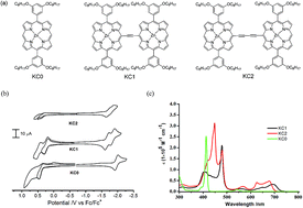
We synthesize a novel class of porphyrin dimers consisting of two zinc-metalated porphyrin units covalently linked through ethynyl (KC1) or butadiyne (KC2) group as electron donors blended with [6,6]-phenyl C70 butyric acid methyl ester (PC70BM) as electron acceptor for the fabrication of organic bulk heterojunction (BHJ) solar cells. The solution processed BHJ solar cells with porphyrin dimers:PC70BM show superior performance than those based on their parent monomer due to much broader light absorption spectra. It is found that devices with KC2:
PC70BM blend in the weight ratio of 1
:
4 exhibit higher power conversion efficiency (PCE) over those with KC1:PC70BM blend. When the KC2:PC70BM blend is processed from solvent containing 3% v/v 1-chloronaphathalene (CN), the PCE of the solar cell is improved to 2.03% from 1.73%. The superior performance and the performance improvement of the solar cells with KC2:PC70BM are due to the high short circuit current density (Jsc) resulting from a higher effective device mobility and a lower series resistance. The study provides a useful guideline for designing porphyrin based donor materials for optoelectronic device application.
Porphyrins, a subclass of small molecules, appear to be very attractive due to their importance in light harvesting for efficient energy and electron transfer process in biological system.14,15 The π-conjugated macrocyclic core of porphyrins can generate an intense Soret band at 400–450 nm and moderate Q bands at 500–650 nm. Additionally, porphyrins carry high extinction coefficient (∼105 M−1 cm−1) and their electrical and optical properties are tunable by modifying the substituents of the macrocyclic framework and/or inserting metal into the central cavity.16–18 Successful utilization of porphyrins as sensitizers in dye-sensitized solar cells19–21 and vacuum-processed solar cells22–24 have been demonstrated. Since 2007, several groups have tried to develop various soluble porphyrins25–33 as electron donors intermixed with fullerene derivatives in fabricating solution-processed BHJ OSCs and an encouraging PCE value of 8.08% has been achieved.33 These results suggest that porphyrins can be effective electron donors in BHJ OSCs and their performance could be largely improved through suitable molecular design.
To generate a large photocurrent response, sensitizers used in BHJ OSCs must have broad and strong absorption bands in the visible and near IR regions. Porphyrin dyes are promising candidates owing to their intense absorption in Soret and Q bands to harvest solar energy broadly in the visible region. However, the absorption dip between the Soret and Q bands in single porphyrins decreases their light harvesting ability and then their cell performances.
Herein, we design a class of novel porphyrin derivatives as electron donors for applications in solution-processed BHJ solar cells. We synthesize porphyrin dimers bridged with ethynyl or butadiyne having the porphyrin–π–porphyrin (KC1) or porphyrin–π–π–porphyrin (KC2) molecular architecture. The reason for our design is as follows. Linking two porphyrins with a highly conjugated bridge exhibits strong electronic coupling between porphyrin rings, leading to splitting of the Soret band and broadening of the Q bands, thus enhancing the light harvesting capability. Taking such an advantage of the spectral features, highly conjugated porphyrin dimers may be prospectively efficient sensitizers for application in OSCs. To demonstrate our thoughts, each porphyrin dimer is blended with [6,6]-phenyl C70 butyric acid methyl ester (PC70BM) as the photoactive material in solution processed BHJ OSCs. By casting porphyrin dimmer:
PC70BM blend in weight ratio of 1
:
4 from o-dichlorobenzene (ODCB), a device with the highest PCE value of 1.73% was achieved by using KC2 blend. The cell efficiency was further improved up to 2.03% when the KC2 blend was processed from a mixed solvent of 3% v/v 1-chloronaphathalene (CN) in ODCB. The superior performance and the improvement of the devices based on KC2 blend can be attributed to the high effective device mobility and the low series resistance. Those characteristics lead to higher Jsc and hence the PCE.
![]() | ||
Fig. 1 (a) Chemical structures for KC0, KC1 and KC2. (b) Cyclic voltammograms of KC0, KC1 and KC2 in THF. (c) UV-vis absorption spectra of KC-series in tetrahydrofunan. |
Fig. 1(b) depicts the cyclic voltammograms of KC series. HOMO energy levels were determined from the onset potentials of oxidations using the following equation: HOMO = −(Eonset(ox) + 4.8) eV. LUMO energy levels were calculated from the onset potentials of reductions using the following equation: LUMO = −(Eonset(red) + 4.8) eV. The onset potentials of oxidations for KC0, KC1 and KC2 were estimated to be around +0.34, +0.17, and +0.28 V, respectively, versus Fc+/Fc. These values correspond to HOMO energy levels of −5.14, −4.97, and −5.08 eV for KC0, KC1 and KC2, respectively, whereas LUMO values of KC0, KC1 and KC2 are estimated to be −2.90, −3.18, and −3.15 eV, respectively. The details for determining the energy levels for KC series are addressed in ESI.†
The UV-vis absorption spectra for KC-series in solution state exhibit a broader absorption band for dimers in contrast to two distinct narrow bands for monomer KC0, indicating the strong electron wave function coupling between porphyrin rings through the ethynyl or butadiyne bridge (see Fig. 1(c)). Those dimer dyes have intense Soret band at 400–500 nm due to characteristic π–π* transition predominantly localized at porphyrin ring. Moderate Q band with strong charge transfer character is also observed at 550–700 nm.
Since dimers show superior photon harvesting capability than monomer KC0, they are more appropriate as sensitizers in solar cells. To be an effective photoactive material to produce photoelectric effect, those dimers were blended with charge acceptor PC70BM forming a BHJ structure. Fig. 2(a) depicts the UV-vis absorption spectra for KC1, KC2, PC70BM, KC1:PC70BM and KC2:PC70BM films deposited on ZnO on quartz substrates. Thin films made from these dimers on quartz substrates absorb photons of energies in bands of blue-to-green and red regions, which also match the solution UV-vis absorption spectra. The PC70BM film absorbs the whole visible photons, which can compensate the weak absorption region of both porphyrins after inclusion. Fig. 2(b) and (c) display the surface morphology of KC1:PC70BM and KC2:PC70BM films deposited on ZnO films measured by atomic force microscopy (AFM). The KC1 blend film is composed of a connection of grains while the KC2 blend film is relatively homogeneous. The root-mean-square (rms) roughness values for KC1 and KC2 blend films are 0.615 and 0.418 nm, respectively, indicating a smooth surface feature for both films.
The performance of devices based on both KC1 and KC2 blends was evaluated and the typical J–V curves are shown in Fig. 3(a) along with the detailed performance parameters summarized in Table 1. Those parameters are averaged over at least 20 devices. The average PCE for KC1 devices is (1.15 ± 0.06)% with the highest value of 1.24% while that for KC2 devices is (1.63 ± 0.06)% with the best performance of 1.73%. Overall, KC2 devices exhibit superior performance than KC1 ones due to the significant difference in Jsc. The higher Jsc produced by KC2 devices is also reflected in the IPCE response with higher photon-to-charge conversion rate over the wavelengths of 400–800 nm (see Fig. 3(b)). For comparison, we have also tried to fabricate solar cells using porphyrin monomer blended with PC70BM as the photoactive layer and obtained the best device performance of PCE = 0.56% for Jsc, Voc, and FF of 2.9 mA cm−2, 0.65 V, and 30.2%, respectively (see Fig. S1†). As expected, the worse performance of KC0:PC70BM devices is primarily due to a much lower Jsc, which can be attributed to a much lower light absorption capability of monomer in comparison with dimers.
x:PC70BM | Jsc (mA cm−2) | Voc (V) | FF (%) | PCE (%) |
---|---|---|---|---|
KC1 | 5.22 ± 0.21 (5.3) | 0.72 ± 0.03 (0.76) | 30.38 ± 0.39 (30.7) | 1.15 ± 0.06 (1.24) |
KC2 | 6.60 ± 0.32 (6.8) | 0.79 ± 0.05 (0.78) | 31.33 ± 0.95 (32.6) | 1.63 ± 0.06 (1.73) |
KC2:CN | (7.7) | (0.80) | (32.8) | (2.03) |
It has been reported35,36 that porphyrin films prepared from additive contained solvent can effectively enhance the performance of devices. We choose KC2:PC70BM blend of relatively higher performance for demonstration. The corresponding J–V curve for the KC2 blend casted from mixture solvent containing 3 v% of CN in comparison with additive-free case is also shown in Fig. 3(a) and the corresponding parameters for the best device is summarized in Table 1 as well. It clearly shows that there is an ∼13% enhancement in Jsc relative to the additive-free device while the improvements in Voc and FF are subtle. A PCE value of 2.03% has been achieved, an ∼24.5% enhancement compared with the additive-free one. The largely enhanced Jsc for KC2:PC70BM:CN device is also confirmed by the IPCE result shown in Fig. 3(b).
To elucidate the higher and the improvement of Jsc for KC2 devices, we have conducted the transient photocurrent measurement to evaluate the effective device mobility for KC1, KC2, KC2:CN blend devices.37 Fig. 3(d) displays the short-circuit current response of those three devices to 200 μs square-pulse optical excitation from a 530 nm green-light LED driven by a matching driver. Photocurrent is displayed as current instead of current density because the illumination size of the light spot is within the area of the devices. Apparently, there is a fast turn-on and turn-off dynamics for those three samples. To calculate the effective device mobility, we first determine the effective transit time τt as the period of time required for photocurrent to decay to 1/e of its equilibrium value. Then, the effective device mobility (μ) can be calculated from μ = d/(Eτt), where d is the thickness of the photoactive layer, and E is the internal electric field. The internal electric field can be calculated from 1/E = d/(Vbi − Va), where Vbi (∼0.8 V) and Va are the build-in voltage and applied voltage (0 V), respectively. The estimated mobility values for KC1, KC2, and KC2:CN devices are 7.6 × 10⁻⁴, 9.0 × 10⁻⁴, and 1.3 × 10⁻³ cm2 V−1 s−1, respectively. The effective device mobility value follows the order KC1 < KC2 < KC2:CN, which is consistent with the trend for Jsc.
Based on the above results, the performance of porphyrin dimers can be understood as follows. Both dimer:PC70BM films are of similar light absorption capability, but carry different surface features as shown in Fig. 2(b) and (c). In an organic solar cell, an effective photoactive layer is prepared by mixing organic donors and acceptors to create a BHJ structure. Those donors and acceptors form bi-continuous carrier transport pathways for carrier traveling. Fortunately, each arrangement of pathway can be quantified by either carrier mobilities or the effective device mobility (μ), depending on the measurement technique used. In some cases, those microscopically distinct arrangements can result in different surface morphologies on the macroscopic level. As found that the surface texture of the KC1:PC70BM film is composed of a collection of grains in contrast to the homogeneous morphology of the KC2:PC70BM one, it is highly probable for carriers to be trapped at the grain boundary resulting in lower μ. For the KC2:PC70BM:CN film, we have also measured its surface morphology (see Fig. S2†) and the image exhibits similar surface feature and rms roughness value (0.499 nm) to those for KC2:PC70BM. Though there is no apparently macroscopic difference in the surface morphology between these two films, the higher μ of the KC2:PC70BM:CN film indicates that CN molecules play an important role in the assembling process of KC2 and PC70BM molecules on the microscopic level. Therefore, the architecture of BHJ created by mixing donors and acceptors is important for transporting carriers. The higher μ can lead to larger Jsc.
Alternatively, the distinct assembled structure among KC1, KC2, and KC2:CN blends can result in different bulk resistance and is also discernible from the series resistance (Rs) on a device level. We calculated Rs of each device by taking the reciprocal of the slope at Voc from the measured J–V curve. The obtained values for Rs were 63.9, 50.6, and 45.3 Ω cm2 for KC1, KC2, and KC2:CN devices, respectively. Apparently, the bulk resistance of the photoactive layer follows the order KC2:CN < KC2 < KC1, suggesting that the mixing result of KC2:CN blend forms the lowest resistivity pathways for carrier transport, and hence the higher μ and Jsc.
As the energy band diagram shown in Fig. 3(d), KC1 (or KC2):PC70BM device forms cascaded energy structures both in HOMO and LUMO levels for transporting electrons and holes. It has been reported38 that the theoretical value of Voc is the difference between the LUMO of acceptor (EALUMO) and the HOMO of donor (EDHOMO). Based on Fig. 3(d), EALUMO − EDHOMO = 0.97 and 1.08 eV for KC1 and KC2 devices, respectively. The larger Voc value in KC2 blend from theoretical prediction is consistent with the experimental observation. The lower experimentally obtained values of Voc for all devices may be due to space charge formation within devices through trapping states at porphyrin–metal oxide interface or within the photoactive layer resulting in internal voltage dropping.
It is noted that porphyrin–π–π–porphyrin (KC2) molecular architecture demonstrates a superior light-to-power conversion efficiency over porphyrin–π–porphyrin (KC1) one for a higher effective device mobility when mixed with PC70BM. We have also measured the intrinsic mobilities of KC1 and KC2 using the space-charge-limited-current (SCLC) method.39 By analyzing the current response across the hole-only structure of ITO/PEDOT:PSS/KC1 (or KC2)/MoO3/Ag (see Fig. S3†), we obtain that the intrinsic mobilities of KC1 and KC2 are 4.5 × 10⁻⁴ and 6.3 × 10⁻⁴ cm2 V−1 s−1, respectively. It is found that KC2 with a longer π-conjugation bridge possesses higher intrinsic carrier mobility as well as higher effective device mobility in a blend film. The result indicates that an extended π-conjugation pathway between porphyrin rings is beneficial for carrier transport. On the other hand, from the engineering viewpoint of device design, one of the possible strategies to further improve the device performance is to tune the surface properties of the metal-oxide layer in order to enhance the electrical coupling between organic/inorganic interface and extract charges out of the photoactive layer. This issue of surface engineering is currently under study in our laboratory. Our study can provide a useful guideline for designing porphyrin based donor materials for solar cell application and advance the development of other optoelectronic devices.
Footnote |
† Electronic supplementary information (ESI) available: Synthesis procedures, cyclic voltammetry, absorption spectra, and device performance. See DOI: 10.1039/c6ra04746g |
This journal is © The Royal Society of Chemistry 2016 |