DOI:
10.1039/C6RA04743B
(Paper)
RSC Adv., 2016,
6, 42413-42420
Promising photovoltaic application of multi-walled carbon nanotubes in perovskites solar cells for retarding recombination
Received
25th February 2016
, Accepted 14th April 2016
First published on 15th April 2016
Abstract
A facile spray deposition method was developed to prepare a high-quality perovskite layer under ambient conditions. However, the performance is expected to be further improved with substrate and the hole transport layer (HTL) optimization and device structure, for instance. MWCNTs with incorporated spiro-OMeTAD exhibited Jsc of 22.13 mA cm−2 and PCE of 10.42%. To infer the origin of the increasing Jsc and PCE, the optical absorption performance, charge transfer and recombination performance were investigated. τ, Rct, Rrec as a function of voltage and EIS measurements revealed the lower transfer resistance and recombination rate in PSCs with MWCNTs compared with the PSCs without MWCNTs. The increased resistance in dark conditions and the dark J–V curves explain the slight changes in the Voc. The SEM images showed that there were no MWCNTs aggregated on the surface of the spiro/MWCNTs composite layer and part of MWCNTs was uncovered by spiro-OMeTAD at the interface of HTM and Au electrode. The decreased ID/IG ratio from 0.90 to 0.68 demonstrated the increased interaction between MWCNTs and spiro-OMeTAD.
1. Introduction
Since the first report based on organic–inorganic hybrid perovskites CH3NH3PbBr3 and CH3NH3PbI3 with a 3.8% efficiency in 2009,1 their efficiencies have leaped to 20.1% in 2014,2,3 which were comparable with Cu(In, Ga)Se2 solar cells.4 However, some problematic issues need to be resolved, for example, the most representative hole transport spiro-OMeTAD materials are expensive and need p-type doping to enhance the fabrication cost and mitigate possible instability, the commonly employed electron transport material, TiO2, still requires high-temperature processing to increase the crystallinity and achieve suitably high charge carrier mobility, and the metal electrode is relatively expensive and deposited by high-vacuum thermal evaporation.
Carbon materials, such as graphene oxide (GO), carbon nanotubes (CNTs), fullerene (C60), and graphdiyne (GD), were chosen for application in perovskite solar cells (PSCs) because of their excellent thermal, mechanical, electrical and optical performance. Carbon materials have been applied in highly efficient counter electrodes, in solid state electrolyte and in photoanodes with an engineered interfacial layer for dye-sensitized solar cells5–7 and organic solar cells.8–11 The approximate 5.0 eV work function makes carbon materials ideal PSCs counter electrode materials. Wong et al.12 introduced a facile perovskite solar cell by directly laminating CNTs films onto a CH3NH3PbI3 substrate with an efficiency of 9.9%. Meng et al.13,14 fabricated an all-carbon counter electrode for hole-conductor-free PSCs by a simple and low-temperature process. Han et al.15 developed fully printable mesoscopic PSCs based on TiO2/ZrO2/carbon, with an efficiency exceeding 13%.
Carbon materials can be endowed with a remarkably high charge mobility and electronic conductivity and have been identified as one of the strongest materials for electron transport in PSCs. Snaith et al.16–18 replaced TiO2 with a C60 self-assembled monolayer and GO, respectively, which showed the potential to contribute significantly towards developing low-cost and long-term operationally stable PSCs.
Similarly, a perovskite solar cell using hole transport materials incorporating carbon materials showed improved power conversion efficiency due to enhanced electrical conductivity and carrier mobility. This was because the low electrical conductivity of hole transport materials was considered an impediment to further enhancements of the power conversion efficiencies and a hole transport material with higher conductivity should decrease the series resistance and increase the fill factor, thus enhancing the PSCs power conversion efficiency. Meng and Li19 employed GD as a p-type dopant to modify P3HT and revealed that a relatively strong π–π stacking interaction occurred between GD particles and P3HT and some GD aggregates exhibited a scattering nature, which were favorable for improving the cell performances. Wang et al.20 applied GO as dual functional modifier on the interface of perovskite and spiro-OMeTAD. These results illustrated that GO interacted with perovskite by forming Pb–O bonds and absorbed spiro-OMeTAD via π–π interactions. Baik et al.21 deposited a perovskite layer by a toluene drop-casting method and embedded CNTs into spiro-OMeTAD to increase carrier mobility and conductivity. They focused on the effect of hierarchical structure and CNTs concentration on cell performance, showing an improved efficiency as CNTs concentrations were increased from 0 to 2 wt%.
In this study, we intended to prepare high-quality perovskite layer by a facile spray deposition method under ambient condition with a high humidity of up to 50%, which provided a novel strategy for scalable and fast fabrication of high-quality absorber layers for efficient PSCs and exhibited an efficiency of 7.89% in the previous study.22 However, the performance was expected to be further improved with the increase of substrate temperature, by utilizing more compatible substrates and optimizing the hole transport layer (HTL) and device structure. Except for the high electrical conductivity and carrier mobility, MWCNTs are low-cost and highly available industrial materials. Herein, we employed MWCNTs into the HTL such as spiro-OMeTAD and focused on the charge transfer and recombination performance and the interaction between MWCNTs and spiro-OMeTAD.
2. Experimental
2.1 Materials and sample preparation
Purified MWCNTs (ID: 2–5 nm, OD: <8 nm, length: 0.5–2 μm, purity: >95 wt%) was supplied by Chengdu Organic Chemicals Co., Ltd. An equal molar ratio of CH3NH3I and PbI2 was dissolved in 4 mL anhydrous N,N-dimethylformamide (DMF) and stirred at room temperature for 2 h, producing a CH3NH3PbI3 precursor solution with an 11.25 wt% concentration. The pure spiro-OMeTAD (supplied by Xi'an Polymer Light Technology Corp) solution was prepared according to a literature method.21 2 wt% MWCNTs was added into the spiro-OMeTAD solution with stirring for 1 h to achieve a spiro/MWCNTs solution. To obtain spiro/MWCNTs powders for testing, 2 mg of spiro-OMeTAD was mixed with 5 mg of MWCNTs in chlorobenzene and the mixture was dried under vacuum at 60 °C for 24 h.
2.2 Device fabrication
A TiO2 compact layer was deposited onto a fluorine-doped SnO2 (FTO)-coated glass substrate (etched with zinc powder and hydrochloric acid) by spray pyrolysis at 450 °C, followed by a TiO2 mesoporous layer applied with a spin coating method at 4000 rpm for 40 s and then thermal annealing at 80 °C for 15 min. To prepare the perovskite film, the TiO2-coated substrate was held on a hot plate at 110 °C and then the CH3NH3PbI3 precursor solution was sprayed onto the substrate in an ambient atmosphere. To prepare the HTL by two-step spin coating, 20 μL of pure spiro-OMeTAD solution was spin coated onto the perovskite film at 4000 rpm for 30 s, followed by 20 μL of pure spiro-OMeTAD solution for the non MWCNTs-based device and 20 μL spiro/MWCNTs solution for the spiro/MWCNTs-based device. Subsequently, Au was magnetron sputtered as the cathode onto the HTL film.
2.3 Characterizations
The photocurrent–voltage (J–V) curves, electron lifetime–voltage (τ–V) curves and electrochemical impedance spectra (EIS, from 0.05 to 120 kHz) were obtained using an electrochemical workstation (AUTOLAB TYPE II) with a solar simulator (ABET Sun 3000) and source meter (Keithley 2420) at 100 mA cm−2 illumination (AM 1.5 G). The mask active area was 0.0672 cm−2. The resulting EIS were fitted using ZView software. The UV-vis absorption spectra were obtained on a Perkin-Elmer spectrophotometer (Lambda 750). The morphology and cross-section characterization were performed with a high resolution field emission scanning electron microscope (FESEM, S4800). Fourier transform infrared spectrum was obtained with a spectrometer (FTIR, TENSOR27). The Raman spectra were obtained using a Raman spectrometer (LabRAM HR800-LS55) with a 532 nm laser.
3. Results and discussions
3.1 J–V curves and optical absorption performance
The J–V characteristics for PSCs containing MWCNTs in comparison with those of PSCs without MWCNTs under simulated AM 1.5 G solar irradiation are shown in Fig. 1 and Table 1. The short circuit current density (Jsc) of 22.13 mA cm−2 and power conversion efficiency (PCE) of 10.42% has been observed for the PSCs that incorporated MWCNTs. The open circuit voltage (Voc) of the two cells slightly changed. To infer the origin of increasing Jsc and Voc, the optical absorption performance, charge transfer and recombination performance were investigated.
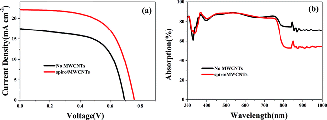 |
| | Fig. 1 (a) The photocurrent density–voltage (J–V) curves and (b) the UV-vis spectra of PSCs containing MWCNTs and without MWCNTs. | |
Table 1 The photovoltaic performance of PSCs containing MWCNTs and without MWCNTs
| |
Jsc (mA cm−2) |
Voc (V) |
FF |
PCE (%) |
| No MWCNTs |
17.50 |
0.70 |
0.62 |
7.53 |
| Spiro/MWCNTs |
22.13 |
0.76 |
0.62 |
10.42 |
Fig. 1b presents the UV-vis spectra of PSCs with and without MWCNTs content. Both devices exhibited a strong and broad absorption from the visible to the near infrared and in addition to that the spectra for the two devices were almost identical and covered a good part in the visible region from 300 nm to 750 nm.
3.2 Electron lifetime and charge transfer
The charge recombination properties of the PSCs can be investigated from electron lifetime–voltage (τ–V) curves (Fig. 2a) based on the transient Voc decay experiment. The electron lifetime could be derived from the photovoltage decay curve according to the following formula:23| |
 | (1) |
where kB is the Boltzmann constant, T is the absolute temperature and q is the positive elementary charge. The electron lifetime τ had a variation tendency similar to that of the recombination resistance in light. The decrease in τ at higher light intensity is attributed to relatively faster recombination. In Fig. 2a, we can observe that the τ for the PSCs without MWCNTs was clearly lower than that with MWCNTs. Therefore, the recombination in PSCs without MWCNTs was faster compared to the recombination in the PSCs with MWCNTs in light. The faster recombination explains the lower Voc and Jsc of the PSCs without MWCNTs.
 |
| | Fig. 2 (a) The electron lifetime–voltage (τ–V) curves and (b) recombination resistance based on formula (2) of PSCs containing MWCNTs and without MWCNTs under illumination. | |
In general, the resistance is a derivative of the J–V curve. As a small perturbation voltage, ΔV, and a current response, ΔJ, are applied to the cell, the charge transfer resistance of the cell can be derived as:24,25
| |
 | (2) |
where
A is the ideality factor,
kB is the Boltzmann constant,
T is the thermodynamic temperature,
q is the elementary charge and
J0 is the dark current density and is used to estimate the
Voc of a cell as follows:
26| |
 | (3) |
Usually, a large Rct reflects a small charge transfer and recombination rate in the cell, leading to a high Voc. For PSCs with MWCNTs, the Rct increased largely, which meant the charge recombination was decreased, i.e., it could prevent the electrons in perovskites from recombining with holes left in the hole transport layer. Little current loss during the charge transfer process occurred, giving an enhanced Jsc. Otherwise, the reported carrier concentration and mobility of the MWCNTs was 1.94 × 1019 cm−3 and 220 cm2 V−1 s−1, respectively, which are higher than those of spiro-OMeTAD (7.13 × 1015 cm−3 and 0.779 cm2 V−1 s−1, respectively).21,27 The CNTs incorporated in spiro-OMeTAD resulted in an increase in the electron mobility and therefore balanced the charge carrier transport to the metal electrodes.
3.3 Electrochemical impedance spectra under illumination
Electrochemical impedance spectroscopy (EIS) was carried out to measure the electric response under bias voltage or illumination, which is highly critical in the investigation of charge transfer and recombination properties in a cell. Under full illumination, the Nyquist plot (Fig. 3) showed typical semicircles in the frequency range of 0.5–120 kHz with a 0.8 V and 0 V voltage bias. The first remarkable fact is that similar impedance patterns were obtained for the two cells with the same bias voltage. The EIS spectra at high frequency may contain information of transport and series resistance elements, as well as dielectric contributions. The low frequency arc is attributed to recombination in the photoactive blend.28 The first arc is related to the selective contact, including electron-selective contact and hole-selective contact. The selective contacts have the function of taking the carriers from a state of a non-equilibrium Fermi level in the absorber to a material in which the carrier is at the equilibrium Fermi level.29 For the PSCs with MWCNTs and without MWCNTs, the electron-selective contact was not changed and therefore the hole-selective contact enhanced with MWCNTs addition.
 |
| | Fig. 3 Nyquist plots for impedance spectra biased at (a) 0 V and (b) 0.8 V. | |
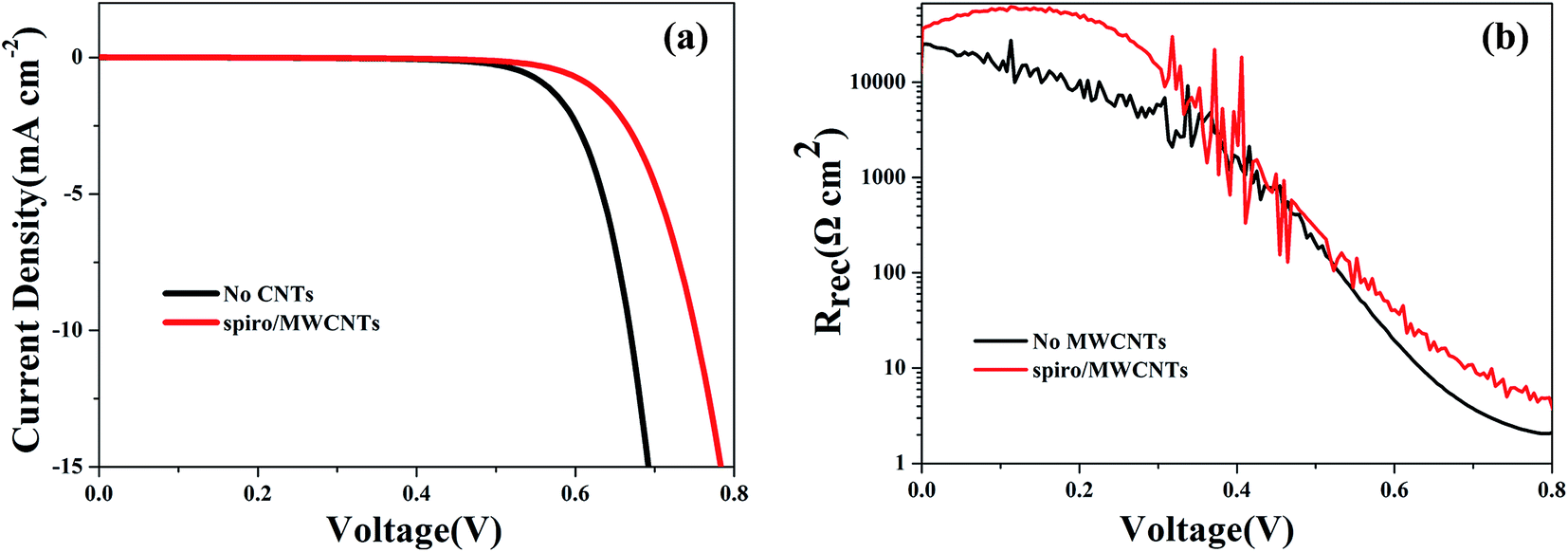
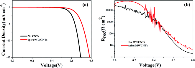
3.4 J–V curves in the dark and charge recombination
Fig. 4 showed the J–V curves of PSCs containing MWCNTs compared with those PSCs without MWCNTs tested in dark conditions. The onset of PSCs containing MWCNTs moved to nearly 0.2 V higher voltage, which indicated that the back flow of electrons from TiO2 to the perovskite layer or the hole conductor was significantly suppressed.
 |
| | Fig. 4 (a) J–V curves and (b) recombination resistance according to formula (4) of PSCs containing MWCNTs and without MWCNTs under dark conditions. | |
Important information about the charge recombination in PSCs is contained in the overall recombination resistance, Rrec, as observed in Fig. 4b, which was derived from the formula (4).30,31 The Rrec produces a rather direct view of the recombination process, showing directly the exponential variation of the recombination rate. At high voltages, the dominant mechanism is charge recombination and at low voltages and charge transfer from the back layer dominates. It is obvious that the PSCs with MWCNTs present higher Rrec (lower recombination rate) than the PSCs without MWCNTs, which is an important feature to explain the difference in these two cells, corresponding to delivering the efficiency from 7.53% to 10.56%.
| |
 | (4) |
3.5 Electrochemical impedance spectra under dark condition
To force the photovoltaic device to mainly operate under recombination conditions, one can perform EIS measurements under open-circuit conditions. Under such conditions, no direct current is allowed so that the transport mechanisms play a secondary role. In the dark conditions, the Nyquist plot of the impedance spectra was obtained in a frequency range of 0.5–120 kHz with 0.5, 0.6, 0.7 and 0.8 V bias voltages, respectively, as shown in Fig. 5. In the equivalent circuit model12 (Fig. 6a), R1 is the related recombination resistance and CPE1 is the chemical capacitance of the film; R2 and CPE2 are related to the HTL resistance, capacitance and the extraction in the Au electrode. The resistance of the main arc is the combination resistance.25,32 The R1 and R2 value were demonstrated in Fig. 6b and c, which was fitted with ZView software according to the equivalent circuit model. In general, increased resistance in dark conditions indicates a restrained charge recombination. This was verified by the dark J–V curves, as shown in Fig. 4a. Moreover, the changes in the Voc can reveal the extent of delayed electron recombination, which can be explained by formula (3). In addition to that the actual value of Voc was strongly influenced by the shape of the density-of-states, which determines the position of the Fermi level as well.29,33
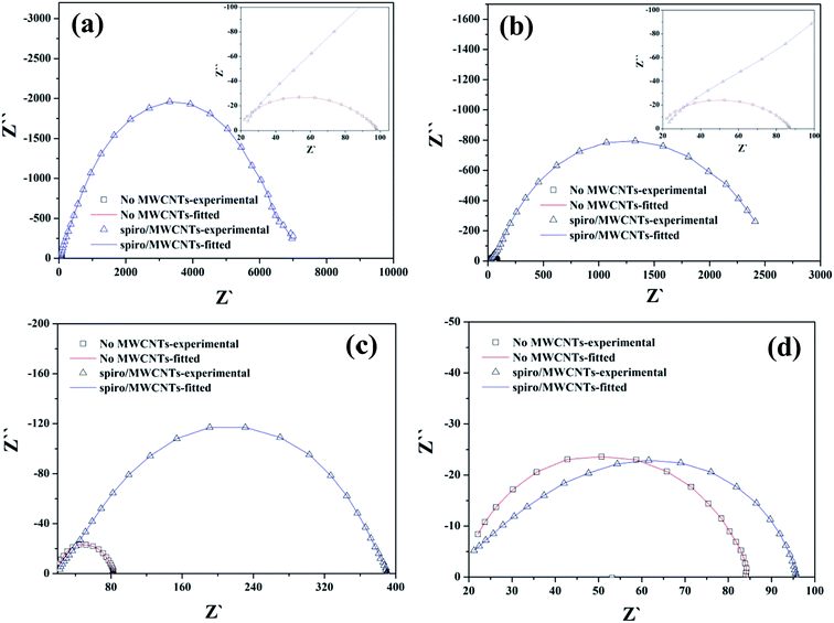 |
| | Fig. 5 Nyquist plots of impedance spectra biased under dark conditions at (a) 0.5 V; (b) 0.6 V (c) 0.7 V; and (d) 0.8 V. | |
 |
| | Fig. 6 (a) The equivalent circuit model applied in these PSCs; (b) R1 and (c) R2 value fitted with ZView software based on the equivalent circuit model. | |
3.6 Morphology and device structure
As is well known, one of the main challenges in PSCs is fabricating high quality films with controlled morphology, high surface coverage and minimal pin-holes. The SEM images of perovskite films prepared by spray deposition had full coverage on the TiO2 substrate with the absence of pin-holes, as observed in Fig. 7a. Fig. 7b–d shows the SEM images of HTL film on perovskites. There was no MWCNTs aggregate on the surface of the spiro/MWCNTs composite layer and part of the MWCNTs was uncovered by spiro-OMeTAD at the interface of HTM and Au electrode. As shown in Fig. 7e, the whole thickness of perovskite film and HTL layer was about 800 nm and 100 nm, respectively. The complete device structure is demonstrated schematically in Fig. 7f. It is worth noting that the HTL comprises two parts: one is a uniform spiro-OMeTAD layer and the other is a spiro/MWCNTs composite layer.
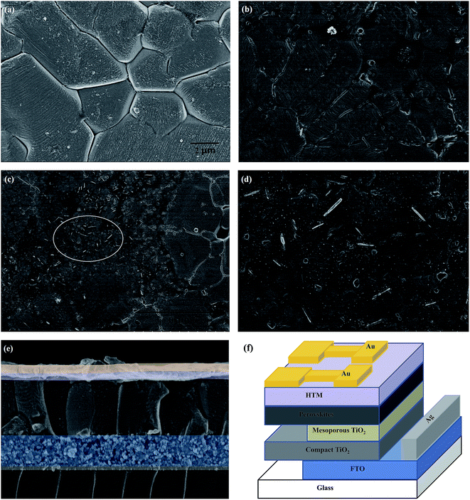 |
| | Fig. 7 SEM images of (a) perovskite film on a TiO2 substrate; (b) uniform spiro-OMeTAD layer on a perovskite film; (c) and (d) spiro/MWCNTs composites on uniform spiro-OMeTAD layer; (e) cross-sectional images of the device structure; (f) schematic of the whole device. | |
3.7 Interaction between MWCNTs and spiro-OMeTAD
To confirm interaction between MWCNTs and spiro-OMeTAD, the FT-IR spectra of MWCNTs, spiro-OMeTAD and their composites were obtained and are displayed in Fig. 8a. The intensity difference between MWCNTs and spiro/MWCNTs composites is probably because of the different contents from the sample preparation. The peak at 3500 cm−1 is characteristic of –OH groups existing in MWCNTs. The peaks in the transmittance spectrum for methoxy phenyl assigned to spiro-OMeTAD could be observed at 1602, 1498, 1466 and 1248 cm−1. The MWCNTs performed as a base absorbing the spiro-OMeTAD onto its surface. This was further verified by the Raman spectra, as shown in Fig. 8b. The two broad peaks at 1350 and 1580 cm−1 are usually attributed to sp3 and sp2 bonding, which are recognized as ID and IG, respectively. The decreased ratio of ID/IG from 0.90 to 0.68 as MWCNTs incorporated with spiro-OMeTAD illustrated an increased interaction between the MWCNTs and spiro/MWCNTs because of the π–π conjugation.
 |
| | Fig. 8 (a) FT-IR spectra and (b) Raman spectra of MWCNTs and spiro/MWCNTs composites. | |
4. Conclusions
MWCNTs incorporating spiro-OMeTAD achieved a Jsc of 22.13 mA cm−2 and PCE of 10.42% with a high-quality perovskite layer prepared by a facile spray deposition method under ambient condition with up to 50% high humidity. Compared with the PSCs without MWCNTs, the UV-vis spectra for the two devices were almost identical and covered a good part in the visible region from 300 nm to 750 nm. However, the transfer resistance and recombination rate in PSCs with MWCNTs was lower according to the τ, Rct, Rrec as a function of voltage and EIS measurements so that little current was lost during the charge transfer process giving an enhanced Jsc and a corresponding efficiency ranging between 7.53% and 10.56%. Moreover, the slight changes in the Voc could be explained by the increased resistance in dark conditions, which was further verified by the dark J–V curves, revealing the extent of delayed electron recombination. The SEM images show that there were no MWCNTs aggregated on the surface of the spiro/MWCNTs composite layer and part of MWCNTs was uncovered by spiro-OMeTAD at the interface of HTM and Au electrode. The increased interaction between MWCNTs and spiro-OMeTAD was confirmed by their FT-IR spectra and Raman spectra because of the decreased ratio of ID/IG from 0.90 to 0.68.
Acknowledgements
Project supported by Project on the Collaborative Innovation and Environmental Construction Platform of Guangdong Province (2014A050503051), the National Natural Science Foundation of China (21073193, 21273241), Jiangsu Province Industry-University-Research Joint Innovation Fund (BY2013024-01), and the Open Fund of Jiangsu Key Laboratory of Materials and Technology for Energy Conversion (MTEC-2015M01) and the Natural Science Foundation of Guangdong Province (2015A030310501).
References
- A. Kojima, K. Teshima, Y. Shiraiand and T. Miyasaka, J. Am. Chem. Soc., 2009, 131, 6050–6051 CrossRef CAS PubMed.
- H. P. Zhou, Q. Chen, G. Li, S. Luo, T. B. Song, H. S. Duan, Z. R. Hong, J. B. You, Y. S. Liu and Y. Yang, Science, 2014, 345, 542–546 CrossRef CAS PubMed.
- M. A. Green, A. Ho-baillieand and H. J. Snaith, Nat. Photonics, 2014, 8(7), 506–514 CrossRef CAS.
- S. S. Hegedusand and W. N. Shafarman, Progress in Photovoltaics: Research and Applications, 2004, 12(12), 155–176 CrossRef.
- M. R. Golobostanfard and H. Abdizadeh, Microporous Mesoporous Mater., 2014, 191, 74–81 CrossRef CAS.
- J. Cai, Z. Chen, J. Li, Y. Wang, D. Xiang, J. Zhang and H. Li, AIP Adv., 2015, 5, 253–261 Search PubMed.
- L. Qiu, Q. Wu, Z. Yang, X. Sun, Y. Zhang and H. Peng, Small, 2014, 11, 1150–1155 CrossRef PubMed.
- H. A. Alturaif, Z. A. Alothman, J. G. Shapterand and S. M. Wabaidur, Molecules, 2014, 19, 11734–17329 CrossRef PubMed.
- T. Ji, L. Tan, X. Hu, Y. Dai and Y. Chen, Phys. Chem. Chem. Phys., 2015, 17, 4137–4145 RSC.
- N. Chehata, A. Ltaief, R. Bkakri and A. Bouazizi, Mater. Sci. Semicond. Process., 2014, 22, 7–15 CrossRef CAS.
- X. Hu, L. Chen, Y. Zhang, Q. Hu, J. Yang and Y. Chen, Chem. Mater., 2014, 26, 6293–6302 CrossRef CAS.
- Z. Li, S. A. Kulkarni, P. P. Boix, E. Shi, A. Cao, K. Fu, S. K. Batabyal, J. Zhang, Q. Xiong and L. H. Wong, ACS Nano, 2014, 8, 6797–6804 CrossRef CAS PubMed.
- Y. Yang, J. Xiao, H. Wei, L. Zhu, D. Li, Y. Luo, H. Wu and Q. Meng, RSC Adv., 2014, 4, 52825–55283 RSC.
- H. Wei, J. Xiao, Y. Yang, S. Lv, J. Shi, X. Xu, J. Dong, Y. Luo, D. Li and Q. Meng, Carbon, 2015, 93, 861–868 CrossRef CAS.
- T. Liu, L. Liu, M. Hu, Y. Yang, L. Zhang, A. Mei and H. Han, J. Power Sources, 2015, 293, 533–538 CrossRef CAS.
- J. T. Wang, J. M. Ball, E. M. Barea, A. Abate, J. A. Alexander-webber, J. Huang, M. Saliba, I. Mora-sero, J. Bisquert and H. J. Snaith, Nano Lett., 2014, 14, 724–730 CrossRef CAS PubMed.
- A. Agnese, S. D. Stranks, P. Docampo, Y. Hin-lap, K. J. Alex and H. J. Snaith, Nano Lett., 2013, 13, 3124–3128 CrossRef PubMed.
- K. Wojciechowski, T. Leijtens, S. Siprova, C. Schlueter, M. T. Hörantner, T. W. Wang, C. Z. Li, K. Y. Jen, T. L. Lee and H. J. Snaith, J. Phys. Chem. Lett., 2015, 6, 2399–2405 CrossRef CAS PubMed.
- J. Xiao, J. Shi, H. Liu, Y. Xu, S. Lv, Y. Luo, D. Li, Q. Meng and Y. Li, Adv. Energy Mater., 2015, 5, 1401943–1401950 Search PubMed.
- W. Z. Li, H. P. Dong, X. D. Guo, N. Li, J. W. Li, G. D. Niu and L. D. Wang, J. Mater. Chem. A, 2014, 2, 20105–22011 CAS.
- J. Lee, M. M. Menamparambath, J. Hwang and S. Baik, ChemSusChem, 2015, 8, 2358–2362 CrossRef CAS PubMed.
- Z. Liang, J. N. Ding, S. H. Zhang, X. Xu, N. Wang, J. Wang, X. Wang, Z. Bi, G. Xu and N. Yuan, RSC Adv., 2015, 5, 60562–60569 RSC.
- B. Juan, Z. Arie, G. Miri and M. S. Iván, J. Am. Chem. Soc., 2004, 126, 11355–13550 Search PubMed.
- J. Shi, X. Xu, D. Li and Q. Meng, Small, 2015, 11, 2472–2486 CrossRef CAS PubMed.
- J. You, Z. Hong, Y. M. Yang, Q. Chen, M. Cai, T. B. Song, C. C. Chen, S. Lu, Y. Liu, H. Zhou and Y. Yang, ACS Nano, 2014, 8, 1674–1680 CrossRef CAS PubMed.
- T. Stergiopoulos, S. Karakostas and P. Falaras, J. Photochem. Photobiol., A, 2004, 163, 331–340 CrossRef CAS.
- D. Suh, D. Lee, C. Kang, I. J. Shon, W. Kim and S. Baik, J. Mater. Chem., 2012, 22, 21376–22138 RSC.
- G. Garcia-belmonte, A. Munar, E. M. Barea, J. Bisquert, I. Ugarte and R. Pacios, Org. Electron., 2008, 9(5), 847–851 CrossRef CAS.
- G. Garcia-belmonte, P. P. Boix, J. Bisquert, M. Lenes, H. J. Bolink, A. L. Rosa, S. Filippone and N. Martín, J. Phys. Chem. Lett., 2010, 1, 2566–2571 CrossRef CAS.
- V. Gonzalez-pedro, E. J. Juarez-perez, W. Arsyad, E. M. Barea, F. Fabregat-santiago, I. Mora-sero and J. Bisquert, Nano Lett., 2014, 14, 888–893 CrossRef CAS PubMed.
- X. Xu, Q. Wan, C. Luan, F. Mei, Q. Zhao, P. An, Z. Liang, G. Xu and J. A. Zapien, ACS Appl. Mater. Interfaces, 2013, 5, 10605–11061 CAS.
- H. S. Kim, I. Mora-sero, V. Gonzalez-pedro, F. Fabregat-santiago, E. J. Juarez-perez, N. G. Park and J. Bisquert, Nat. Commun., 2013, 4, 375–381 Search PubMed.
- G. Garcia-belmonte and J. Bisquert, Appl. Phys. Lett., 2010, 96, 113301–113310 CrossRef.
Footnote |
| † The authors contributed equally to this work. |
|
| This journal is © The Royal Society of Chemistry 2016 |
Click here to see how this site uses Cookies. View our privacy policy here.