DOI:
10.1039/C6RA04584G
(Paper)
RSC Adv., 2016,
6, 31769-31774
Design and sol–gel preparation of a six-layer tri-wavelength ORMOSIL antireflective coating for a high power laser system†
Received
20th February 2016
, Accepted 22nd March 2016
First published on 24th March 2016
Abstract
A six-layer tri-wavelength antireflective (TWAR) coating possessing nearly 100% transmittance simultaneously at 1064 nm, 532 nm and 355 nm was designed and realized by a simple sol–gel process. This TWAR coating consisted of six alternating layers of two quarterwave low refractive index components. The refractive indices of these two these two components are 1.21 and 1.14. Organically modified silicate (ORMOSIL) thin films with a refractive index of 1.21–1.13 were prepared by using tetramethylorthosilicate (TEOS) and dimethyldiethoxysilane (DDS) as co-precursors. A discussion of the crack problem on the interfaces of the multi-layer sol–gel silica AR coating was proposed, which was very important in the preparation of the multi-layer AR coating with high transmittance. Finally, the designed six-layer ORMOSIL TWAR coating was realized with a transmittance of 99.7%, 99.5% and 99.2% at 355 nm, 532 nm and 1064 nm, respectively. This is the best TWAR coating so far and will find great application in a high power laser system.
1. Introduction
Antireflective (AR) coatings have been widely used in optical devices.1–5 Among the AR coatings, the single-layer sol–gel silica AR coating is very important in a high power laser system because it possesses the advantages of nearly 100% transmittance, high laser-induced damage threshold (LIDT), easy deposition in a large area and easy control of film thickness.6–8 Over the past few decades, many research studies about the improvement of environmental resistance,9–11 abrasion resistance12–15 and LIDT8,16,17 of sol–gel single-layer silica AR coatings have been carried out. However, little attention was paid to the preparation of a kind of AR coating which was called as tri-wavelength AR coating in recently. In the high power laser systems, there are some transmissive components need to transmit double wavelengths or three wavelengths of lasers with very high efficiency.18 This requires multi-layer AR coating designs because the sol–gel silica single-layer AR coating can work only at a single wavelength. A double-layer double-wavelength AR coating has been proposed by Thomas for the first time,18 and an optimized one was reported by our research group recently.19 So far, the design and preparation of TWAR coating is rarely reported. Many papers published the preparation of multi-layer broadband AR coatings.20–26 These broadband AR coatings had fairly high transmittance at an entire broad wavelength. However, none of them could arise three transmission peaks simultaneously at 355 nm, 532 nm and 1064 nm, which is very important for giving transmittance of higher than 99.0% simultaneously at these three wavelengths. To our best knowledge, the only reported TWAR coating is the double-layer TWAR coatings which were proposed by our research group and Xu.27,28 However, these double-layer TWAR coatings possess low transmittance of about 98.5% at 1064 nm and 532 nm. Transmittance of TWAR coating for high power laser systems at 1064 nm and 532 nm should be improved further. In this work, for the first time, a six-layer TWAR coating for high power laser system, which possess nearly 100% transmittance simultaneously at 1064 nm, 532 nm and 355 nm, was designed with the aid of thin film design software (TFCalc™) and prepared by a simple sol–gel process. This is the best TWAR coating so far and will find great application in high power laser system. Also, a discussion of crack problem on interfaces of the multi-layer sol–gel silica AR coating was proposed, which was very important in understanding the effect sol–gel transition on controlling the structure of sol–gel silica AR coating.
2. Materials and methods
2.1 Materials
High pure tetraethylorthoxylsilicane (TEOS) was purchased from Kermel (Tianjin, China). Dimethyldiethoxysilane (DDS) was purchased from Xiya Reagent Research Center (Chengdu, China). The water was deionized. Analytical grade ethanol and ammonia water were purchased from Kelong (Chengdu, China). TEOS, DDS and ethanol were double-distilled.
2.2 Methods
2.2.1 Preparation of inorganic silica sols.
The inorganic silica sols were prepared by a previously reported sol–gel process by mixing acid-catalyzed silica sol and base-catalyzed silica sol together in different weight ratio of 0.0, 0.1, 0.2 and 0.3.19
2.2.2 Preparation of ORMOSIL sols.
The ORMOSIL sols were prepared by a previously reported template-free sol–gel method.29 TEOS (16.4 g) and DDS in different molar ratio were mixed with ethanol (138.50 g), ammonia water (25–28%) 0.87 g, and deionized water (4.00 g). The solutions was left in a closed glass container and stirred at 30 °C for 2 h, and then aged at 25 °C for 2 weeks. The molar ratio of DDS to TEOS is 0, 0.1, 0.2, 0.4 and 0.6.
2.2.3 Film preparation.
Fused silica substrates (50 mm in diameter and 5 mm in thickness) were wetted with ethanol and wiped carefully with cleanroom wiper. The sols were deposited onto the fused silica substrates by dip coating at a desired withdraw rate. Six-layer TWAR coating consisted of six alternating layers of two quarterwave low refractive index components. The layers were named as L layer and L′ layer, in which the L′ layer has lower refractive index (as shown in Fig. 1). For preparation of six-layer TWAR coatings, the L layer and L′ layer were coated alternatively onto the fused silica substrate. An intermission of about 5 minutes between deposition of L layer and L′ layer is required for drying of them.
 |
| | Fig. 1 Schematical representation of highly reflective (HR) coating consisting of alternating layers of high and low refractive index components and the designed multi-layer coating consisting of alternating layers of two low refractive index components. | |
2.3 Characterization
The theoretical transmittance and transmittance spectra were modeled by the TFCalc™ software. The refractive indices of AR coatings were determined using an ellipsometer (SENTECH SE850 UV). The transmission spectra were measured with an UV-Vis spectrophotometer (Mapada, UV-3200PC). The water contact angles were measured on Krüss DSA100.
3. Results and discussion
3.1 Computer-aid design of TWAR coating
AR and highly reflective (HR) coatings can be designed by many methods, such as vector method, admittance loci, and so on.30 However, these methods involve much calculation by hand and are tedious and time-consuming. The computer-aid design is the preferred method because it is fast and straightforward. The transmittance spectra of multi-layer coatings can be immediately obtained after inputting the film parameters into the software. Generally speaking, the design of multi-layer AR coatings must be directed by some optical theories.17,19,27 Without optical theories, the design of multi-layer AR coating by thin film software will be of blindness. However, a TWAR coating having nearly 100% transmittance simultaneously at 355 nm, 532 nm and 1064 nm was obtained occasionally in this work.
It is well-known that the HR coating is consisted of alternating layers of quarterwave high refractive index (H layer with refractive index of about 1.72) and low refractive index (L layer with refractive index of about 1.22) components.31 The total layer number of HR coating is more than 20 to obtain 100% reflection. By chance, the authors were curious about a similar stack multi-layer coatings consisting of alternating layers of two low refractive index components (as shown in Fig. 1). The layers with low and lower refractive index were named as L layer and L′ layer. Therefore, we coated L layers and L′ layer with refractive index of 1.25 and 1.20 on fused silica substrate alternately.
As showed in Fig. 2, by increasing the layer number from 2 to 6, the theoretical transmittance spectra is totally different. The theoretical transmittance spectrum of six-layer coating is interesting. It has four transmission peaks which possesses 100% transmittance at 355 nm, 480 nm, 590 nm and 1040 nm. These four transmission peaks give very high transmittance at 355 nm, 532 nm and 1064 nm and therefore this six-layer coating may be a good candidate for TWAR coating in high power laser systems. Consequently, we tried to obtain six-layer TWAR coating with better transmittance by optimizing the refractive index of L layer and L′ layer. As showed in Fig. 3, by increasing the refractive index of L′ layer from 1.20 to 1.22, the transmittance of six-layer AR coating at 532 nm significantly decreased. However, as the refractive index of L′ layer decreased from 1.20 to 1.17, it is very surprising that the transmission peaks at 480 nm and 590 nm moved closer coatings possess excellent transmittance simultaneously at 355 nm, 532 nm and 1064 nm as the difference of refractive index between L layer and L′ layer is about 0.07–0.08. Thin film together into one transmission peak at 532 nm (as shown in Fig. 4). After lots of optimization, it was found that six-layer parameters and transmittance of partial designed six-layer coatings were shown in Table 1.
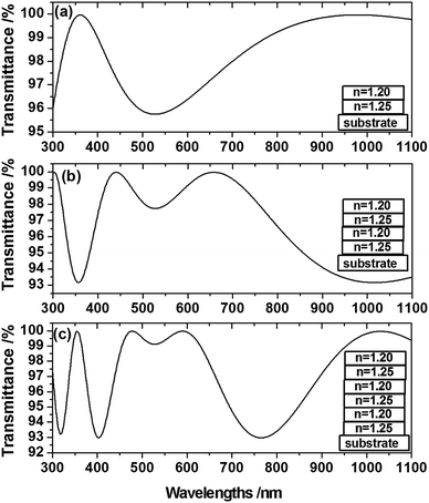 |
| | Fig. 2 Theoretical transmittance spectra of double-layer coating ((a) substrate/1.25/1.20/air), four-layer coating ((b) substrate/1.25/1.20/1.25/1.20/air) and six-layer coating ((c) substrate/1.25/1.20/1.25/1.20/1.25/1.20/air). | |
 |
| | Fig. 3 Theoretical transmittance spectra of six-layer coating with increasing refractive indices of L′ layer from 1.20 to 1.22. | |
 |
| | Fig. 4 Theoretical transmittance spectra of six-layer coating with decreasing refractive indices of L′ layer from 1.20 to 1.17. | |
Table 1 Refractive index of six-layer tri-wavelength AR coatings on fused silica substrate and their transmittance at 1064 nm, 532 nm and 355 nm modeled by TFCalc™ (the central wavelength for these coatings is 528 nm, and the optical thickness is quarter-wave)
| Sample number |
L layer |
L′ layer |
T
355 nm [%] |
T
532 nm [%] |
T
1064 nm [%] |
|
n
1
|
Thickness [nm] |
n
2
|
Thickness [nm] |
| C1 |
1.25 |
105.6 |
1.20 |
110.0 |
100.0 |
99.1 |
99.8 |
| C2 |
1.25 |
105.6 |
1.21 |
109.1 |
99.9 |
98.4 |
99.8 |
| C3 |
1.25 |
105.6 |
1.22 |
108.2 |
99.9 |
97.4 |
99.8 |
| C4 |
1.25 |
105.6 |
1.19 |
110.9 |
100.0 |
99.7 |
99.8 |
| C5 |
1.25 |
105.6 |
1.18 |
111.9 |
99.9 |
100.0 |
99.8 |
| C6 |
1.25 |
105.6 |
1.17 |
112.8 |
100.0 |
100.0 |
99.7 |
| C7 |
1.26 |
104.8 |
1.18 |
111.9 |
100.0 |
100.0 |
99.7 |
| C8 |
1.27 |
103.9 |
1.19 |
110.9 |
99.9 |
100.0 |
99.6 |
| C9 |
1.28 |
103.1 |
1.20 |
110.0 |
99.9 |
100.0 |
99.6 |
|
C10
|
1.29
|
102.3
|
1.21
|
109.1
|
99.8 |
100.0 |
99.5 |
| C11 |
1.24 |
106.5 |
1.16 |
113.8 |
100.0 |
100.0 |
99.7 |
| C12 |
1.23 |
107.3 |
1.15 |
114.8 |
99.9 |
100.0 |
99.6 |
| C13 |
1.22 |
108.2 |
1.15 |
114.8 |
99.9 |
100.0 |
99.7 |
| C14 |
1.22 |
108.2 |
1.14 |
115.8 |
99.9 |
100.0 |
99.6 |
|
C15
|
1.21
|
109.1
|
1.14
|
115.8
|
99.8 |
100.0 |
99.6 |
3.2 Six-layer AR coating from inorganic silica sols
The aim of this work is to prepare TWAR coating for high power laser system. In addition to the excellent transmittance, the TWAR coating must also possess high LIDT and feasible coating technology. All thin films for six-layer TWAR coating for high power laser systems should be the silica or organically modified silica (ORMOSIL) thin films from sol–gel process because they have higher LIDT and easier coating technology.5,27,32 An inorganic silica thin film with refractive index varying from 1.22 to 1.44 were previously reported by mixing acid-catalyzed silica and base-catalyzed silica together in different proportion.19 With the same method, inorganic silica thin films with refractive index varying from 1.21 to 1.34 were 1.21, respectively. As shown in Fig. 5, as the weight ratio of acid-catalyzed silica to base-catalyzed silica is 0.0 and 0.2, the refractive indices of inorganic silica thin films are 1.21 and 1.29, indicating that these two thin films can be used as the L′ layer and L layer of C10 coating. The film thickness of L layer and L′ layer from inorganic silica sols were optimized by varying the dip-coating speed (withdraw rate) to give them with a central wavelength of 528 nm. After this, the six-layer TWAR coating was obtained by alternatively coating the L layer and L′ layer for three times onto fused silica substrate. The transmittance spectrum of the resultant six-layer TWAR coating is shown in Fig. 6 and compared with the theoretical transmittance spectrum of modeled C10. As shown in Fig. 6, the experimental transmittance spectrum is almost in accordance with the modeled spectrum, which indicates that the theoretical design of the six-layer TWAR coating is feasible. However, the transmittance at 355 nm is only 99.1%. In high power laser system, the 355 nm laser is the main laser in the mixed three wavelengths laser. A good TWAR coating should transmit 355 nm laser at nearly 100% (normally more than 99.5%) and transmit the 532 nm and 1064 nm lasers as more as possible. Consequently, the six-layer TWAR coating from inorganic sols cannot meet the requirement of high power laser system.
 |
| | Fig. 5 Effect of weight ratio of acid-catalyzed silica to base-catalyzed silica on the refractive index of inorganic thin films. | |
 |
| | Fig. 6 Water contact angle picture (B) and experimental transmittance spectrum (A) of inorganic six-layer TWAR coating compared with the theoretical transmittance spectrum. | |
3.3 A possible crack problem on the boundary of sol–gel silica multi-layer coating
As discussed in our previous paper, we divided the drying process of sol–gel silica thin film into two different stages.19 At the first stage, a liquid layer of sol converted into an elastic gel-like solid; and at the second stage, the solvent in gel continues to evaporate and finally converted into a porous solid film. During the second stage, the condensation reaction between the hydroxyl groups of adjacent silica particles resulted in shrinkage of the gel network, and the capillary force during evaporation of solvent built up compressive forces around the perimeter of the pores. These two collapsing forces play a very important role in adjustment the microstructure of sol–gel silica thin films. As shown in Fig. 6, the experimental transmittance at 355 nm is smaller than the modeled transmittance. We attributed this phenomenon to a possible crack problem on the interface of multi-layer sol–gel silica coating aroused by also these two collapsing forces. After the second liquid layer being deposited onto the surface of the first layer, the second liquid layer also suffers from the two collapsing forces during the drying process. The shrinkage of network of the second layer and the compressive forces around the perimeter of the pores on the interface produce cracks as shown in Fig. 7. The cracks are about several hundred nanometers in diameter, which would cause light scatter for laser with low wavelength (e.g. 355 nm). This is the possible reason that the experimental transmittance at 355 is smaller than the modeled transmittance. The cross-sectional SEM image was also recorded, and it was shown in the ESI.†
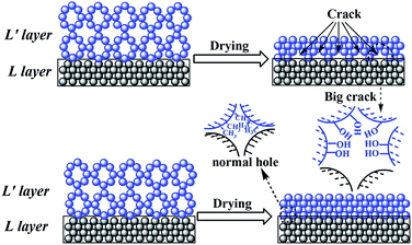 |
| | Fig. 7 Schematic representation of a possible crack problem on the interface of sol–gel silica multi-layer coating. | |
3.4 Six-layer AR coating from ORMOSIL sols
Our previously reported double-layer double-wavelength and double-layer TWAR coatings possess the same transmittance at 355 nm and 532 nm compared to the modeled ones.22,30 It can be found that the top layers of our previous double-layer AR coatings are both the organic–inorganic hybrid films from ORMOSIL sols. The hydrophobic organic groups of organic component can greatly reduce the two collapsing forces because they are un-reactive and have low surface energy, and hence prevent the interface of two layers from generating cracks in large size. Therefore, in the preparation of six-layer AR coating, one of L layer and L′ layer should also be the ORMOSIL thin film to avoid the formation of cracks on the interface of L layer and L′ layer. The ORMOSIL thin films generally have low refractive index of 1.10–1.21.29,33 So, as shown in Table 1, we re-design the six-layer TWAR coatings with film materials of lower refractive indices. As the refractive indices of L layer and L′ layer are 1.21 and 1.14, the modeled transmittance of TWAR coating at 355 nm, 532 nm and 1064 nm is 99.8%, 100.0% and 99.6%.
The L layer and L′ layer can be prepared from the ORMOSIL sols by hybridization of DDS and TEOS in different molar ratio. As shown in Fig. 8, the refractive index of ORMOSIL thin films decreases from 1.21 to 1.13 as the molar ratio of DDS to TEOS increased from 0.0 to 0.6. The refractive index of ORMOSIL thin films is 1.21 and 1.14 when the molar ratio of DDS to TEOS is 0.0 and 0.4. The change in the refractive index is related to the porosity of ORMOSIL thin film which is adjusted by the collapsing forces during the drying process.19,29 Finally, the film thickness of L layer and L′ layer was optimized by varying the dip-coating speed (withdraw rate) to give them with a central wavelength of 528 nm. After this, L layer and L′ layer were deposited onto the fused substrate alternatively for three times to obtain six-layer ORMOSIL TWAR coating.
 |
| | Fig. 8 Effect of molar ratio of DDS to TEOS on the refractive index of ORMOSIL thin films. | |
The transmittance spectrum of the resultant six-layer ORMOSIL TWAR coating compared with the spectra of modelled C15 coating and bare substrate were shown in Fig. 9. The transmittances of the six-layer TWAR coating at 355 nm, 532 nm and 1064 nm are 99.7%, 99.5%, 99.2%, respectively. Compared with the bare substrate, the transmittances of prepared six-layer TWAR coating at 355 nm, 532 nm and 1064 nm increased by 6.9%, 6.1% and 6.1%, respectively. This six-layer TWAR coating from ORMOSIL sols can be included as a good TWAR coating for high power laser system because its transmittance at 355 nm is almost 100% and the transmittance at 532 nm and 1064 nm is also very high.
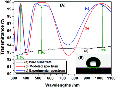 |
| | Fig. 9 Water contact angle picture (B) and experimental transmittance spectrum (A) of ORMOSIL six-layer TWAR coating compared with the theoretical transmittance spectrum. | |
Compared with the inorganic six-layer TWAR coating, the advantages of ORMOSIL six-layer TWAR coating are obvious. First, the transmittance of ORMOSIL TWAR coating at 355 nm is much higher than that of inorganic TWAR coating. L′ layer is deposited by ORMOSIL particles. Second, the ORMOSIL six-layer TWAR coating has better environmental resistance. The water contact angle of inorganic silica thin film is only about 23° (as shown in Fig. 6), while that of L′ layer is 139° (as shown in Fig. 9). The hydrophobic ORMOSIL layers can afford the ORMOSIL six-layer TWAR coating better environmental resistance. This is very important for AR coatings used in high power laser system. Finally, as is well known, the silica and ORMOSIL thin films prepared by the sol–gel process have high LIDT and therefore have been widely used in high power laser systems for several decades.5,30 Therefore, this six-layer TWAR coating prepared by sol–gel process in this work can find great applications in high power laser system.
4. Conclusions
A six-layer tri-wavelength antireflective (TWAR) coating, which has nearly 100% transmittance simultaneously at 1064 nm, 532 nm and 355 nm, was designed with the aid of thin film design software (TFCalc™). Six-layer TWAR coating from inorganic silica sols possessed low transmittance at 355 nm and 532 nm, which was maybe attributed to the collapsing forces during the drying process. Six-layer TWAR coating, which has transmittance of 99.7%, 99.5% and 99.2% at 355 nm, 532 nm and 1064 nm, was successfully obtained from the ORMOSIL sols. Compared with the bare substrate, the transmittances of prepared six-layer TWAR coating at 355 nm, 532 nm and 1064 nm increased by 6.9%, 6.1% and 6.1%, respectively. This six-layer TWAR coating prepared by sol–gel process can find great applications in high power laser system.
Acknowledgements
The authors acknowledge the support of from National Natural Science Foundation of China (61505029, and 61405180) and Natural Science Foundation of Fujian Province of China (2015j05092).
Notes and references
- C. I. Yeo, H. J. Choi, Y. M. Song, S. J. Kang and Y. T. Lee, J. Mater. Chem. A, 2015, 3, 7235 CAS.
- T. Aytug, A. R. Lupini, G. E. Jellison, P. C. Joshi, I. H. Ivanov, T. Liu, P. Wang, R. Menon, R. M. Trejo, E. Lara-curzio, C. R. Hunter, J. T. Simpson, M. P. Paranthaman and D. K. Christen, J. Mater. Chem. C, 2015, 3, 5440 RSC.
- J. F. Tang, Z. L. Tseng, C. Y. Chen, Y. M. Lu and S. Y. Chu, RSC Adv., 2015, 5, 28870 RSC.
- W. Glaubitt and P. Löbmann, J. Eur. Ceram. Soc., 2012, 32, 2995–2999 CrossRef CAS.
-
P. K. Whitman, S. C. Frieders, J. Fair, I. M. Thomas, R. Aboud, C. B. Thorsness and A. K. Burnham, ICF Quarterly Report, 1999, vol. 9, p. 163 Search PubMed.
- D. R. Uhlmann, T. Suratwala, K. Davidson, J. M. Boulton and G. Teowee, J. Non-Cryst. Solids, 1997, 218, 113 CrossRef CAS.
- X. Zhang, Y. Zhang, L. Ye, B. Xiao, L. Yan, H. Lv and B. Jiang, J. Sol-Gel Sci. Technol., 2011, 58, 340 CrossRef CAS.
- X. Li, M. Gross, B. Oreb and J. Shen, J. Phys. Chem. C, 2012, 116, 18367 CAS.
- Q. Zhang, Y. Wei, W. Yang, H. Hui, X. Deng, J. Wang, Q. Xu and J. Shen, RSC Adv., 2015, 5, 4529 RSC.
- X. Zhang, H. Ye, B. Xiao, L. Yan, H. Lv and B. Jiang, J. Phys. Chem. C, 2010, 114, 19979 CAS.
- X. Zhang, B. Xia, H. Ye, Y. Zhang, B. Xiao, L. Yan, H. Lv and B. Jiang, J. Mater. Chem., 2012, 22, 13132 RSC.
- Z. Geng and J. H. He, J. Mater. Chem. A, 2014, 2, 16601–16607 CAS.
- Y. Wang, M. Y. He and R. Y. Chen, J. Mater. Chem. A, 2015, 3, 1609–1618 CAS.
- L. Yao, J. He, Z. Geng and T. Ren, Nanoscale, 2015, 7, 13125–13134 RSC.
- L. Xu, J. He and L. Yao, J. Mater. Chem. A, 2014, 2, 402 CAS.
- F. Chi, L. Yan, H. Lv, C. Wang and X. Yuan, Thin Solid Films, 2011, 519, 2483 CrossRef CAS.
- Y. Xu, L. Zhang, D. Wu, Y. H. Sun, Z. X. Huang, X. D. Jiang, X. F. Wei, Z. H. Li, B. Z. Dong and Z. H. Wu, J. Opt. Soc. Am. B, 2005, 22, 1899 CrossRef CAS.
- I. M. Thomas, Proc. SPIE, 1997, 3136, 215 CrossRef CAS.
- X. Zhang, S. Cai, D. You, L. Yan, H. Lv, X. Yuan and B. Jiang, Adv. Funct. Mater., 2013, 23, 4361 CrossRef CAS.
- P. Belleville and P. Prené, Proc. SPIE, 1999, 3492, 230 CrossRef CAS.
- A. Yildirim, T. Khudiyev, B. Daglar, H. Budunoglu, A. K. Okyay and M. Bayindir, ACS Appl. Mater. Interfaces, 2013, 5, 853 CAS.
- X. Li, J. Gao, L. Xue and Y. Han, Adv. Funct. Mater., 2010, 20, 259 CrossRef CAS.
- X. Li and J. Shen, Thin Solid Films, 2011, 519, 6236 CrossRef CAS.
- J. Cai, J. Ye, S. Chen, X. Zhao, D. Zhang, S. Chen, Y. Ma, S. Jin and L. Qi, Energy Environ. Sci., 2012, 5, 7575 CAS.
- J. Sun, X. Cui, C. Zhang, C. Zhang, R. Ding and Y. Xu, J. Mater. Chem. C, 2015, 3, 7187 RSC.
- Y. Du, L. E. Luna, W. S. Tan, M. F. Rubner and R. E. Cohen, ACS Nano, 2010, 4, 4308 CrossRef CAS PubMed.
- B. Xiao, B. Xia, H. Lv, X. Zhang and B. Jiang, J. Sol-Gel Sci. Technol., 2012, 64, 276 CrossRef CAS.
- R. Ding, X. Cui, C. Zhang, C. Zhang and Y. Xu, J. Mater. Chem. C, 2015, 3, 3219 RSC.
- X. Zhang, W. Su, M. Lin, X. Miao, L. Ye, W. Yang and B. Jiang, J. Sol-Gel Sci. Technol., 2015, 74, 594 CrossRef CAS.
-
H. A. Macleod, Thin-film optical filters, Institute of Physics Publishing, Tucson, 2001, pp. 55–66 Search PubMed.
- H. G. Floch and P. F. Belleville, Proc. SPIE, 1994, 2253, 764 CrossRef CAS.
- I. M. Thomas, Appl. Opt., 1986, 25, 1481 CrossRef CAS PubMed.
- Y. Zhang, C. Zhao, P. Wang, L. Ye, J. Luo and B. Jiang, Chem. Commun., 2014, 50, 13813 RSC.
Footnotes |
| † Electronic supplementary information (ESI) available: The cross-sectional SEM image. See DOI: 10.1039/c6ra04584g |
| ‡ These authors contributed equally to this work. |
|
| This journal is © The Royal Society of Chemistry 2016 |
Click here to see how this site uses Cookies. View our privacy policy here. 


