Eco-friendly photolithography using water-developable pure silk fibroin

Joonhan Parka, Sung-Gyu Leeb, Benedetto Marellic, Myungjae Leed, Taehyung Kima, Hye-Keun Ohb, Heonsu Jeond, Fiorenzo G. Omenettocef and Sunghwan Kim*ag
aDepartment of Energy Systems Research, Ajou University, Suwon 16499, Republic of Korea. E-mail: sunghwankim@ajou.ac.kr
bDepartment of Applied Physics, Hanyang University, Ansan 15588, Republic of Korea
cDepartment of Biomedical Engineering, Tufts University, Medford, MA 02155, USA
dDepartment of Physics and Astronomy, Seoul National University, Seoul 08826, Republic of Korea
eDepartment of Physics, Tufts University, Medford, MA 02155, USA
fDepartment of Electrical and Computer Engineering, Tufts University, Medford, MA 02155, USA
gDepartment of Physics, Ajou University, Suwon 16499, Republic of Korea

Received 19th February 2016 , Accepted 28th March 2016

First published on 14th April 2016


Abstract

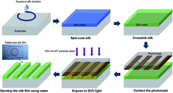
We report that pure silk fibroin can be a green and biofunctional photoresist for deep ultraviolet photolithography. All processes are entirely water-based, from resist solvent to resist removal, and rely on the phototendering effect that decreases the crystallinity of silk fibroin films by DUV exposure. Additionally, the potential decrease in activity of bio-dopants due to high-energy irradiation is irrelevant to our positive-tone lithographic method.


Biological micro- and nanostructures promise many fascinating applications in tissue engineering, drug delivery, and bioelectronics/photonics.1–3 Lithographic top–down approaches have been considered the most important processes for fabricating such structures.4 However, adapting traditional lithography techniques to the biological context often requires indirect strategies using additional resists. This makes lithographic process more complex and involves the use of toxic chemicals that may negatively affect biological matter. Direct patterning of biological materials at the micro- and nanoscale has the potential to enable geometries with eco-friendly and fewer processing steps.5,6 Silk protein, extracted from Bombyx mori cocoons, and its blends with other polymers are attractive for biomedical applications and have recently been reinvented as a biological base material in bio-optics and electronics.7–13 Most recently, silk micro- and nanostructures have been demonstrated by direct writing methods, electron beam lithography (EBL) and photolithography.14–16 In particular, for EBL, pure silk fibroin has been used as a biological resist in all-water-based lithography, starting with a silk aqueous solution and ending with simple development in water, while preserving its biofunctionality throughout the fabrication process.14 The reported silk photoresists, however, have not been pure silk fibroin but composed of chemically modified silk that contained photoinitiators.15,16 This is generally true when patterning proteins with photolithography, where such modifications are necessary to render them photoreactive.

EBL is a maskless patterning technique that generates arbitrary patterns at high resolution. Although EBL offers very highly resolvable patterns and versatility for patterning arbitrary shapes, the technique suffers from some inherent limitations, notably cost and speed.17 In comparison to EBL, photolithography provides cost-effective and high-speed patterning over large areas. Deep ultraviolet (DUV) excimer lasers and liquid immersion techniques have overcome diffraction limitations and the resulting low resolution to yield feature sizes below 50 nm.18

Here, we report entirely water-based positive-tone photolithography on a pure silk fibroin film using an argon fluoride (ArF) excimer laser operating at a wavelength of 193 nm. This wavelength coincides with a region of strong absorption for silk.19 This endogenous feature of silk fibroin enables experiments without chemical modification to the silk solution. Water is the only chemical involved in this lithography process, acting both as a solvent and as a developer. Even removing the silk resist is possible under aqueous salt solutions. Chrome (Cr) mask patterns on fused silica substrates were successfully transferred to the silk films. We explored the area dose and found out that 20 mJ cm−2 corresponds to the optimum dose, which is comparable to those of commercially available DUV resists. Along with this low area dose, the availability of silk at low cost offers a cost-effective resist. Additionally, our positive-tone lithography in which the exposed area is removed after the water development helps to preserve its biofunctionality after the lithography process when the silk resist is biologically activated. When performed in conjunction with the water immersion technique, exposure and development can be performed simultaneously.

Fig. 1 shows a schematic diagram of the photolithography process flow used to generate patterns on silk films. Aqueous silk fibroin solution was spin-coated on glass substrates to form thin silk films with precisely controlled thicknesses. The spin-coated film is initially a self-assembled amorphous polymer and therefore soluble in water.20 We can render the films insoluble in water by inducing the crystallization of silk, called β-sheet formation (see Methods). A coherent laser beam with a wavelength of 193 nm illuminated the silk film through the patterned Cr mask on a fused silica (DUV transparent) substrate and dissociated molecular bonds to render the silk film water-soluble. Then, the exposed area was washed away by rinsing the exposed sample for 1 min in distilled water. As shown in Fig. 1, the washed silk film showed diffracted colors, indicating that the 1D grating patterns of the Cr-mask were transferred to the silk film via DUV photolithography.


image file: c6ra04516b-f1.tif
Fig. 1 Schematic diagrams showing the ArF excimer laser photolithography process to form high-resolution silk fibroin micropatterns. No photoinitiator material was used here, and water was the only chemical involved in this process.

Optical microscopy, scanning electron microscopy (SEM), and atomic force microscopy (AFM) were used to characterize the surface morphology (Fig. 2). The thickness of the spin-coated silk film was 200 nm, and 1D silk gratings with various pitch sizes were successfully generated on the film. As shown in Fig. 2(c) and (d), the obtained minimum periodicity of features was 1 μm, which was also the minimum feature size of the Cr mask. AFM topology showed that the minimum feature had a good vertical profile and a thickness of about 190 nm, similar to the initially spin-coated thickness.


image file: c6ra04516b-f2.tif
Fig. 2 Optical microscopy image in (a) and scanning electron microscopy images in (b) and (c) for the patterned silk fibroin film. Scale bars indicate 50 μm in (a) and (b) and 10 μm in (c). (d) Atomic force microscopy image of the patterned silk shown in (c). The feature was around 190 nm in height and 1 μm in line width.

Fig. 3(a) shows the irradiation sensitivity of the silk photoresist. The DUV laser beam was illuminated on crystallized silk films (200 nm in thickness) with different doses. After the films were developed, AFM was used to obtain the depth of the silk patterns. The dose to fabricate clear patterns was found to be 20 mJ cm−2, which is comparable to commercial photoresists.21,22 Above a dose of 20 mJ cm−2, the depth of the silk patterns decreased. The patterning performance of our photolithography set-up has several limits at the laboratory scale. Even if ArF scanners for the DUV photolithography are commercially available and used by semiconductor manufacturers, the facility cost is too expensive for an academic laboratory. In our photolithography set-up, no optical components, such as lenses or beam expanders, are used for exposure because of cost and accessibility issues. Our previous study on EBL already proved that silk resist could be used to generate 30 nm-diameter features, and therefore the resolution can still be improved under better circumstances. Another limitation is the high peak power of excimer laser pulses, which can exert influence on the silk film even through Cr patterns. Strongly absorbed DUV light during long exposure generates much heat, which then ablates the silk fibroin film.23,24 This can be improved by reducing the power density (expanding the beam size) and using water immersion.


image file: c6ra04516b-f3.tif
Fig. 3 Performance of silk photoresist. (a) Depth of the 1D silk line pattern as a function of dose. At doses over 20 mJ cm−2, the laser beam ablated the silk film even through the chrome layer in the photomask. (b) Etching time dependence of the thickness of the silk resist, other commercial resists, and SiO2. Well established fabrication conditions for SiO2 etching were used for all resists.

An important trait for determining the performance of silk photoresist is drying etching resistance. Chlorine-based gas was used to etch SiO2 in this test, and poly(methyl methacrylate) (PMMA) and ZEP520A, two commercial resists, were used as references. Fig. 3(b) shows that the etch rate of silk fibroin, 9.10 nm s−1, was lower than those of EP520A and PMMA, which were 10.25 nm s−1 and 12.77 nm s−1, respectively. This value is remarkable to prove the practicality of our silk photoresist when considering that ZEP520A has high dry etch resistance and they are almost equivalent to that of positive photoresist generally used.25

Poor adhesion of resist materials to semiconductor substrates decreases the reliability of nanofabrication during post-lithographic processes.26 Adhesion promoters such as hexamethyldisilazane (HMDS) are used to enhance adhesion but lack versatility.27 As an example, HMDS is not an effective adhesion promoter without the formation of siloxane bonds. Therefore, HMDS has limited use when used in conjunction with compound semiconductors. The silk photoresist showed good adhesion to any arbitrary substrate under ultra-sonication treatment while conventional photoresists chipped off (see ESI, Fig. S1 and S2). In addition, to finalize micro/nanofabrication, the resist must be clearly removed by specific chemicals (i.e., the remover). Ionic liquids have been used to successfully dissolve biological macromolecules such as silk fibroin and cellulose.28 The silk films on silicon were immersed in NaCl aqueous solution and then clearly removed after just 1 min, as shown in Fig. S2. Other salt solutions such as lithium salt solution also exhibited the same result, which shows that all lithographic processes using silk can be eco-friendly when performed in all water-based conditions, from solvents for silk fibroin to removers. Additionally, we could fabricate a Cr mask using the lift-off of the Cr-deposited silk fibroin pattern in NaCl aqueous solution (see ESI, Fig. S3).

The use of water as the developer also has further utility for lithographic patterning, where state-of-the-art ArF lithography is performed in immersion by filling the space between the projection lens and the sample with water to increase the resolution. The use of a water-developable silk resist opens the possibility to perform in situ patterning during exposure (see ESI, Fig. S4). To demonstrate the principle without resorting to state-of-the-art facilities, a thin air gap was introduced between the sample and the photomask and then filled with water from one side of the rectangular sample. After optimal exposure with a dose of 20 mJ cm−2 and nitrogen gas blowing, clearly diffracted colors could be seen from the silk film, and AFM images revealed that the aspect ratios matched the results of free-space exposure. This experiment validated the feasibility of a water immersion approach and the possibility of using this approach as a useful direct writing method similar to focused ion beam writing.

The transition between the amorphous and crystalline structures of silk correlates with water solubility and is the basis of the water-developable silk resist. Fourier-transform infrared (FTIR) spectroscopy was used to verify the mechanism governing the transition (Fig. 4). The amide I (1600–1700 cm−1) and amide II (1450–1600 cm−1) regions were selected to monitor the formation of β-sheets.29 The absorption peak centered at 1641 cm−1 indicates the typical random coil organization of the amorphous protein while the peak at 1626 cm−1 indicates the β-sheet conformation of the cross-linked protein. The crystallized silk film exhibited a decrease in absorption at 1641 cm−1 when compared to its amorphous counterpart. The exposed crystalline silk displayed a decrease in the absorption peak at 1626 cm−1 in the FTIR spectrum with the irradiation dose. DUV light with a wavelength lower than 280 nm can cause photo-oxidation of aromatic amino acids, such as tyrosine, tryptophan, and phenylalanine, that exist in the silk fibroin.30 This induces peptide fission initially at the weaker C–N bond, which accounts for a reduction in the degree of silk crystallinity and hence silk phototendering (loss of strength). These results are consistent with the mechanism of our positive-tone photolithography.


image file: c6ra04516b-f4.tif
Fig. 4 Effect of 193 nm laser exposure on silk polymeric properties. The plot shows the FTIR microscopy spectra of amorphous, crystalline, and laser-beam-exposed silk fibroin. The ratio of the absorbance at 1641 cm−1 to that at 1626 cm−1 in the amide I region indicates the crystallinity of the silk film.

Photolithographic writing methods provide versatile and useful ways to obtain micro/nanostructured bio-templates, and silk fibroin is a remarkable polymer matrix to preserve the activity of bio-dopants such as enzymes and fluorescent protein, even under harsh environmental conditions.31 However, with bio-functionalized silk micro/nano-templates, DUV irradiation to crosslink the polymeric network in negative-tone lithography, as shown by other reported results, may attenuate the biofunction of the bio-dopant because the high-energy DUV photons can directly damage the electronic system of the biomolecules and photoproducts can also modify bio-dopants.32 Therefore, our positive-tone lithography scheme, which generates a pattern by removing the exposed region, is free from the inherent damage to bio-dopants caused by high-energy irradiation. Silk films doped with horseradish peroxidase (HRP) were prepared for use as photoresists. After exposure with different dosages, the exposed areas were further exposed to 3,3′,5,5′-tetramethylbenzidine (TMB) solution to test the activity of the HRP stabilized within the silk resists. As shown in Fig. 5, colorimetric reactions, indicating the activity of the HRP, are seen in the control case (no exposure) for the amorphous silk films. The silk films were not washed with water to test damage by exposure only. The photographs illustrate that even very weak exposure could impair the HRP in silk films. As increasing the dose, the blue color reaction was being weaken that could be read directly on absorption at the wavelength of 650 nm. The doses of 10 and 20 mJ cm−2 were too weak to ablate the silk films, which is indirect evidence that the positive-tone lithographic patterning is a way to eliminate potential damage to bio-dopants caused by high-energy irradiation during fabrication.


image file: c6ra04516b-f5.tif
Fig. 5 Deactivation of the biofunctionalized silk film by 193 nm laser exposure. (a) Absorption spectra for colorimetric reactions of HRPs doped in the silk films to TMB solution. (b–d) Corresponding photographs of the HRP-TMB reactions. As the dose increased, the blue color weakened and the absorption at 650 nm decreased.

Conclusions

We have shown that a pure silk fibroin film can be applied as a positive-tone photoresist for ArF excimer laser lithography. The process is entirely water-based (from solvent to remover) and offers a relatively simple way to generate microscale patterns. The resolution of patterns can still be reduced to the nanoscale when commercial and expensive ArF scanners can be adopted for patterning. Additionally, water-immersion, a conventional method to increase the numerical aperture of ArF scanners, may enable direct patterning of silk film. Silk resist shows good etching resistance and hence is useful as a soft mask. FTIR analysis indicates that our scheme is based on peptide fission by DUV-induced phototendering. The facile doping of silk solutions enables a wide range of biofunctionalization of silk resist. We show that positive-tone lithography, in which the exposed area is removed, is the best way to preserve the activity of biofunctions in the silk film because UV irradiation deactivates the bio-dopants. Along with green cleanroom processing, the versatile material traits of silk fibroin are ideal for lithography-based fabrication at the confluence of micro/nanoscale forms and biological functions.

Acknowledgements

This work was supported by the National Research Foundation (NRF) of Korea grants funded by the Korea government (2014R1A1A1008080, 2014K2A1B8048519, 2009-0082580). S. K. was also supported by the TJ Park Science Fellowship of the POSCO TJ Park Foundation.

References

  1. A. D. Pris, Y. Utturkar, C. Surman, W. G. Morris, A. Vert, S. Zalyubovskiy, T. Deng, H. T. Ghiradella and R. A. Potyraillo, Nat. Photonics, 2012, 6, 195 CrossRef CAS .
  2. M. P. Lutolf and J. A. Hubbel, Nature Biotechnology, 2005, 23, 47 CrossRef CAS PubMed .
  3. J.-W. Yoo, D. J. Irvine, D. E. Discher and S. Mitragotri, Nat. Rev. Drug Discovery, 2011, 10, 521 CrossRef CAS PubMed .
  4. R. Kargl, T. Mohan, S. Köstler, S. Spirk, A. Doliška, K. Stana-Kleinschek and V. Ribitsch, Adv. Funct. Mater., 2013, 23, 308 CrossRef CAS .
  5. E. Bat, J. Lee, U. Y. Lau and H. D. Maynard, Nat. Commun., 2015, 6, 6654 CrossRef CAS PubMed .
  6. C. J. Lo, T. Aref and A. Bezryadin, Nanotechnology, 2006, 17, 3264 CrossRef CAS .
  7. F. G. Omenetto and D. L. Kaplan, Nat. Photonics, 2008, 2, 641 CrossRef CAS .
  8. S.-W. Hwang, H. Tao, D.-H. Kim, H. Y. Cheng, J.-K. Song, E. Rill, M. A. Brenckle, B. Panilaitis, S. M. Won, Y.-S. Kim, Y. M. Song, K. J. Yu, A. Ameen, R. Li, Y. Su, M. Yang, D. L. Kaplan, M. R. Zakin, M. J. Slepian, Y. Huang, F. G. Omenetto and J. A. Rogers, Science, 2012, 337, 1640 CrossRef CAS PubMed .
  9. J. Park, Y. Choi, M. Lee, H. Jeon and S. Kim, Nanoscale, 2015, 7, 426 RSC .
  10. S. Kim, A. N. Mitropoulos, J. D. Spitzberg, H. Tao, D. L. Kaplan and F. G. Omenetto, Nat. Photonics, 2012, 6, 818 CrossRef CAS .
  11. H. Tao, J. J. Amsden, A. C. Strikwerda, K. Fan, D. L. Kaplan, X. Zhang, R. D. Averitt and F. G. Omenetto, Adv. Mater., 2010, 22, 3527 CrossRef CAS PubMed .
  12. M. Lee, H. Jeon and S. Kim, Nano Lett., 2015, 15, 3358 CrossRef CAS PubMed .
  13. H. Kwon and S. Kim, ACS Photonics, 2015, 2, 1675 CrossRef CAS .
  14. S. Kim, B. Marelli, M. A. Brenckle, A. N. Mitropoulos, E.-S. Gil, K. Tsioris, H. Tao, D. L. Kaplan and F. G. Omenetto, Nat. Nanotechnol., 2014, 9, 306 CrossRef CAS PubMed .
  15. N. E. Kurland, T. Dey, S. C. Kundu and V. K. Yadavalli, Adv. Mater., 2013, 25, 6207 CrossRef CAS PubMed .
  16. N. E. Kurland, T. Dey, C. Wang, S. C. Kundu and V. K. Yadavalli, Adv. Mater., 2014, 26, 4431 CrossRef CAS PubMed .
  17. A. A. Tseng, K. Chen, C. D. Chen and K. J. Ma, IEEE Trans. Electron. Packag. Manuf., 2003, 26, 141 CrossRef CAS .
  18. J. A. Hoffnagle, W. D. Hinsberg, M. Sanchez and F. A. Houle, J. Vac. Sci. Technol., B: Microelectron. Nanometer Struct.--Process., Meas., Phenom., 1999, 17, 3306 CrossRef CAS .
  19. A. Sionkowska and A. Planecka, Polym. Degrad. Stab., 2011, 96, 523 CrossRef CAS .
  20. M. A. Brenckle, H. Tao, S. Kim, M. Paquette, D. L. Kaplan and F. G. Omenetto, Adv. Mater., 2013, 25, 2409 CrossRef CAS PubMed .
  21. T. G. Oyama, A. Oshima, M. Washio and S. Tagawa, AIP Adv., 2011, 1, 042153 CrossRef .
  22. T. F. Deutsch and M. W. Geis, J. Appl. Phys., 1983, 54, 7201 CrossRef CAS .
  23. Y.-M. Huang, M. Uppalapati, W. O. Hancock and T. N. Jackson, Lab Chip, 2008, 8, 1745 RSC .
  24. M. B. Applegate, J. Coburn, B. P. Partlow, J. E. Moreau, J. P. Mondia, B. Marelli, D. L. Kaplan and F. G. Omenetto, Proc. Natl. Acad. Sci. U. S. A., 2015, 112, 12052 CrossRef CAS PubMed .
  25. D. M. Tanenbaum, C. W. Lo, M. Isaacson, H. G. Craighead, M. J. Rooks, K. Y. Lee, W. S. Huang and T. H. P. Chang, J. Vac. Sci. Technol., B: Microelectron. Nanometer Struct.--Process., Meas., Phenom., 1996, 14, 3829 CrossRef CAS .
  26. A. Singh, J. Jayaram, M. Madou and S. Akbar, J. Electrochem. Soc., 2002, 149, E78 CrossRef CAS .
  27. J. N. Helbert and N. Saha, J. Adhes. Sci. Technol., 1991, 5, 905 CrossRef CAS .
  28. D. M. Phillips, L. F. Drummy, D. G. Conrady, D. M. Fox, R. R. Naik, M. O. Stone, P. C. Trulove, H. C. De Long and R. A. Mantz, J. Am. Chem. Soc., 2004, 126, 14350 CrossRef CAS PubMed .
  29. X. Hu, K. Shmelev, L. Sun, E.-S. Gil, S.-H. Park, P. Cebe and D. L. Kaplan, Biomacromolecules, 2011, 12, 1686 CrossRef CAS PubMed .
  30. J. Shao, J. Zheng, J. Liu and C. M. Carr, J. Appl. Polym. Sci., 2005, 96, 1999 CrossRef CAS .
  31. E. M. Pritchard, P. B. Dennis, F. G. Omenetto, R. R. Naik and D. L. Kaplan, Biopolymers, 2012, 97, 479 CrossRef CAS PubMed .
  32. A. R. Blaustein, P. D. Hoffman, D. G. Hokit, J. M. Klesecker, S. C. Walls and J. B. Hays, Proc. Natl. Acad. Sci. U. S. A., 1994, 91, 1791 CrossRef CAS .

Footnote

Electronic supplementary information (ESI) available. See DOI: 10.1039/c6ra04516b

This journal is © The Royal Society of Chemistry 2016