Piezo-Hall effect in single crystal p-type 3C–SiC(100) thin film grown by low pressure chemical vapor deposition

Afzaal Qamar*a, H.-P. Phana, Toan Dinha, Li Wanga, Sima Dimitrijevab and Dzung Viet Daoab
aQueensland Micro- and Nanotechnology Centre, Griffith University, Queensland, Australia. E-mail: afzaal.qamar@griffithuni.edu.au
bSchool of Engineering, Griffith University, Queensland, Australia

Received 19th February 2016 , Accepted 14th March 2016

First published on 16th March 2016


Abstract

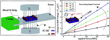
This article reports the first results on piezo-Hall effect in single crystal p-type 3C–SiC(100) Hall devices. Single crystal p-type 3C–SiC(100) was grown by low pressure chemical vapor deposition, and Hall devices were fabricated using the conventional photolithography and dry etching processes. An experimental setup capable of applying stress during Hall-effect measurements was designed to measure the piezo-Hall effect. The piezo-Hall effect is quantified by directly observing the variation in magnetic field sensitivity of the Hall devices upon an applied stress. The piezo-Hall coefficient P12 characterized by these measurements is found to be 6.4 × 10⁻¹¹ Pa−1.


The piezo-Hall effect in silicon (Si) has been widely studied over the past few decades and it has been used to compensate the magnetic field sensitivity drifts in Hall devices. The drift in magnetic field sensitivity of Hall devices results from several fabrication and post fabrication factors, with stresses introduced by encapsulation being the most important factor.1–7 These stress variations can seriously affect the magnetic field sensing measurements and signal processing on chip by affecting the design parameters, temperature behavior and offset voltage.1 The piezoresistive effect and piezo-Hall effect both are important for magnetic field sensors and a large number of studies on Si can be found in the literature.1–7 However, the low energy band gap of Si limits its use for high temperature applications. Silicon carbide on the other hand has a wide band gap, high thermal conductivity, low thermal-expansion coefficient, better mechanical strength, good thermal-shock resistance and chemical stability, which make it a promising material for applications in harsh environments.8–10 SiC can be found in various polytypes, including 4H–SiC, 6H–SiC, and 3C–SiC. The compatibility of 3C–SiC with the existing process of micro-electro-mechanical systems (MEMS) makes it a favorable polytype over other polytypes. Its hetero-epitaxial growth capability over Si substrates of different crystal orientations, e.g., (100), (110) or (111),11–13 make it a material of choice for harsh environment applications.

Various polytypes of SiC have been explored for piezoresistive effects and it has been found that the SiC is a promising material for strain or stress sensing applications in harsh environments.14–20 Phan et al.21–24 presented a comprehensive study on the piezoresistive effect in single crystal p-type 3C–SiC grown by low pressure chemical vapor deposition (LPCVD). A gauge factor (GF) upto 30 has been reported in p-type 3C–SiC which shows its potential for stress sensing applications. Fundamental piezoresistive coefficients of p-type 3C–SiC have also been reported. It has been found that the piezoresistive effect depends upon the crystal orientation and it can also be affected by the defect density in the crystal.21–24 Piezojunction effects in p-3C–SiC/p-Si and n-3C–SiC/p-Si heterojunctions has also been reported, which shows that the applied stress can vary the current–voltage characteristics of the heterojunctions.25,26 The pseudo-Hall effect (variation of offset voltage of Hall devices with applied stress without magnetic field) in LPCVD grown p-type 3C–SiC(100) and p-type 3C–SiC(111) Hall devices has been reported.27–30 The offset voltage of the Hall devices varies significantly even without application of the magnetic field. This pseudo-Hall effect also depends upon the device geometry and crystal orientation and it can be minimized for certain crystallographic orientations. The pseudo-Hall effect is also important for magnetic field sensors because this effect must be subtracted in order to get the real magnetic field sensitivity of the Hall device.

To the best of our knowledge, there has been no report on the piezo-Hall effect in single crystal p-type 3C–SiC(100) Hall devices. Therefore, this paper aims to investigate the piezo-Hall effect in single crystal p-type 3C–SiC(100) Hall devices grown by LPCVD. The results achieved in this study can be used to understand the stress related drifts in the magnetic field sensitivity of Hall devices.

The growth of 3C–SiC thin film on Si(100) was performed using the LPCVD process at low temperature (1000 °C) utilizing SiH4 and C3H6 precursors as the source of Si and C atoms.31 Alternating supply epitaxy (ASE) was employed to grow the single crystal, 3C–SiC(100), on Si(100). The grown film was in situ doped with trimethyaluminium (TMAl) as a source of Al (p-type dopant).31,32 The thickness of the grown film (300 nm) was measured by using a spectrophotometer Nanospec AFT 210. Physical characterization of the thin film was carried out by X-ray diffraction (XRD) and selected area electron diffraction (SAED) techniques. Fig. 1(a) shows the XRD pattern of the grown film in conventional θ–2θ scan mode. It can be confirmed from Fig. 1(a) that the single crystal 3C–SiC(100) was grown on Si(100). The inset of Fig. 1(a) shows the rocking curve of the 3C–SiC(100) peak and the observed FWHM value is 0.80°. Fig. 1(b) shows the SAED pattern of the grown thin film which confirms it is single crystalline. Atomic force microscopy (AFM) was used to measure the roughness of the grown thin film (Fig. 1(c)) which showed a root mean square (RMS) roughness of 20 ± 0.5 nm for a scan area of 5 × 5 μm. The electrical properties of the grown film were characterized using Hall effect measurements. The carrier concentration of p-type single crystalline 3C–SiC was found to be 8 × 1018 cm−3, while the carrier concentration of the Si substrate was 5 × 1014 cm−3. The resistivity of the SiC thin film was measured to be 0.44 Ω cm and the hole mobility of the single crystalline 3C–SiC thin film was found to be 1.88 cm2 V−1 s−1.


image file: c6ra04501d-f1.tif
Fig. 1 (a) The XRD pattern of 3C–SiC(100) grown on Si(100), the inset shows the rocking curve; (b) SAED image of the thin film; (c) AFM image of 5 × 5 μm area of grown thin film.

Rectangular Hall devices (700 × 300 μm) were fabricated by conventional photolithography and dry etch processes (Fig. 2(a)) to investigate the stress-induced piezo-Hall effect. The sputtering process was used to deposit aluminium for ohmic contacts to the device. After fabrication of the device, gold wire bonding was used for input and output signals from the device. The wafer was diced into strips with dimensions of 60 × 9 × 0.625 mm to apply stress by the bending beam method. A dedicated experimental setup capable of applying magnetic field and mechanical stress simultaneously was designed to measure the piezo-Hall effect as shown in Fig. 2(b). Two permanent magnets having a field strength of 0.67 T with opposite poles were fixed in an aluminium box, leaving a space to insert the sample in the magnetic field between them. A cantilever was designed within the box in which one end of the beam with the devices was fixed, while the other end was bent by a known force in the presence of a magnetic field. The bi-layer model has been used to calculate the stress-induced to 3C–SiC Hall devices on Si beam. The method to numerically calculate the stress-induced into the 3C–SiC layer on Si strip is reported elsewhere.23 The applied stress induced in the SiC layer was in the range of 0 to 343 MPa. The ohmic contacts were confirmed by IV measurements as depicted in Fig. 2(c). Horizontal and vertical current leakage from 3C–SiC(100) through to the Si substrate (Fig. 2(c)) were also investigated to confirm that the leakage does not contribute to the measurements. The Al contacts showed good ohmic behavior and the total leakage of current was less than 0.5% of the total device current. A large valence band offset between p-Si and p-3C–SiC (1.7 eV) prevents the leakage current going through the SiC/Si junction.25,26 A schematic presentation of the Hall effect in the fabricated device is shown in Fig. 2(d). The input current is applied between terminals 1 and 2 and the Hall voltage is observed at terminals 3 and 4. The contacts for current flow are strip-like in order to have the uniform current flow in the structure and the uniform effect of stress on the current flow. If the contacts for current are point-like, the current lines will bend and introduce a small source of error in the measurements. In the presence of a constant magnetic field, B, when stress is applied to the device at constant input current, the Hall voltage across terminals 3 and 4 will change with the increase of applied stress, which is the piezo-Hall effect.


image file: c6ra04501d-f2.tif
Fig. 2 (a) Microscopic image of the fabricated rectangular Hall device; (b) experimental setup for piezo-Hall measurements; (c) ohmic behavior of the contacts and leakage currents; (d) schematic presentation of the Hall effect in the fabricated device.

For a cubic crystal such as 3C–SiC, the magnetic field B, current density J and the electric field vector E can be represented by the following equation:1

 
E = ρJ − (RB) × J (1)
where the coefficient ρ is resistivity and R is the Hall coefficient. The first term in eqn (1) describes the resistance while the second term describes the Hall effect. The coefficients ρ and R are generally second rank tensors, which reduce to simple scalars ρ0 and R0 in an unstressed case. The most general linear dependence of Hall coefficient R on the applied stress σ can be represented by the following equation:1
 
image file: c6ra04501d-t1.tif(2)
where Pijkl is the piezo-Hall coefficient and σkl is the stress component. The directional indices i, j, k, and l can take values 1, 2, 3. The magnetic field sensitivity of the Hall device can be described by the following equation:1
 
S = VH/I/B = RH(G/t)[VA−1T−1] (3)
where VH is the Hall voltage observed at terminals 3 and 4, I is the current flowing through terminals 1 and 2 as shown in Fig. 2(d) and B is the magnetic field. RH is the Hall coefficient, G is the geometrical correction factor and t is the thickness of the 3C–SiC thin film. Fig. 3 shows the variation of Hall voltage of the rectangular Hall plate when the stress is varied from 0 to 343 MPa. It can be observed from Fig. 3 that at a fixed value of current in the [100] direction, when stress is applied in the [100] direction, the Hall voltage increases linearly with the increase of applied stress. This increase of the Hall voltage at terminals 3 and 4 leads to a change in sensitivity of the Hall plate, i.e., the piezo-Hall effect. As the value of the applied current is increased the corresponding Hall voltage is also increased and its stress dependency shows a smooth linear behavior. The offset voltage of the device, Voff (the voltage at terminals 3 and 4 in the absence of the magnetic field B), was also calculated and subtracted from the voltage measured at terminals 3 and 4 in order to get the true Hall voltage. Similarly, Voff also changes with stress and its variation with stress is also subtracted from the voltage measured at terminals 3 and 4 in order to get the true piezo-Hall effect which is different from the pseudo-Hall effect.27–29


image file: c6ra04501d-f3.tif
Fig. 3 Dependence of change in Hall voltage on applied stress at different input currents to the Hall device. The directions of applied magnetic field B, input current and applied stress are also shown.

Fig. 4 shows the variation of change in Hall voltage on the applied stress when the magnetic field B was reversed. It can be observed from Fig. 4 that the change in Hall voltage with applied stress showed reversed behavior as compared to the previous case. The Hall voltage VH showed a linear decrease with the increase of applied stress, which verified the Hall effect measurements. The change in VH is proportional to the change in applied current at terminals 1 and 2. The change in the sensitivity of Hall plates was measured by calculating the change in Hall voltage while ignoring the small variations in the dimensions of the Hall plate and very small variations in Hall angle due to deflection of the beam. Fig. 5 shows the dependence of magnetic field sensitivity on the applied stress and the relative change in the magnetic field sensitivity. It can be observed that the magnetic field sensitivity linearly depends upon the applied stress and the maximum relative change in sensitivity of the device is 2.18% at a maximum stress of 343 MPa.


image file: c6ra04501d-f4.tif
Fig. 4 Dependence of change in Hall voltage on applied stress at different input currents with magnetic field B reversed. The directions of magnetic field B, input current and applied stress are also shown.

image file: c6ra04501d-f5.tif
Fig. 5 The dependence of magnetic field sensitivity and the relative magnetic field sensitivity on the applied stress.

When the stress is always applied within the plane of the Hall plate, i.e., perpendicular to the magnetic field B, piezo-Hall coefficients P12 can be determined.1 In the present experiment when B‖[001], I‖[100], the Hall field EH‖[010] and the uni-axial stress is σ‖[100], eqn (2) is reduced to the following relation:

 
image file: c6ra04501d-t2.tif(4)
where P12 is the piezo-Hall coefficient and σ[100] is the stress parallel to the [100] direction. The relation between change in magnetic field sensitivity and the piezo-Hall coefficient P12 is derived from eqn (3) and (4) and is given as:
 
image file: c6ra04501d-t3.tif(5)
where ΔS is the change in magnetic field sensitivity due to the applied stress. The piezo-Hall coefficient P12 calculated from the above relation was found to be 6.4 × 10⁻¹¹ Pa−1.

The piezo-Hall effect in LPCVD grown single crystal p-type 3C–SiC(100) thin film has been observed. After the fabrication of 3C–SiC(100) Hall plates, a dedicated setup capable of applying magnetic field and stress simultaneously has been designed to observe the piezo-Hall effect. Variations in Hall voltage with the application of applied stress have been used to record the variations in magnetic field sensitivities which is then used to calculate the piezo-Hall coefficient P12 having a value of 6.4 × 10⁻¹¹ Pa−1. Variations upto 2.18% in relative magnetic field sensitivity of the fabricated Hall plates were easily observed with the designed setup at the maximum applied stress of 343 MPa. The results of this study can be utilized to compensate for the piezo-Hall effect in the design of p-type 3C–SiC(100) Hall sensors.

Acknowledgements

This work was performed in part at the Queensland node of the Australian National Fabrication Facility, a company established under the National Collaborative Research Infrastructure Strategy to provide nano and micro-fabrication facilities for Australia’s researchers. This work has been partially supported by the Griffith University’s New Researcher Grants.

References

  1. B. Halg, J. Appl. Phys., 1988, 64, 276–282 CrossRef.
  2. S. Huber, C. Schott and O. Paul, IEEE Sens. J., 2013, 13, 2890–2898 CrossRef.
  3. H. Husstedt, U. Ausserlechner and M. Kaltenbacher, IEEE Sens. J., 2011, 11, 2993–3000 CrossRef CAS.
  4. A. Nathan and T. Manku, Appl. Phys. Lett., 1993, 62, 2947–2949 CrossRef CAS.
  5. J. M. Cesaretti, W. P. Taylor, G. Monreal and O. Brand, IEEE Trans. Magn., 2009, 45, 4482–4485 CrossRef CAS.
  6. R. Steiner, C. Maier, M. Mayer, S. Bellekom, H. Baltes and J. Mems, IEEE, 1999, 8, 466–472 Search PubMed.
  7. D. Manic, J. Petr and R. Popovic, Microelectron. Reliab., 2001, 41, 767–771 CrossRef.
  8. P. M. Sarro, Sens. Actuators, A, 2000, 82, 210–2018 CrossRef CAS.
  9. G. yi Li, J. Ma, G. Peng, W. Chen, Z. yong Chu, Y. he Li, T. jiao Hu and X. dong Li, ACS Appl. Mater. Interfaces, 2014, 6, 22673–22679 Search PubMed.
  10. M. Mehregany, C. A. Zorman, N. Rajan and C. H. Wu, Proc. IEEE, 1998, 86, 1594 CrossRef CAS.
  11. J. S. Shor, D. Goldstein and A. D. Kurtz, IEEE Trans. Electron Devices, 1993, 40, 1093 CrossRef CAS.
  12. F. L. Via, M. Camarda and A. L. Magna, Appl. Phys. Rev., 2014, 1, 031301 Search PubMed.
  13. S. Roy, C. Jacob and S. Basu, IEEE Trans. Electron Devices, 2003, 94, 298 CAS.
  14. J. Casady and R. Johnson, Solid-State Electron., 1996, 39, 1409–1422 CrossRef.
  15. J. Bi, G. Wei, L. Wang, F. Gao, J. Zheng, B. Tang and W. Yang, J. Mater. Chem. C, 2013, 1, 4514 RSC.
  16. F. Gao, J. Zheng, M. Wang, G. Wei and W. Yang, Chem. Commun., 2011, 47, 11993 RSC.
  17. R. Shao, K. Zheng, Y. Zhang, Y. Li, Z. Zhang and X. Han, Appl. Phys. Lett., 2012, 101, 233109 CrossRef.
  18. T. Akiyama, D. Briand and N. F. Rooij, J. Micromech. Microeng., 2012, 22, 085034 CrossRef.
  19. R. S. Okojie, A. A. Ned, A. D. Kurtz and W. N. Carr, IEEE Trans. Electron Devices, 1998, 45, 785 CrossRef CAS.
  20. R. Okojie, D. Lukco, V. Nguyen and E. Savrun, IEEE Electron Device Lett., 2015, 36, 174 CrossRef.
  21. H. P. Phan, P. Tanner, D. V. Dao, L. Wang, N. T. Nguyen, Y. Zhu and S. Dimitrijev, IEEE Electron Device Lett., 2014, 35, 399–401 CrossRef CAS.
  22. H. P. Phan, D. V. Dao, P. Tanner, N. T. Nguyen, L. Wang, Y. Zhu and S. Dimitrijev, Appl. Phys. Lett., 2014, 104, 111905 CrossRef.
  23. H. P. Phan, D. V. Dao, P. Tanner, N. T. Nguyen, J. S. Han, S. Dimitrijev, G. Walker, L. Wang and Y. Zhu, J. Matter. Chem. C, 2014, 2, 7176–7179 RSC.
  24. H. P. Phan, D. V. Dao, L. Wang, T. Dinh, N.-T. Nguyen, A. Qamar, P. Tanner, S. Dimitrijev and Y. Zhu, J. Matter. Chem. C, 2015, 3, 1172–1176 RSC.
  25. A. Qamar, P. Tanner, D. V. Dao, H.-P. Phan and T. Dinh, IEEE Electron Device Lett., 2014, 35, 1293–1295 CrossRef.
  26. A. Qamar, D. V. Dao, P. Tanner, H.-P. Phan, T. Dinh and S. Dimitrijev, Appl. Phys. Express, 2015, 8, 061302 CrossRef.
  27. A. Qamar, H.-P. Phan, D. Dao, P. Tanner, T. Dinh, L. Wang and S. Dimitrijev, IEEE Electron Device Lett., 2015, 36, 708–710 CrossRef CAS.
  28. A. Qamar, P. Hoang-Phuong, J. Han, P. Tanner, T. Dinh, L. Wang, D. V. Dao and S. Dimitrijev, J. Mater. Chem. C, 2015, 3, 8804–8809 RSC.
  29. A. Qamar, P. Hoang-Phuong, J. Han, P. Tanner, T. Dinh, L. Wang, D. V. Dao and S. Dimitrijev, J. Mater. Chem. C, 2015, 3, 8804–8809 RSC.
  30. P. Hoang-Phuong, A. Qamar, D. V. Dao, T. Dinh, L. Wang, J. Han, P. Tanner, S. Dimitrijev and N.-T. Nguyen, RSC Adv., 2015, 5, 56377–56381 RSC.
  31. L. Wang, A. Iacopi, S. Dimitrijev, G. Walker, A. Fernandes, L. Hold and J. Chaia, Thin Solid Films, 2014, 564, 39–44 CrossRef CAS.
  32. L. Wang, S. Dimitrijev, J. Han, P. Tanner, A. Lacopi and L. Hold, J. Cryst. Growth, 2011, 329, 67–70 CrossRef CAS.

This journal is © The Royal Society of Chemistry 2016
Click here to see how this site uses Cookies. View our privacy policy here.