
Fluorescence-enhancing plasmonic silver nanostructures using azopolymer lithography†
Ville Pale*,
Christoffer Kauppinen,
Jorma Selin,
Markku Sopanen and
Ilkka Tittonen
Department of Micro and Nanosciences, Aalto University, P.O. Box 13500, FI-00076 Aalto, Finland. E-mail: ville.pale@aalto.fi; Fax: +35 8207227012; Tel: +35 8405437564
First published on 4th May 2016
Abstract
The performance of fluorescence-based measurement techniques is fundamentally limited by the intrinsic quantum yield of a fluorophore. Radiative decay engineering using metallic nanostructures has significant potential to improve the fluorescence emission of a fluorophore. Especially, periodic arrays of metallic nanostructures have the advantage of exhibiting a strong optical response, which is beneficial for improving sensitivity in surface enhanced spectroscopic techniques. In this work, we present a cost-effective and large-scale fabrication scheme for creating periodic plasmonic nanoparticle arrays for fluorescence enhancement. The fabrication process uses an azopolymer mask that forms a two-dimensional surface relief grating when illuminated with two orthogonal exposures, which can directly be used as a soft etching mask to define the nanoparticle array. This approach allows the creation of periodic arrays of symmetrical metallic nanostructures that exhibit good long-range order. Furthermore, the dimensions of the array and the structures can be tuned by changing the exposure or process parameters. The plasmonic behaviour of the fabricated structures was studied both experimentally and by numerical simulations. The fluorescence enhancement performance for the blue and green wavelength regions was verified by using Rhodamine 6G and Cascade Blue as fluorophores. A significant 14-fold fluorescence intensity increase for Rhodamine 6G was observed, whereas the fluorescence intensity for Cascade Blue was roughly doubled. In addition, time-resolved measurements displayed a shortening of the fluorescence lifetime for both of the fluorophores when deposited on the nanoparticle grating. We expect that this approach could be advantageous for other application areas of plasmonics, such as SERS or sensing.
1 Introduction
The optical detection of fluorescent molecules is a common experimental method applied in the various fields of biotechnology,1 medical research2 and clinical chemistry.3 The fundamental processes in fluorescence that affect emission, such as resonance energy transfer, quenching and environmental effects, are well understood.4–7 The majority of fluorescence-based techniques directly rely on the detection of fluorescence from extrinsic fluorophores that are used to label macromolecules. Moreover, inexpensive, label-free fluorescence detection schemes are emerging to facilitate the problems associated with the growing complexity of labelling macro- and biomolecules.8 In both approaches, the attainable detection sensitivity is limited by the intrinsic optical properties of the emissive moiety.During the past few years, radiative decay engineering using plasmonic metallic nanostructures has dramatically improved detection sensitivity even down to the single molecule level9 and brought forth the widespread utilization of various surface enhanced spectroscopy techniques, such as metal enhanced fluorescence (MEF)10,11 and surface enhanced Raman scattering (SERS).12 The sensitivity enhancement originates from localized surface plasmon resonance (LSPR) taking place on a metallic nanostructure that can concentrate the incident light on the nanometer scale and increase the local electromagnetic field strength by several orders of magnitude.13
Placing fluorophores in the vicinity of a nanostructure can either result in quenching or enhancement of fluorescence depending on the fluorophore–structure distance.14 An increase in fluorescence emission is usually also accompanied by a decrease in excited-state lifetime.8,15 The increase in the fluorescence intensity consists of a combination of processes that include enhanced absorption of the fluorophore, changes in the radiative decay pathways and improved fluorescence emission to the far field.15 In general, the factors that influence the optical properties of a plasmonic nanostructure are the shape, size, dielectric environment and material of the structure.16 From a material selection point of view, noble metals, such as gold and silver, are especially widely employed, since they exhibit plasmon resonances at visible wavelengths.17 Furthermore, the positioning of the plasmonic structures also influences their optical properties. Periodical arrays of nanostructures are especially interesting in MEF applications, since they exhibit strong and spectrally selective responses.18
Currently, the majority of periodical nanostructures are fabricated using electron beam lithography (EBL).19 Typically, the size of the fabricated arrays lies in the range of 100 × 100 μm2.20,21 As a fabrication method, EBL is quite versatile as it provides freedom in structural design and high precision. However, EBL is not particularly suitable for high-throughput fabrication due to its serial nature. Other methods for large-scale fabrication include optical interference lithography and nanoimprint lithography (NIL).22 Interference lithography is a well-established method, but it is very sensitive concerning the fabrication process. For example, the resist is very sensitive for stray light and thus post-processing steps should be conducted immediately after the exposure. In NIL, a master stamp is used to pattern nanostructures on a soft resist and thus it is especially suitable for large-scale, high-throughput fabrication. However, this method lacks in freedom of design as each stamp has to be fabricated either by EBL or other methods that are subject to the aforementioned limitations. In addition, bottom-up methods that utilize self-assembly to create a template or mask for metal deposition are not able to create sufficiently large and defect-free mask patterns.23
Azopolymer (interference) lithography (APIL) is a variant of laser interference lithography, in which conventional photoresists are replaced by azobenzene containing polymers, also referred to as azopolymers. The importance of azopolymers lies in their ability to form surface relief gratings (SRG) when irradiated with an interference pattern exhibiting spatial intensity or polarization gradients.24 This light-induced mass transport in azopolymer films results from the reversible cis–trans photoisomerizations that azobenzene molecules undergo upon exposure to light.25 This phenomenon is capable of inducing mass transfer in a polymer film beyond the length-scale of a single azobenzene moiety. Due to the light polarization modulation sensitivity of azopolymer materials, they are not susceptible to stray light and can be processed under ordinary lighting conditions. The polarization sensitivity also eliminates the standing wave pattern in the mask, which usually manifests when using conventional photoresists situated on reflective surfaces.26 Furthermore, azopolymer-based fabrication processes do not require additional post-processing steps. Moreover, azopolymers show resistance towards humidity, and are not exceedingly sensitive to over-exposure.27 This latter property enables multiple exposures to be performed on the same azopolymer film to create more advanced mask designs.
APIL is a versatile technique for surface patterning. Previously, APIL has been employed to pattern silicon and gold surfaces.27,28 Also, APIL is applicable for fabricating various metallic nanostructures from gold, such as sub-wavelength tapered holes and wavelength-sized pyramid particles,29 or as a template for growing GaAs nanowires.30 Moreover, Priimagi et al. have published an excellent review article that presents various azopolymer-based surface-patterning and imaging techniques for micro- and nanophotonic applications.31 As a summary, it could be argued that APIL is suitable for the large-scale patterning of flat substrates that are optically absorbing, transparent or reflective.
All of these aspects motivated us to study the use of azopolymers for the fabrication of plasmonic periodic nanostructures. This work presents the fabrication of large-scale (∼cm2) plasmonic silver nanostructures using azopolymer interference lithography for enhancing molecular fluorescence. For this purpose, we discuss and present the details of the fabrication process and use computer simulations to evaluate the irregularities present in the fabricated samples. As a demonstration, we show the results for two samples with an array periodicity of Λ = 370 nm and Λ = 1 μm that exhibit distinct optical responses. As fluorescent probes, Rhodamine 6G and Cascade Blue were selected based on the extinction spectra of the structures and for demonstrating fluorescence enhancement in the visible wavelength range.
2 Experimental
General
Borosilicate glass wafers obtained from Finnish Special Glass were used as substrates and diced into 2 × 2 cm2 pieces. After dicing, the samples were sonicated in acetone for 10 min and then immersed in isopropanol and finally in deionized water (DIW). After thorough drying, the samples were immersed in Piranha (3![[thin space (1/6-em)]](https://www.rsc.org/images/entities/char_2009.gif) :1 ratio of sulphuric acid and hydrogen peroxide, respectively) solution for 10 min, which was followed by a 10 min rinsing in DIW. Poly(Disperse Red 1 acrylate) (pDR1A), Rhodamine 6G (RG6, ϕF = 0.95)32,33 and 1,2-dichloroethane were purchased from Sigma-Aldrich and used without further purification. Cascade Blue acetyl azide trisodium salt (CB, ϕF = 0.54)34 was purchased from Life Sciences and used as received. The pDR1A was dissolved in 1,2-dichloroethane to form a 2 wt% stock solution, which was then filtered through a filter with a pore size of 200 nm. R6G and CB were dissolved in DIW to yield 1 μM stock solutions. Finally, the fluorophores were deposited on the substrates using a dip-coating method with a withdrawal speed of 0.25 mm s−1 and an immersion time of 60 s.
:1 ratio of sulphuric acid and hydrogen peroxide, respectively) solution for 10 min, which was followed by a 10 min rinsing in DIW. Poly(Disperse Red 1 acrylate) (pDR1A), Rhodamine 6G (RG6, ϕF = 0.95)32,33 and 1,2-dichloroethane were purchased from Sigma-Aldrich and used without further purification. Cascade Blue acetyl azide trisodium salt (CB, ϕF = 0.54)34 was purchased from Life Sciences and used as received. The pDR1A was dissolved in 1,2-dichloroethane to form a 2 wt% stock solution, which was then filtered through a filter with a pore size of 200 nm. R6G and CB were dissolved in DIW to yield 1 μM stock solutions. Finally, the fluorophores were deposited on the substrates using a dip-coating method with a withdrawal speed of 0.25 mm s−1 and an immersion time of 60 s.
The fabricated structures were characterized using a scanning electron microscope (SEM) Supra 40 (Zeiss) and coated with a 10 nm thick gold layer to accommodate the imaging with SEM. The surface morphology was measured using a Dimension 3100 (Digital Instruments) atomic force microscope (AFM). The extinction spectra of the fabricated samples were measured using a Lambda 950 (Perkin-Elmer) UV-vis spectrometer. Fluorescence spectra were measured using a Quantamaster 40 (Photon Technology International) fluorometer, where both the excitation and emission slits were set to 5 nm. Stage-scanning confocal microscope imaging was performed using an alpha300 S (Witec) with a 20× objective. The used excitation wavelengths were 532 nm and 403 nm. Fluorescence signals were recorded using a photomultiplier tube (PMT). The time-resolved fluorescence measurements were carried out using a frequency-doubled, modelocked Ti:S femtosecond laser (Coherent, Mira 900-F, pulse duration 200 fs, rep. rate 76 MHz) with an excitation wavelength of 400 nm. The emission was measured using a Peltier cooled microchannel plate PMT (Hamamatsu) and single-photon counting electronics (B&H). The obtained fluorescence decays were analyzed using Picoquant Fluofit software. The instrument response function (IRF) was measured using Ludox, which was purchased from Sigma-Aldrich.
Process flow using a soft azopolymer mask
Fig. 1 presents the schematic process flow to fabricate periodic silver nanostructures. The fabrication relies on the formation of a surface relief grating (SRG), which is formed when the azopolymer is illuminated by an interference pattern. This resulting SRG is then directly used as a soft etching mask, and therefore the quality of the SRG is one of the key parameters in the fabrication. The process was started by evaporating 40 nm of silver (Ag) and 20 nm of gold (Au) on the cleaned samples at rates of 0.5 Å s−1 with an e-beam evaporator IM-9912 (Instrumentti Mattila Oy). | ||
| Fig. 1 The schematic process flow using the azopolymer as an etching mask: (a) deposition of Ag (40 nm) and Au (20 nm) using e-beam evaporation; (b) spin coating of the azopolymer (100 nm); (c) inscription of the SRG on the azopolymer; (d) etching in O2 to expose the Au surface; (e) dry etching in Ar; and (f) annealing and ALD deposition of 10 nm thick Al2O3. (g) Photograph of a 2D grating (Λ = 370 nm) fabricated on a 2 × 2 cm2 glass substrate. | ||
The azopolymer was deposited on the substrate via spin-coating (5000 rpm, 60 s) to form a film with a thickness of approximately 100 nm. The samples were dried for 2 h at 85 °C to remove residual solvent. The SRG was inscribed on the polymer by exposing the sample to a single-mode optically pumped diode laser interference pattern in a Lloyd mirror interferometer. The laser wavelength was 488 nm and irradiance was 78.6 mW cm−2. One exposure yields a one-dimensional grating and to obtain a two-dimensional (2D) grating, a second exposure is required via rotating the sample by 90°. The resulting SRGs were partially etched in a PlasmaLab 80 Plus (Oxford Instruments) reactive ion etcher (RIE) in O2 (pressure 15 mTorr, RF power 40 W, O2 flow 40 SCCM, etching time 90 s) to reveal the Au surface. The function of Au is to act as a protective layer to prevent the oxidation of Ag during the O2 etching. An argon (Ar) ion-milling was performed (pressure 15 mTorr, RF power 100 W, Ar flow 25 SCCM, etching time 13–15 min) to transfer the SRG onto Au and etch until the Ag nanostructures were formed. The etching was performed in steps, where the etching time was for 30 s followed by 2 min of cooling. The etching time in this step is the most critical parameter and determines the final size of the structures. As the RIE process produces some irregularities, a final annealing step is required to smoothen the structures. This was performed using a PEO-601 (ATV) at 300 °C under a constant N2 flow of 1500 L min−1 for 45 min. To provide a spacer layer to prevent quenching of fluorescence and to protect Ag from oxidation, a 10 nm thick atomic-layer-deposited (ALD) Al2O3 layer was grown on the samples using a TFS-500 (Beneq) at a growth temperature of 120 °C using trimethylaluminum (TMA) and water as the precursors. In addition, the glass reference samples for the fluorescence measurements were also coated with 10 nm of ALD Al2O3 to enable identical surface immobilization properties in all measurements.
3 Results and discussion
To demonstrate the tunability of the technique, we fabricated two samples with periodicities of Λ = 370 nm and Λ = 1 μm. In general, the double exposure that creates the SRG determines the symmetry of the resulting structures and one can create either symmetric or elliptical nanostructures.The fabricated structures were first characterized using SEM. A collection of SEM figures are presented in Fig. 2, where Fig. 2(a) and (b) show close-ups of the fabricated structures. These images clearly demonstrate that the resulting structures are mostly homogeneous in shape and size. The particles in the Λ = 370 nm grating do however show a small degree of ellipticity resulting most likely from an uneven exposure. The SEM analysis also reveals the highly symmetrical nature of the fabricated 2D grating, with only small deviations from the actual particle positions, which are most likely a result of annealing. Fig. 2(c) and (d) show the structures at a lower magnification for illustrating the long-range order of the 2D gratings. We also carried out a statistical analysis from the SEM images to determine the particle size statistics. The SEM image analysis yielded an average diameter for the fabricated particles, d = 142 ± 3 (1σ) nm and d = 175.6 ± 3.8 (1σ) nm for the samples where Λ = 370 nm and Λ = 1 μm, respectively. The images used for the statistical analysis and the diameter histograms are presented in the ESI.†
 | ||
| Fig. 2 Scanning electron microscope images of the fabricated 2D grating after the atomic-layer-deposition of Al2O3 at two grating periods, Λ = 370 nm (a and c) and Λ = 1 μm (b and d). | ||
To acquire more detailed height information, AFM measurements were also carried out. The obtained results show that the heights of the particles were h = 67 ± 5.5 (1σ) nm and h = 144 ± 11 (1σ) nm for Λ = 370 nm and Λ = 1 μm, respectively (see ESI†). The AFM measurements show that the particles are highly symmetrical, but exhibit a small degree of ellipticity and imperfections. The ellipticity for both samples results from the anisotropy between the two orthogonal exposures, which leads to non-symmetrical SRG formation. Interestingly, for sample Λ = 1 μm, both the AFM and SEM data show that the glass substrate was slightly damaged during the Ar etching step in the RIE.
In order to analyse the plasmonic properties of the fabricated nanoparticle gratings, the extinction spectra for both samples were measured and are represented in Fig. 3 as a blue, solid line. Furthermore, we numerically calculated the extinction spectra using a commercial finite element method (FEM) software package (COMSOL Multiphysics, version number 5.0.0.244) to evaluate the irregularities present in the fabricated samples. The simulated extinction spectra for the fabricated samples were calculated using the averaged topographical data obtained from the SEM and AFM measurements, which are shown in Fig. 3 as a red, dashed line. The extinction data was normalized, since a qualitative comparison was sufficient between the spectral characteristics of the simulated and measured spectra.
 | ||
| Fig. 3 The normalized measured (solid, blue line) and simulated (red, dashed line) extinction spectra of the silver nanostructures with 10 nm of Al2O3 for (a) Λ = 370 nm and (b) Λ = 1 μm. The vertical black and green lines denote the fluorescence emission and absorption wavelengths of (a) R6G and (b) CB, respectively. | ||
Fig. 3(a) shows the measured and calculated extinction spectra for the sample with Λ = 370 nm. The calculated extinction spectrum clearly shows a dipolar resonance peak at the spectral position of 570 nm. The measured extinction spectrum has a resonance peak at 585 nm, which is red-shifted in comparison to the simulated spectrum. Also, the overall measured extinction spectrum is much broader than the simulated one. As the simulations deal only with ideal particles, any deviation in particle sizes or positions results in a reduced coupling efficiency, and could explain part of the observed discrepancies between the simulated and measured extinction spectra.35,36 In addition, the particle size variation in itself will broaden the extinction spectrum in an ensemble measurement. These observations suggest that the sample with Λ = 370 nm exhibits irregularities in the macroscopic scale, which should not be detrimental to fluorescence applications.
The normalized simulated and measured extinction spectra for the Λ = 1 μm sample are presented in Fig. 3(b). Here, the correspondence between the measured and simulated data is exceptionally good indicating the good quality of the fabricated structures. Distinctively, due to the long interparticle distances no lattice resonances are observed in the simulated or measured spectra. Both measured and simulated results show a broad plasmonic resonance that actually consists of two distinct resonances as verified by the simulated results. According to the simulations, the resonance at 416 nm corresponds to a dipolar resonance and the peak at 453 nm results from a quadrupolar resonance.
Having investigated the plasmonic properties of the 2D gratings, we chose R6G and CB as the fluorophores for the fluorescence measurements due to the overlap between the fluorescence spectra and the plasmonic resonance. R6G was chosen to be used with the Λ = 370 nm grating, whereas CB was chosen to be used together with the Λ = 1 μm grating. To determine a value for the fluorescence enhancement, we employed alumina coated glass reference samples. This was done in order to provide the same surface properties in all of the samples, thus minimizing any errors that could originate from varying degrees of fluorophore immobilization on different surfaces. In addition, the fluorophores were deposited on all of the samples using identical dipping parameters. CB is a substantially weaker fluorophore than R6G, and hence an edge filter (λcut-on = 409 nm) was required to improve the sensitivity when measuring the fluorescence spectrum. This can also be verified when comparing Fig. 4(c) and (f), as the signal-to-noise ratio in Fig. 4(f) is significantly worse. Edge-filters (λcut-on = 550 nm and λcut-on = 409 nm, respectively) for R6G and CB were used in the confocal measurements.
 | ||
| Fig. 4 Stage-scanning confocal microscope and fluorescence scans using R6G (a–c) and CB (d–f) as the probe fluorophores. (a) and (d) are the confocal microscope scans from glass reference samples with deposited molecules, and (b) and (e) present the confocal microscope scans from samples in which the molecules are deposited on the fabricated nanostructures. For image pairs (a and b) and (d and e) the upper and lower limits are set to the same values to more clearly demonstrate the measured fluorescence intensity difference. The used excitation wavelengths were 532 nm (for a and b) and 403 nm (for samples d and e), and the average excitation power was 72 μW. Images (c) and (f) show the fluorescence spectra of R6G molecules and CB molecules, respectively, deposited on a glass substrate and on a 2D nanoparticle array. The excitation wavelength used was 520 nm for R6G and 350 nm for CB. | ||
To quantify the fluorescence enhancement performance of the fabricated samples, stage-scanning confocal microscopy and fluorescence spectroscopy were employed. Moreover, to demonstrate the large-scale fabrication capabilities of APIL and to study the spatial homogeneity of the fluorescence signal, we performed large-area confocal scans with dimensions of 500 × 500 μm2 and 250 × 250 μm2 of the samples with Λ = 370 nm and Λ = 1 μm, respectively. These results are presented in Fig. 4 as a collection of confocal microscopy scans from the reference and nanoparticle 2D grating samples. Furthermore, the numerical values obtained from the confocal measurements are provided in the ESI.† The excitation irradiance was kept constant during the measurements.
When comparing average intensities between the confocal microscope images in Fig. 4(a) and (b), an enhancement factor of 14 is observed for R6G on the Λ = 370 nm grating. The observed enhancement factor in the fluorescence measurement is approximately 11 as illustrated in Fig. 4(c). The observed enhancement factors between the confocal and fluorescence measurements are quite close to each other.
The images (d) and (e) in Fig. 4 show the confocal scans for CB on a glass reference sample and on the Λ = 1 μm grating, respectively. When comparing the average fluorescence intensities between these images, we find that the signal amplitude roughly doubles. However, the obtained enhancement factor deduced from the fluorescence measurement in Fig. 4(f) is approximately 6.5, which is much higher than the value obtained from the confocal measurements. A possible reason for this difference could lie in the higher collection efficiency (higher NA) and different collection geometry in the fluorescence measurement.
The observed emission from an isolated molecule is proportional to the quantum yield Q0, which describes the fraction of excited molecules that decay radiatively in proportion to the total decay rate. This is expressed as
 | (1) |
 | (2) |
When a fluorophore is placed in the vicinity of a metal nanoparticle, the quantum yield and lifetime (eqn (1) and (2), respectively) are modified into the following form7
 | (3) |
 | (4) |
The rate of the additional radiative pathway Γm increases, if the molecule is in the vicinity of a metallic particle increasing also the value of Qm (eqn (3)). However, this invariantly leads to the decrease of lifetime as is evident from eqn (4). Moreover, if the intrinsic quantum yield Q0 is close to unity, then changing Γm does not have a large effect on the value of Qm.
Therefore, to back up the claims for fluorescence enhancement, we performed time-resolved fluorescence measurements to investigate how the lifetime changes when the fluorophores are placed close to the nanostructures, the results of which are shown in Fig. 5. The measurements were carried out for both molecules using alumina coated glass with deposited molecules as the control samples. The used emission wavelengths for R6G and CB were 560 nm and 420 nm, respectively. The measured fluorescence decays were analysed in terms of a biexponential model as
 | (5) |
 | (6) |
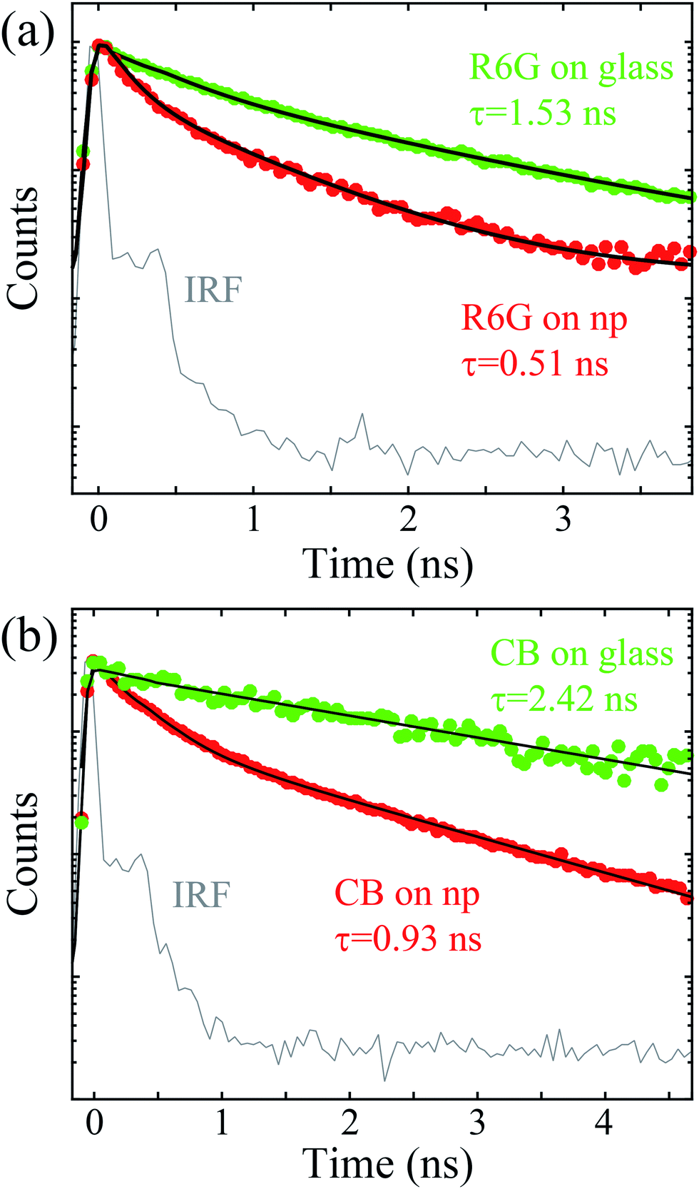 | ||
| Fig. 5 Amplitude-normalized fluorescence decays for (a) R6G and (b) CB deposited on glass and the nanoparticle grating. The green and red traces show the measured fluorescence decays for the deposited fluorophores on alumina coated glass and on nanoparticles, respectively. The black lines show the numerical fits obtained using eqn (5) for the measured data. IRF denotes the instrument response function. | ||
These lifetimes are presented in Table 1. The intrinsic lifetimes of both fluorophores were measured from 1 μM fluorophore solution in DIW. The measured lifetimes for R6G and CB were 3.98 ns and 3.86 ns, respectively, and the measured lifetime for R6G corresponds very well to previously reported values.33 When the fluorophores are deposited on a glass surface, the mean lifetimes of R6G and CB decrease to 1.53 ns and 2.42 ns, respectively. These lifetime decreases most likely originate from the reduced photonic mode density (PMD) upon the fluorophore immobilization on the glass surface37 and quenching effect from oxygen. As CB is designed to resist quenching upon immobilization, the relative drop in lifetime when it is placed on a glass surface is less in comparison with R6G. Upon the deposition of R6G onto the Λ = 370 nm grating, the lifetime decreases from 1.53 ns to 0.51 ns. Similarly, the CB lifetime decreases from 2.42 ns to 0.93 ns following deposition onto the Λ = 1 μm grating. For both fluorophores this corresponds approximately to a 3-fold decrease in lifetime. These results are in qualitative accordance with the increased fluorescence intensities attained using the steady-state measurements indicating a coupling between the fluorophores and silver nanoparticles.
![[small tau, Greek, macron]](https://www.rsc.org/images/entities/i_char_e0d4.gif) (ns) and goodness of the fit χR2
(ns) and goodness of the fit χR2
| Sample | τ1 (x1) | τ2 (x2) | |
χR2 |
|---|---|---|---|---|
| Rhodamine 6G | ||||
| In 1 μM DIW solution | 3.98 (100%) | — | 3.98 | 0.97 |
| On glass | 1.72 (63%) | 0.62 (37%) | 1.53 | 1.16 |
| On nanoparticles | 0.79 (20%) | 0.15 (80%) | 0.51 | 1.22 |
|
||||
| Cascade Blue | ||||
| In 1 μM DIW solution | 3.86 (100%) | — | 3.86 | 1.06 |
| On glass | 2.44 (94%) | 0.41 (6%) | 2.42 | 1.11 |
| On nanoparticles | 1.35 (23%) | 0.25 (77%) | 0.93 | 1.91 |
While the fluorescence decay of the dyes in aqueous media exhibits only a single exponential decay, a biexponential model is required to satisfactorily fit the fluorescence decays on glass and nanoparticle gratings. Both the glass and nanoparticle samples exhibit a decay that is composed of fast and slow components indicating two different quenching mechanisms (e.g. the changed PMD on glass and oxygen quenching). Especially, the decreased magnitude of the longer lifetime component on glass is proportional to the reduced relative local density of states of the molecules on an alumina coated glass surface (factor of ∼1.4–1.5).38 Interestingly, both lifetime components are shortened when the molecules are placed in the vicinity of the nanoparticles. For both fluorophores, the shorter lifetime component accounts for roughly 80% of the whole decay, which indicates a strong fluorophore–nanoparticle coupling and efficient fluorescence enhancement.
A wide range of experimentally measured enhancement values have been reported in the literature. For example, a 40-fold enhancement has been measured using a near-infrared fluorophore IR800 with Au nanoshells.11 Moreover, approximately 100-fold enhancements have been demonstrated using cyanine dyes coupled to periodic arrays of Ag NPs.20 Lower enhancement values have also been demonstrated that range from 3.5-fold39 to 10-fold40 to 14-fold.8 These order of magnitude differences can be partly explained by the fluorophore used in the experiments, i.e., the fluorophores with low quantum yield have demonstrated the highest enhancement values. In this respect, the measured enhancement factors for the Λ = 370 nm grating are comparable or even better than other results published for similar structures, especially when dealing with near-unity quantum yield fluorophores.
According to the literature, the lower quantum yield of CB molecules should enable higher enhancement factors than those observed in the measurements. The relatively low enhancement factor for CB molecules could originate from the multipolar resonant plasmonic mode exhibiting low scattering efficiency as suggested by previous research.41 This would further suggest that multipolar plasmonic resonances are not suitable for enhancing molecular fluorescence.
It is difficult to determine the exact contribution of each mechanism related to the fluorescence enhancement, such as absorption enhancement, additional radiative pathways or enhanced emission to the far field, since these processes are linked together. In the case of R6G, however, it is safe to argue that the contribution of the enhanced absorption at the excitation wavelength is responsible almost entirely for the observed enhancement of fluorescence.42
For both gratings the actual interparticle distances are too large to enable efficient coupling between the particles. Moreover, the dimensions of the particles and the 2D grating do not support any coupling between the LSPR and grating diffraction orders to give rise to surface lattice resonances as evidenced by the extinction spectra. Hence, the near field induced by the LSPR is mostly responsible for the local field enhancement experienced by the fluorophores. This makes these substrates non-optimal for SERS for example, but more suitable for MEF applications.
4 Conclusions
We have developed a method to produce periodic silver nanostructures on a large-scale (in the range of cm2) to be employed in various surface enhancing spectroscopy techniques. In this work, we have demonstrated their applicability for enhancing molecular fluorescence. The fabricated structures exhibit good long-range order and are highly symmetrical. Moreover, the size of the structures can be varied in a controlled fashion in order to tune their optical response. We have demonstrated that the periodicity Λ of the 2D gratings can be varied between 370 nm and 1 μm. Nevertheless, the lowest attainable grating spacing that is obtainable with this setup is roughly 250 nm. Naturally, this limit can be reduced by using a laser source with a shorter wavelength. The measured average fluorescence enhancement value for R6G molecules using a Λ = 370 nm grating is approximately 14, which is comparable to the values reported in the literature for similar structures and fluorophores. For a grating with Λ = 1 μm with CB molecules, the average fluorescence intensity is roughly doubled. Furthermore, the time-resolved fluorescence measurements displayed a shortening of the lifetime for both of the fluorophores when deposited on the nanoparticle grating.The proposed method is cost-effective and fast in comparison to EBL or optical lithography and does not require the use of UV-sources or additional masks. In addition, the fabrication technique does not require any post-processing steps as in conventional interference lithography or lift-off as in EBL. Hence replacing the photoresist with azopolymer significantly mitigates the fabrication process requirements. Furthermore, once the SRG has been inscribed on the azopolymer film, it will not deteriorate for months if stored properly. Finally, with a sufficiently powerful excitation source this technique can be scaled up to process whole wafers. In the future other materials, such as Al, Au, and Cu, could be tested for sensing or surface enhanced spectroscopic applications using this fabrication process.
Acknowledgements
Aleksandr Kravchenko is kindly acknowledged for the fruitful discussions related to the fabrication process. The authors gratefully acknowledge the financial support from the Aalto ELEC Doctoral School and Academy of Finland project numbers 285972 and 13251864. This work made use of the Aalto University Micronova Nanofabrication Center and Aalto University Nanomicroscopy Center (Aalto-NMC) premises.References
- E. M. C. Hillman and A. Moore, Nat. Photonics, 2007, 1, 526–530 CrossRef CAS PubMed.
- G. MacBeath and S. L. Schreiber, Science, 2000, 289, 1760–1763 CAS.
- R. P. Hertzberg and A. J. Pope, Curr. Opin. Chem. Biol., 2000, 4, 445–451 CrossRef CAS PubMed.
- V. Pale, T. Nikkonen, J. Vapaavuori, M. Kostiainen, J. Kavakka, J. Selin, I. Tittonen and J. Helaja, J. Mater. Chem. C, 2013, 1, 2166–2173 RSC.
- J. R. Lakowicz, Principles of Fluorescence Spectroscopy, Springer Science & Business Media, 3rd edn, 2006 Search PubMed.
- V. Pale, T. Nikkonen, J. Helaja and I. Tittonen, 2014 IEEE 14th International Conference on Nanotechnology (IEEE-NANO), 2014, pp. 225–228 Search PubMed.
- J. R. Lakowicz, Anal. Biochem., 2001, 298, 1–24 CrossRef CAS PubMed.
- K. Ray, H. Szmacinski and J. R. Lakowicz, Anal. Chem., 2009, 81, 6049–6054 CrossRef CAS PubMed.
- S. Nie and S. R. Emory, Science, 1997, 275, 1102–1106 CrossRef CAS PubMed.
- F. Tam, G. P. Goodrich, B. R. Johnson and N. J. Halas, Nano Lett., 2007, 7, 496–501 CrossRef CAS PubMed.
- R. Bardhan, N. K. Grady, J. R. Cole, A. Joshi and N. J. Halas, ACS Nano, 2009, 3, 744–752 CrossRef CAS PubMed.
- Y. Chen, G. Kang, A. Shah, V. Pale, Y. Tian, Z. Sun, I. Tittonen, S. Honkanen and H. Lipsanen, Adv. Mater. Interfaces, 2014, 1, 1300008 Search PubMed.
- L. Novotny and B. Hecht, Principles of nano-optics, Cambridge university press, 2nd edn, 2012 Search PubMed.
- P. Anger, P. Bharadwaj and L. Novotny, Phys. Rev. Lett., 2006, 96, 113002 CrossRef PubMed.
- J. R. Lakowicz, Anal. Biochem., 2005, 337, 171–194 CrossRef CAS PubMed.
- K.-S. Lee and M. A. El-Sayed, J. Phys. Chem. B, 2006, 110, 19220–19225 CrossRef CAS PubMed.
- S. A. Maier, Plasmonics: fundamentals and applications, Springer Science & Business Media, 2007 Search PubMed.
- T. Xu, Y.-K. Wu, X. Luo and L. J. Guo, Nat. Commun., 2010, 1, 59 Search PubMed.
- Y. Xia, J. A. Rogers, K. E. Paul and G. M. Whitesides, Chem. Rev., 1999, 99, 1823–1848 CrossRef CAS PubMed.
- T. Corrigan, S. Guo, R. Phaneuf and H. Szmacinski, J. Fluoresc., 2005, 15, 777–784 CrossRef CAS PubMed.
- W. Q. Li, G. Wang, X. N. Zhang, H. P. Geng, J. L. Shen, L. S. Wang, J. Zhao, L. F. Xu, L. J. Zhang, Y. Q. Wu, R. Z. Tai and G. Chen, Nanoscale, 2015, 7, 15487–15494 RSC.
- H. Schift, J. Vac. Sci. Technol., B: Microelectron. Nanometer Struct.--Process., Meas., Phenom., 2008, 26, 458–480 CrossRef CAS.
- J. Cheng, C. Ross, H. Smith and E. Thomas, Adv. Mater., 2006, 18, 2505–2521 CrossRef CAS.
- Z. Mahimwalla, K. G. Yager, J.-i. Mamiya, A. Shishido, A. Priimagi and C. J. Barrett, Polym. Bull., 2012, 69, 967–1006 CrossRef CAS.
- G. S. Hartley, Nature, 1937, 140, 281 CrossRef CAS.
- H. v. Wolferen and L. Abelmann, Lithography: Principles, processes and materials, Nova Science Publishers, 2011 Search PubMed.
- A. Kravchenko, A. Shevchenko, V. Ovchinnikov, A. Priimagi and M. Kaivola, Adv. Mater., 2011, 23, 4174–4177 CrossRef CAS PubMed.
- A. Kravchenko, A. Shevchenko, P. Grahn, V. Ovchinnikov and M. Kaivola, Thin Solid Films, 2013, 540, 162–167 CrossRef CAS.
- R. J. Moerland, J. E. Koskela, A. Kravchenko, M. Simberg, S. van der Vegte, M. Kaivola, A. Priimagi and R. H. A. Ras, Mater. Horiz., 2014, 1, 74–80 RSC.
- C. Kauppinen, T. Haggren, A. Kravchenko, H. Jiang, T. Huhtio, E. Kauppinen, V. Dhaka, S. Suihkonen, M. Kaivola, H. Lipsanen and M. Sopanen, Nanotechnology, 2016, 27, 135601 CrossRef PubMed.
- A. Priimagi and A. Shevchenko, J. Polym. Sci., Part B: Polym. Phys., 2014, 52, 163–182 CrossRef CAS.
- R. Kubin and A. Fletcher, J. Lumin., 1983, 27, 455–462 CrossRef CAS.
- D. Magde, R. Wong and P. G. Seybold, Photochem. Photobiol., 2002, 75, 327–334 CrossRef CAS PubMed.
- J. E. Whitaker, R. P. Haugland, P. L. Moore, P. C. Hewitt, M. Reese and R. P. Haugland, Anal. Biochem., 1991, 198, 119–130 CrossRef CAS PubMed.
- L. Zhao, K. L. Kelly and G. C. Schatz, J. Phys. Chem. B, 2003, 107, 7343–7350 CrossRef CAS.
- B. Auguié and W. L. Barnes, Opt. Lett., 2009, 34, 401–403 CrossRef.
- W. L. Barnes, J. Mod. Opt., 1998, 45, 661–699 CrossRef CAS.
- R. J. Moerland and J. P. Hoogenboom, Optica, 2016, 3, 112–117 Search PubMed.
- Y. Teng, K. Ueno, X. Shi, D. Aoyo, J. Qiu and H. Misawa, Ann. Phys., 2012, 524, 733–740 CrossRef CAS.
- P. Bharadwaj, P. Anger and L. Novotny, Nanotechnology, 2007, 18, 044017 CrossRef.
- G. Sun, J. B. Khurgin and C. C. Yang, Appl. Phys. Lett., 2009, 95, 171103 CrossRef.
- D. Darvill, A. Centeno and F. Xie, Phys. Chem. Chem. Phys., 2013, 15, 15709–15726 RSC.
Footnote |
| † Electronic supplementary information (ESI) available: Statistical analysis of the SEM images, AFM data and statistical analysis data of the confocal microscopy data. See DOI: 10.1039/c6ra04202c |
| This journal is © The Royal Society of Chemistry 2016 |