CdIn2S4 quantum dots: novel solvent-free synthesis, characterization and enhancement of dye-sensitized solar cells performance

Mehdi Mousavi-Kamazania, Zabihullah Zarghamib, Masoud Salavati-Niasari*c and Omid Amiric
aYoung Researchers and Elites Club, Kashan Branch, Islamic Azad University, Kashan, Iran
bYoung Researchers and Elites Club, Arak Branch, Islamic Azad University, Arak, Iran
cInstitute of Nano Science and Nano Technology, University of Kashan, Kashan, P. O. Box. 87317-51167, I. R. Iran. E-mail: salavati@kashanu.ac.ir; Fax: +98 31 55913201; Tel: +98 31 55912383

Received 12th February 2016 , Accepted 21st March 2016

First published on 1st April 2016


Abstract

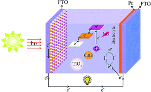
Herein, CdIn2S4 (CdIS) quantum dots were synthesized via a solid-state thermal decomposition approach for the first time. [Cd(en)2]SO4, In(NO3)3·5H2O and thioacetamide were used as the cadmium, indium and sulfur sources. The as-synthesized products were characterized extensively by techniques such as XRD, EDS, SEM, TEM, AFM, FTIR and DRS. The effect of the cadmium source type, temperature and reaction atmosphere on the morphology and purity of the final products were studied. The results showed that choosing the appropriate temperature and cadmium source has a significant influence on CdIS–QDs synthesis. Moreover, the as-prepared CdIS–QDs were utilized as a barrier layer in dye sensitized solar cells (DSSCs) for the first time. The short-circuit photocurrent density (Jsc), open-circuit voltage (Voc), fill factor (FF) and efficiency of the solar cell were studied. The power conversion efficiency of the DSSCs using a CdIS–QDs barrier layer was 8.17%, which is 32.2% higher than the cell without a novel barrier layer (6.18%).


Introduction

Conventional dye-sensitized solar cells (DSSCs) have attracted extensive scientific attention and technical interest over the past two decades as one of the most encouraging third generation solar cells, due to the superior properties compared with silicon based solar cells such as low cost, relatively high efficiency, flexibility and easy fabrication.1–3 In general, a DSSC consists of an n-type semiconductor with a large band-gap (also named photoanode), dye molecules as a sensitizer, a redox electrolyte and a counter electrode.4,5 Titanium dioxide (TiO2), a wide band-gap (3.0–3.2 eV) n-type semiconductor, is one of the most prominent oxide materials for performing various types of industrial applications such as photovoltaics,6 photocatalysis7,8 and photochromic applications.9 When TiO2 photoanodes are used in DSSCs, the electron transfer between the excited dyes to the conduction band of TiO2 is ultra-fast (femto seconds), but the recombination of the injected electron with the electrolyte is high because of the low electron mobility of TiO2. To decrease the recombination rate of the electron, some metal oxide materials, such as Al2O3,10 ZrO2, SiO2, and ZnO,11 have been coated on the TiO2 film as a barrier layer. However, barrier layer materials, such as Al2O3 and ZnO, not only decrease the electronic coupling between the dye and TiO2, but also suppress the electron transport from the excited dyes to conduction band of TiO2 because of the lower electron transport rate and modifying the TiO2 electronic structure.12,13 Recently, materials, such as CuInS2,13,14 AgInS2 (ref. 15) and CuIn2S4,16 with long-term stability and high light-absorbing properties are utilized excellently in thin film solar cells. Moreover, the conduction band levels of these materials is higher than that of TiO2, indicating that the electron can be injected from them into the TiO2 conduction band rapidly and efficiently. Therefore, their quantum dots (QDs) can act as an energy barrier layer like the position of the ZnO barrier layer to block the recombination of photo injected electrons with redox ions in the electrolyte and hole formed in excited dyes. Cadmium indium sulfide (CdIn2S4) is the a semiconducting chalcogenide compound and owing to its excellent properties in solar cells and optoelectronic applications,13,16 considerable attempts have been made to synthesize CdIn2S4 QDs with various morphologies, including spherical,16 rod-like,17 flower-like18 and sheet-like.19 To date, the CdIn2S4 nanostructure has been synthesized by methods such as hydrothermal,20 solvothermal21 microwave22 and sol gel templating.23 In most cases, these techniques require expensive solvents and precursors. To the best of our knowledge, the solid-state thermal decomposition approach for synthesizing CdIn2S4 (CdIS) QDs and other ternary compounds has not been reported yet and in this present study, we conducted the CdIS–QDs preparation using a simple, low-cost and solvent-less route by thermal decomposing a mixture of thioacetamide (TAA), [Cd(en)2]SO4 and In(NO3)3·5H2O under argon atmosphere at 500 °C. Moreover, utilizing CdIS–QDs as a barrier layer has not been studied and for the first time we investigated the use of the as-prepared CdIS–QDs as a barrier layer in DSSCs. This method can be extended to the preparation of other ternary chalcogenide compounds.

Experimental

Materials and physical measurements

All the chemicals used in this method were of analytical grade and used the as-received without any further purification. The X-ray diffraction (XRD) patterns were recorded on a Philips-X'PertPro, X-ray diffractometer using Ni-filtered Cu Kα radiation at a scan range of 10° < 2θ < 80°. Energy dispersive spectrometry (EDS) analysis was studied using an X-Max Oxford, Philips microscope. Scanning electron microscopy (SEM) images were obtained on a LEO-1455VP equipped with an energy dispersive X-ray spectroscopy apparatus. Transmission electron microscope (TEM) images were obtained on a Philips EM208S transmission electron microscope with an accelerating voltage of 100 kV. Atomic force spectroscopy was performed by ARA-AFM, an Iranian made AFM (manufactured by Ara-Research Company in Tehran, Iran). The Fourier transform infrared (FT-IR) spectra were obtained on Magna-IR, spectrometer 550 Nicolet with 0.125 cm−1 resolution in KBr pellets in the range of 400–4000 cm−1. The diffused reflectance UV-visible spectrum (DRS) of the sample was recorded by an Ava Spec-2048TEC spectrometer. A photocurrent density–voltage (JV) curve was measured using computerized digital multimeters (Ivium-n-Stat Multichannel potentiostat) and a variable load. A 300 W metal xenon lamp (Luzchem) served as an assimilated sun light source and its light intensity (or radiant power) was adjusted to simulate AM 1.5 radiation at 100 mW cm−2 with a filter for this purpose.

Preparation of [Cd(en)2]SO4

0.01 mol of Cd(NO3)2·4H2O was dissolved in 20 mL of distilled water. 0.02 mol of ethylenediamine was dissolved in 20 mL of distilled water and was then added slowly to the obtained solution. The mixture was stirred and heated at 80 °C for 5 h. The obtained blue precipitate was centrifuged, washed several times with absolute ethanol and distilled water and dried at 50 °C.

Synthesis of CdIn2S4 QDs

The starting powders (0.08 g of [Cd(en)2]SO4, 0.2 g of In(NO3)·5H2O, and 0.08 g of TAA) were milled and mixed in a ball mill for 20 min using zirconia grinding media. Furthermore, the powder mixtures were calcined at 500 °C for 1.5 h under an argon atmosphere. Finally, it was washed several times with distilled water and absolute ethanol and dried at 70 °C for 10 h (sample 1). An experiment was performed with the same abovementioned procedure under atmospheric conditions (sample 2). To examine the temperature and cadmium source effect on the morphology and purity of the final products, two experiments were performed at 400 °C for 1.5 h under an argon atmosphere (sample 3) using Cd(NO3)2·4H2O instead [Cd(en)2]SO4 (sample 4).

Fabrication of FTTiO2

Electrophoresis deposition (EPD) was used to prepare the TiO2 films. During EPD, the cleaned FTO glass remained at a positive potential (anode), while a pure steel mesh was used as the counter (cathode) electrode. The linear distance between the two electrodes was about 3 cm. Power was supplied by a Megatek Programmable DC power supply (MP-3005D). The applied voltage was 10 V. The deposition cycle was repeated 4 times, each time for 15 s and the temperature of the electrolyte solution was maintained constant at 25 °C. The coated substrates were air dried. The apparent area of the film was 1 × 1 cm2. The resulting layer was annealed under an air flow at 500 °C for 30 min.

Fabrication of FTO/TiO2/N719/Pt

For the fabrication of FTO/TiO2/N719/Pt, the FTO/TiO2 prepared by EPD technique was immersed into a N-719 (Dyesol) dye solution in ethanol (0.5 mM) and maintained at 40 °C for 24 h. The counter electrode was made from the deposition of a Pt solution on FTO glass. Subsequently, this electrode was placed over the TiO2 electrode. Sealing was accomplished by pressing the two electrodes together on a double hot-plate at a temperature of about 110 °C. The redox electrolyte consisting of 0.05 M of LiI, 0.05 M of I2 and 0.5 M of 4-tert-butylpyridine in acetonitrile as a solvent was introduced to the cell through one of two small holes drilled in the counter electrode. Finally, these two holes were sealed by a small square of sealing sheet and characterized by an IV test.

Fabrication of FTO/TiO2/CdIn2S4 QDs/N719/Pt

The chemical bath method was employed to fabricate FTO/TiO2/CdIS–QDs/N719/Pt. For this purpose, the as-prepared QDs were sonicated at a power setting of 60 W in 40 mL of ethanol for 10 min. Subsequently, the prepared FTO/TiO2 via the EPD method was immersed in the obtained suspension for 5 h to deposit the QDs on the TiO2 surface. Finally, the obtained FTO/TiO2/CdIS–QDs was washed with a few drops of absolute ethanol and immersed in a N179 (Dyesol) dye solution in ethanol (0.5 mM) and maintained at 40 °C for 24 h.

Results and discussion

Synthesis and characterization of nanostructures

The crystal structure and phase composition of the obtained products were determined by XRD. Fig. 1a and b show typical XRD patterns of the obtained products in the presence (sample 1) and absence of argon gas (sample 2), respectively.
image file: c6ra03894h-f1.tif
Fig. 1 XRD patterns of the as-synthesized samples: (a) in presence of argon gas (sample 1) and (b) in absence of argon gas (sample 2) at 500 °C.

As shown in Fig. 1a, in the presence of argon gas, a pure cubic phase of CdIn2S4 with the space group, Fd3m, JCPDS no. 27-0060 and the cell parameter a = 10.8450 Å was obtained. Moreover, no crystalline impurity phases were observed in the product, indicating the relatively high purity of the CdIn2S4 nanostructures. When the experiment was performed in the absence of argon gas, pure cubic phase of In2O3 with the space group of Ia[3 with combining macron], JCPDS no. 71–2194 and unit cell parameter of a = 10.1170 Å was synthesized (Fig. 1b). The crystallite sizes of the as-synthesized CdIn2S4 nanoparticles were estimated to be 7 nm by the Scherer formula shown in eqn (1).15

 
D(hkl) = /β[thin space (1/6-em)]cos[thin space (1/6-em)]θ (1)
where D is the crystallite size, as calculated for the (hkl) reflection, k is the wavelength of Cu Kα radiation (0.154 nm), k is a constant related to the crystal shape (0.94), and β is the full width at half-maximum intensity (FWHM). The obtained XRD results show that for synthesizing pure CdIn2S4 QDs, the presence of argon gas is required.

Energy dispersive X-ray analysis (EDX) was used to determine the elemental composition and chemical purity of the obtained products. Fig. 2 shows a typical EDX spectrum of the as-synthesized product in the presence of argon gas (sample 1). As can be observed, only Cd, In and S peaks exist in the product, which shows that the CdIS–QDs were obtained without impurities. As expected, based on the calculation of the peak areas in Fig. 2, the ratio of Cd[thin space (1/6-em)]:[thin space (1/6-em)]In[thin space (1/6-em)]:[thin space (1/6-em)]S was found to be approximately 1[thin space (1/6-em)]:[thin space (1/6-em)]2[thin space (1/6-em)]:[thin space (1/6-em)]4. Therefore, both XRD and EDX analyses show that pure CdIn2S4 nanoparticles were synthesized successfully in the presence of argon gas via the mentioned synthetic route.


image file: c6ra03894h-f2.tif
Fig. 2 EDX spectrum of the as-synthesized sample annealed at 500 °C in the presence of argon gas (sample 1).

To study the surface nature of the as-prepared CdIS–QDs (sample 1) and the valence states of elements in CdIn2S4 nanostructures, the sample was characterized by X-ray photoelectron spectroscopy (XPS). The core levels of Cd 3d, In 3d, and S 2p were examined. As shown in the survey spectrum (Fig. 3a) with peak identification, the oxygen peak at a binding energy of 532.5 eV was attributed to the presence of H2O absorbed on the sample surface and no obvious impurities can be detected. The peak areas of these high-resolution scans were measured and used to calculate the elemental ratio of the nanocrystals. The quantification of the peaks obtains the ratio of Cd[thin space (1/6-em)]:[thin space (1/6-em)]In[thin space (1/6-em)]:[thin space (1/6-em)]S as 1[thin space (1/6-em)]:[thin space (1/6-em)]1.9[thin space (1/6-em)]:[thin space (1/6-em)]3.89, which closely agrees with that obtained from EDX analysis. From the elemental analyses (XPS) results, we can conclude that the composition of CdIn2S4 nanocrystals is close to the stoichiometric proportion of individual atoms. The Cd 3d core (Fig. 3b) splits into 3d5/2 (405.6 eV) and 3d3/2 (412.1 eV) peaks, which are all in good agreement with the reported values for Cd2+.


image file: c6ra03894h-f3.tif
Fig. 3 XPS spectrum of the sample annealed at 500 °C in the presence of argon gas (sample 1) (a) survey spectrum; (b) Cd 3d; (c) In 3d; and (d) S 2p.

Moreover, Fig. 3c shows that the peaks centered at 443.8 and 451.7 eV are in good accordance with In 3d5/2 and In 3d3/2. The single S 2p peak (Fig. 3d) at 161 eV is indicative of sulfur present as a sulfur ion.19

Fig. 4a–c show FTIR spectra of the samples before annealing, after annealing at 400 °C in Ar gas (sample 3) and after annealing at 500 °C in Ar gas (sample 1), respectively. As shown, before annealing (Fig. 4a), due to the presence of ethylenediamine in the precursors, all the absorption bands are related to ethylenediamine, including two absorption bands located in 3315 and 3364 cm−1 related to the N–H stretching of primary amine (–NH2) and the two bands at 2935 and 2844 cm−1 correspond to the –CH2 asymmetric and symmetric stretching modes.24


image file: c6ra03894h-f4.tif
Fig. 4 FTIR spectra of samples: (a) before annealing, (b) annealed at 400 °C (sample 3) and (c) annealed at 500 °C in argon gas (sample 1).

The absorption band at 1604 cm−1 was assigned to N–H bending band of –NH2 and the band at 1145 cm−1 is related to the C–N stretching mode.25 Fig. 4b (annealed at 400 °C in Ar gas, sample 3) shows that the ethylenediamine were not removed completely and there are trace amounts of organic materials in the final product. Finally, after annealing at 500 °C in Ar gas (sample 1), all the organic molecules were well removed and no significant absorption bands could be observed in the FTIR spectrum of the as-obtained product (Fig. 4c).

Fig. 5a shows a SEM image of the as-synthesized CdIS–QDs (sample 1). As shown, uniform nanoparticles with particles sizes in the range of 7–10 nm were obtained. To examine the particle size and morphology in more detail, the CdIS–QDs (sample 1) were characterized by TEM (Fig. 5b). As presented, the highly monodisperse nanoparticles with an approximate size of 8 nm were synthesized, concurring with the SEM image. Fig. 5c shows high resolution TEM (HRTEM) image of the as-prepared CdIS–QDs (sample 1) and the lattice fringes of the CdIn2S4 nanostructures reveal the highly crystalline nature of the particles. The spacing between the two adjacent lattice planes was 0.324 nm, which corresponds to the (311) plane of cubic CdIn2S4. To determine the particle size distribution, we performed DLS analysis, which is based on the scattering of the laser light in an aqueous solution. Fig. 6 exhibits the DLS results of CdIS–QDs (sample 1). The mean particle size for nanoparticles was 10 nm. In this technique, the particles are illuminated with a laser. Furthermore, the hydrodynamic diameter of the particles was calculated using the intensity fluctuations of scattered light arising from Brownian motion and the Stokes–Einstein equation.


image file: c6ra03894h-f5.tif
Fig. 5 (a) SEM image, (b) TEM and (c) HR-TEM images of the as-synthesized sample annealed at 500 °C in argon gas (sample 1).

image file: c6ra03894h-f6.tif
Fig. 6 Size distribution of CdIS–QDs (sample 1).

The diameter obtained by this technique is sphere-like and has the same translational diffusion coefficient as the particle being measured. The translational diffusion coefficient depends not only on the size of the particle (core), but also on the surface structure, as well as the concentration and type of ions in the liquid medium. This means that the size of the sample could be larger than when it is measured by electron microscopy or any other microscopic technique.

The XRD pattern of the sample obtained at 400 °C (sample 3) is presented in Fig. 7a. As it can be observed, conducting the experiment at 400 °C results in impurity formation and CdS as an undesired product is formed. Fig. 7b shows a SEM image of sample prepared after annealing at 400 °C (sample 3). As can be observed, the nanoparticles were obtained but in some parts, aggregation was observed and the nanoparticles were not uniform. This can be related to presence of a trace amount of ethylenediamine on the nanoparticles surface, which can promote aggregation. These results show that the SEM image and FTIR spectra are in good agreement with each other.


image file: c6ra03894h-f7.tif
Fig. 7 (a) XRD pattern and (b) SEM image of the as-synthesized sample annealed at 400 °C in argon gas (sample 3).

As a result, the annealing temperature has a remarkable influence on the final product morphology and purity and 500 °C is a preferable temperature to prepare CdIS–QDs via mentioned synthetic method. To evaluate the precursor effect, an experiment was carried out using Cd(NO3)2·4H2O (sample 4) as a direct cadmium precursor without further modification, instead of [Cd(en)2]SO4. The XRD pattern of obtained product using Cd(NO3)2·4H2O (sample 4) is shown in Fig. 8a. As can be observed, the use of Cd(NO3)2·4H2O led to the formation of impurities and In2O3 and CdS along with CdIn2S4 were produced. Moreover, the morphology of the sample prepared using Cd(NO3)2·4H2O was characterized by SEM and the obtained image is presented in Fig. 8b. As can be observed, the nanoparticles and microparticles were obtained and the nanoparticles are aggregated together. These findings show that precursor type play crucial role on CdIS–QDs synthesis and choosing an appropriate precursor is essential to obtain a preferable product.


image file: c6ra03894h-f8.tif
Fig. 8 (a) XRD pattern and (b) SEM image of as synthesized sample using Cd(NO3)2·4H2O as cadmium source (sample 4).

Solar cell section

EDX analysis was used to identify the elemental composition of the FTO/TiO2/CdIn2S4 structure, as shown in Fig. 9.
image file: c6ra03894h-f9.tif
Fig. 9 EDX spectrum of the as-prepared FTO/TiO2/CdIn2S4 electrode.

The presence of Ti, O and Sn shows that TiO2 was successfully deposited on the glass substrate. Moreover, presence of Cd, In and S indicates that CdIn2S4 was successfully deposited on the TiO2 film.

The morphology and cross-section of the fabricated film (FTO/TiO2) were investigated by SEM. As shown in Fig. 10a, the TiO2 film consist spherical nanoparticles that were deposited uniformly on the glass substrate. Fig. 10b shows a SEM image of a cross-section of the TiO2 nanoparticles electrode, which shows that the thickness of the fabricated P25 electrodes with 4 cycles for 15 s electrophoresis was 9.3 μm. For more investigation of the surface morphology and topography, the bare TiO2 and TiO2/CdIS–QDs electrodes were characterized by AFM and the 2D and 3D AFM images are presented in Fig. 11a and b. As can be observed, the bare TiO2 electrode shows a uniform surface with hierarchical structure (Fig. 11a). In addition, its porosity is high, which can improve the CdIn2S4 absorption on the surface and increase the solar cell efficiency. Fig. 11b shows an AFM image of the TiO2/CdIn2S4 electrode. As shown in Fig. 11b, the smoothness of the surface was improved. In other words, the ups and downs of the TiO2 surface was well filled with CdIn2S4 and the CdIS–QDs were successfully loaded in the pores of TiO2.


image file: c6ra03894h-f10.tif
Fig. 10 (a) SEM image of TiO2 film and (b) SEM micrograph of cross-section of the TiO2 nanoparticles electrode.

image file: c6ra03894h-f11.tif
Fig. 11 AFM images of (a) bare TiO2 electrode, and (b) TiO2/CdIn2S4 electrode.

The UV-vis absorption spectra of CdIS–TiO2 and bare TiO2 are shown in Fig. 12, which exhibit absorption edges at around 460 nm for CdIS–TiO2 and no significant absorption for the bare TiO2.


image file: c6ra03894h-f12.tif
Fig. 12 UV-vis absorption spectrum of the FTO/TiO2 and FTO/TiO2/CdIn2S4 electrodes.

These results show that by depositing the CdIS–QDs on the TiO2 surface, light harvesting in the visible light region is enhanced and the solar cell efficiency is improved. For performance comparison between the DSSCs fabricated with and without using CdIS–QDs, current density–voltage (JV) curves were obtained and are presented in Fig. 13.


image file: c6ra03894h-f13.tif
Fig. 13 JV characterization of FTO/TiO2/N719 and FTO/TiO2/CdIS/N719.

As the results show, by depositing CdIS–QDs between TiO2 and N719, all Jsc, Voc and FF parameters and consequently the final efficiency (eqn (2)) showed remarkable enhancement from, 18.72 mA, 0.57 V, 0.58 and 6.18% to 20.96 mA, 0.65 V, 0.6 and 8.17%, respectively. CdIS–QDs as a barrier layer form intermediate levels (Fig. 14), and as a result, the excitation lifetime of the electron will be increased significantly and so the improvement of Jsc is expected.13 In addition, by depositing quantum dots between the TiO2 and dyes, the Fermi levels increase, leading to an increase in Voc. Moreover, as noted earlier, quantum dots fill well the TiO2 surface hills and valleys and consequently improve the FF value.26 Finally, enhancement in the Jsc, Voc and FF parameters results in an improvement in efficiency from 6.18% to 8.17%.

 
η = Jsc × Voc × FF/I0 × 100 (2)


image file: c6ra03894h-f14.tif
Fig. 14 Successive adsorption of CdIn2S4 QDs along with dye on the FTO/TiO2.

UV-vis spectroscopy was used to evaluate the dye molecules absorbed on the working electrodes. An alkaline solution was prepared by dissolving 0.05 g NaOH in 100 mL distilled water and the electrodes were then immersed in 10 mL of the solution for 24 h separately.27 Subsequently, the desorbed dye solution was characterized by UV-vis spectroscopy (Fig. 15). The results are presented in Fig. 15. Higher absorbance coefficient in the spectra shows the higher dye adsorption on the film. As can be observed from the Fig. 15, the cell reference absorbs a higher amount of dye, while cell, including CdIS–QDs, show a better PCE. Based on these results, we can conclude that the performance enhancement in DSSCs is due to the light harvesting property of CdIS–QDs.


image file: c6ra03894h-f15.tif
Fig. 15 UV-vis of the dye solution desorbed from different cells.

Electrochemical impedance spectroscopy (EIS) was used to elucidate the interfacial charge transfer processes in the devices.27 Fig. 16 demonstrates typical Nyquist plots of the DSSCs with bare TiO2 and cells containing CdIS–QDs. With increasing frequency, two semicircles are observed in the Nyquist plots. The first semicircle was assigned to the charge transfer resistance between the platinum counter electrode and redox couple (RCE). In the middle frequency region, the second semicircle reflecting the charge transfer resistance at the dyed-TiO2/electrolyte interface is related to the charge recombination process (RCT). The impedance spectra of these devices with the best energy conversion efficiency were investigated. The impedance spectra were fitted to a simplified version of the equivalent circuit. Some important parameters of the working electrodes in these devices were determined from the second semicircles and are summarized in Fig. 16 and Table 1. The effective diffusion coefficient of electrons (Deff) can be determined using eqn (2):

Deff = [RCT/RCE]L2keff
where, keff is the reaction rate constant for electron recombination with triiodide and L is the film thickness.27


image file: c6ra03894h-f16.tif
Fig. 16 Typical Nyquist plots of the DSSCs with bare TiO2 and cells containing QDs.
Table 1 Electrochemical parameters obtained by fitting the impedance spectra of DSSCs
DSCs τ (s) keff (S−1) RCE (Ω cm2) RCT (Ω cm2) Deff (cm2 s−1)
Reff 0.042 23.80 13 72 12.7 × 10⁻⁵
QDs/GNPs/GNRs 0.075 13.33 55 156 3.78 × 10⁻⁵


There is small difference between these devices for the RCE at the counter electrode/electrolyte interface. These results show that the CdIS–QDs do not make the over potential at the counter electrode. It can be noted that the fitted value of RCT for the cell containing the CdIS–QDs was ∼156 Ω cm2, while the corresponding value for reference cell was ∼72 Ω cm2. This significant increase in RCT shows that the CdIS–QDs are more favorable to suppressing the charge recombination process that arises from electrons in the TiO2 film with I in electrolyte solution, which leads to an increase in Jsc. On the other hand, the adsorption of CdIS–QDs on the TiO2 surface causes an increase in electron density in the conduction band of TiO2.

In the CdIS QDs-based cell, the middle-frequency peak in the Nyquist plot shifts to a lower frequency compared to reference device, exhibiting a longer electron lifetime for these cells.

Conclusion

In this study, CdIn2S4(CdIS) quantum dots were prepared via a solid-state thermal decomposition route for the first time. [Cd(en)2]SO4, In(NO3)3·5H2O and thioacetamide were used as precursors. The crystal structure, morphology, composition and optical properties of the as-synthesized products were characterized extensively by XRD, EDS, SEM, TEM, AFM, FTIR and DRS. The effect of precursor type, temperature and reaction atmosphere on the morphology and purity of final products were studied. Furthermore, for the first time, CdIS–QDs were employed as a barrier layer in DSSCs and their performance in solar cells was evaluated. The results showed that the CdIS–QDs with unique properties, such as high excitation lifetime, well pores filling and having intermediate levels, can enhance the FF, Jsc and Voc parameters and as a result, improve the final cell efficiency significantly from 6.18% to 8.17%.

Acknowledgements

The authors are grateful to the council of Iran National Science Foundation (91053846) and University of Kashan for supporting this study by Grant No. (159271/179).

Notes and references

  1. B. E. Hardin, H. J. Snaith and M. D. McGehee, Nat. Photonics, 2012, 6, 162 CrossRef CAS.
  2. S. F. Zhang, X. D. Yang, Y. Numata and L. Y. Han, Energy Environ. Sci., 2013, 6, 1443 CAS.
  3. B. O'Regan and M. Gratzel, Nature, 1991, 353, 737 CrossRef.
  4. R. Yu, Q. F. Lin, S. F. Leung and Z. Y. Fan, Nano Energy, 2012, 1, 57 CrossRef CAS.
  5. Q. F. Zhang, C. S. Dandeneau, X. Y. Zhou and G. Z. Cao, Adv. Mater., 2009, 21, 4087 CrossRef CAS.
  6. M. Gratzel, Nature, 2001, 414, 338 CrossRef CAS PubMed.
  7. N. Zhang, M. Q. Yang, S. Liu, Y. Sun and Y. J. Xu, Chem. Rev., 2015, 115, 10307 CrossRef CAS PubMed.
  8. J. A. Rengifo-Herrera and C. Pulgarin, Sol. Energy, 2010, 84, 37 CrossRef CAS.
  9. N. N. Wei, T. Han, G. Z. Deng, J. L. Li and J. Y. Du, Thin Solid Films, 2011, 519, 2409 CrossRef CAS.
  10. E. Palomares, J. N. Clifford, S. A. Haque, T. Lutz and J. R. Durrant, J. Am. Chem. Soc., 2003, 125, 475 CrossRef CAS PubMed.
  11. Y. Diamant, S. Chappel, S. G. Chen, O. Melamed and A. Zaban, Coord. Chem. Rev., 2004, 248, 1271 CrossRef CAS.
  12. J. A. Anta, E. Guillen and R. Tena-Zaera, J. Phys. Chem. C, 2012, 116, 11413 CAS.
  13. F. Guo, J. He, J. Li, W. Wu, Y. Hang and J. Hua, J. Colloid Interface Sci., 2013, 408, 59 CrossRef CAS PubMed.
  14. M. Mousavi-Kamazani, M. Salavati-Niasari, S. M. Hosseinpour-Mashkani and M. Goudarzi, Mater. Lett., 2015, 145, 99 CrossRef CAS.
  15. M. Mousavi-Kamazani and M. Salavati-Niasari, Composites, Part B, 2014, 56, 490 CrossRef CAS.
  16. L. Fan and R. Guo, J. Phys. Chem. C, 2008, 112, 10700 CAS.
  17. J. Q. Hu, B. Deng, W. X. Zhang, K. B. Tang and Y. T. Qian, Inorg. Chem., 2001, 40, 3130 CrossRef CAS PubMed.
  18. B. B. Kale, J. O. Baeg, S. M. Lee, H. Chang, S. J. Moon and C. W. Lee, Adv. Funct. Mater., 2006, 16, 1349 CrossRef CAS.
  19. W. Zhang, H. Yang, W. Fu, M. Li, Y. Li and W. Yu, J. Alloys Compd., 2013, 561, 10 CrossRef CAS.
  20. W. L. Jiang, X. H. Yin, F. Xin, Y. D. Bi, Y. Liu and X. Li, Appl. Surf. Sci., 2014, 288, 138 CrossRef CAS.
  21. S. Peng, S. G. Mhaisalkar and S. Ramakrishna, Mater. Lett., 2012, 79, 216 CrossRef CAS.
  22. S. K. Apte, S. N. Garaje and R. D. Bolade, et al., J. Mater. Chem., 2010, 20, 6095 RSC.
  23. J. M. Thornton and D. Raftery, Int. J. Hydrogen Energy, 2013, 38, 7741 CrossRef CAS.
  24. F. Mohandes and M. Salavati-Niasari, Ultrason. Sonochem., 2013, 20, 354 CrossRef CAS PubMed.
  25. A. Kianfar, H. Farrokhpour, P. Dehghani and H. R. Khavasi, Spectrochim. Acta, Part A, 2015, 150, 220 CrossRef CAS PubMed.
  26. M. Sabet, M. Salavati-Niasari and O. Amiri, Electrochim. Acta, 2014, 117, 504 CrossRef CAS.
  27. O. Amiri, M. Salavati-Niasari and M. Farangi, Electrochim. Acta, 2015, 153, 90 CrossRef CAS.

This journal is © The Royal Society of Chemistry 2016
Click here to see how this site uses Cookies. View our privacy policy here.