
 Open Access Article
 This Open Access Article is licensed under a
 Creative Commons Attribution 3.0 Unported Licence
Rapid thermal annealing assisted stability and efficiency enhancement in a sputter deposited CuO photocathode†
Saeid
Masudy-Panah
,
Roozbeh Siavash
Moakhar
,
Chin Sheng
Chua
,
Ajay
Kushwaha
,
Ten It
Wong
and
Goutam Kumar
Dalapati
*
Institute of Materials Research and Engineering, A*STAR (Agency for Science Technology and Research), 2 Fusionopolis Way, #08-03, Innovis, Singapore 138634, Singapore. E-mail: dalapatig@imre.a-star.edu.sg
First published on 16th March 2016
Abstract
We designed a stable and efficient CuO based photocathode by tuning the crystallinity and surface morphology of films by rapid thermal treatment. The role of the annealing temperature on film crystallinity, optical absorption and grain size is studied. The impact of these parameters upon the photocatalytic water splitting performance of CuO films is investigated. We observed that a higher annealing temperature improves the film crystallinity and increases the grain size of CuO film, which significantly enhance the photocurrent generation capability. Rapid thermal annealing at 550 °C is found the best temperature to achieve the highest PEC performance. The thickness of the CuO photocathodes is also optimized and we observed that 550 nm thick films results in the highest photocurrent of 1.68 mA cm−2. Our optimized CuO photocathode has shown better stability against photo-corrosion and a 30% decrease in the initial value of photocurrent is measured after 15 min, while a 60% decrease in the photocurrent is noticed in case of the as-deposited film.
Introduction
The growing need of energy necessitates a major technological development to secure sufficient renewable energy resources and combat the excessive use of fossil fuels. Fossil fuels are the main contributor in global warming and environmental pollution, which can be reduced by renewal energy. Solar energy is one of the most promising resources of renewable energy with the potential to meet the ever-growing global energy demands.1 Solar energy conversion using photoelectrochemical (PEC) water splitting is exciting technology that has the capability of harvesting the energy of solar radiation and store as chemical energy in the form of hydrogen and oxygen molecules.2,3 Efficient harvesting of solar light, stability against photocorrosion, low cost and earth abundance are main parameters for the selection of a photoelectrode materials which determine the ultimate energy conversion efficiency of the PEC process.4,5 Toward this, we have developed high performing and stable CuO photocathode through sputter deposition technique followed by rapid thermal treatment.Copper oxide is most promising candidate for fabricating photocathode due to its abundance in earth crust, non-toxicity, simple growth process and high optical absorption in visible range.6,7 The two most common forms of copper oxide are known as cuprous oxide (Cu2O) and cupric oxide (CuO). Cu2O is a direct band-gap semiconductor with the band gap energy of 2.1–2.6 eV and is predicted to produce a maximum theoretical photocurrent of 14.7 mA cm−2 under AM 1.5G illumination.6,8 On the other hand, CuO, an indirect band gap material, has a lower band gap energy of 1.2–1.6 eV, which makes it more ideal for visible light harvesting and renewable energy applications. CuO is theoretically capable of generating a much higher photocurrent of 35 mA cm−2.9 Its conduction band edge is also appropriate to do hydrogen evolution.8,10 Despite these promising properties of CuO, there are scant reports available on using CuO as the active light-harvesting material for PEC water splitting application.8,11–18 Most reports on CuO are merely interested in using it as a co-catalyst material for hydrogen evolution or solar cell application.19–29
Various methods are available for the deposition of CuO thin film including electrochemical deposition, evaporation, sputtering, thermal oxidation and sputter deposition.30–35 Sputtering method has attracted special interest due to its simplicity and reproducibility of the film properties. The sputtering process also allows precise tuning of the film's microstructure and its thickness by adjusting of the sputtering conditions.36–41 The performance of the PEC water splitting can be limited by the light absorption capabilities of the photoelectrodes and recombination of the photogenerated electrons and holes. These parameters are strongly affected by the thickness, grain size and crystallinity of the deposited film. Thus, a systematic investigation is required to address these issues to design a stable and efficient photoelectrode to demonstrate its potential for real PEC water splitting application. In similar context, a series of CuO thin films with different thicknesses ranging from 200 to 700 nm is sputter-deposited on the FTO substrate. After that rapid thermal treatment is performed to tune the crystalline property and surface morphology of CuO film. Heat treatment significantly improve the crystallinity of the film and grain size become larger which is very beneficial to enhance the PEC water splitting performance. The separation and transportation of photo-generated charge carrier is become prominent in rapid thermal annealed films and also reduce the charge recombination leading to an increase in photocurrent value and stability of the photocathode. Our investigation suggest that careful selection of film growth parameters and post growth modification can make CuO an attractive candidate for efficient water splitting application, which is not considered in previous studies.
Experimental
CuO thin film was sputtered onto FTO coated glass substrates to fabricate photoelectrode for PEC water splitting. Prior to the deposition process, the FTO substrates were cleaned through ultrasonication in IPA for duration of 10 min. The substrate was then dried with nitrogen gas before sputtering. A stoichiometric CuO target was used in Denton Discovery 18 sputtering system at sputtering power of 150 W with the evacuation pressure and working pressure at around 3 × 10⁻⁴ and 3.3 mTorr, respectively. The CuO films were then annealed in nitrogen ambient through rapid thermal annealing technique at 300, 550 and 700 °C for 1 min with the heating and cooling rate of 15 °C s−1 and 10 °C s−1, respectively. The CuO films with different thicknesses (from 200 to 700 nm) were also deposited by varying the deposition duration and then rapid thermal annealing were performed.Structural quality and crystallinity of the sputter-deposited CuO films were studied by Bruker D-8 general area detector XRD system (GADDS) in θ–2θ scan using a CuKα (λ = 0.15418 nm) radiation, high-resolution transmission electron microscopy (HRTEM) analysis and Raman spectroscopy measurements (Witec Alpha 300R confocal Raman microscope equipped with a 532 nm Nd:YAG laser). Surface morphology of the films was investigated by atomic force microscopy (AFM) and scanning electron microscope (SEM). Chemical composition of the CuO thin films were examined by using VG ESCALAB 220i-XL XPS system.
The photoelectrochemical properties of as-sputtered and rapid thermal annealed CuO films were evaluated in 0.1 M Na2SO4 aqueous electrolyte solution with a pH of 5.84 at room temperature by linear sweep voltammetry (LSV) and chronoamperometry (CA). LSV curves were measured at the scan rate of 50 mV s−1. CA plots were obtained at the potential of 0.2 V vs. RHE. Electrochemical impedance spectroscopy (EIS) was performed at open circuit potential and 10 mV amplitude over the frequency range of 105 to 10−2 Hz. All electrochemical measurements were carried out by Autolab 302N potentiostat/galvanostat equipped with FRA32M using a 3-electrode configuration consisting of a Pt counter electrode, an Ag/AgCl reference electrode and sputter-deposited CuO on FTO coated glass as the working electrode. An active area of 1 cm2 was defined by partially covering the film with black tape. Electrode edges have been fully covered by epoxy resin. The electrodes were then immersed in a 0.1 M Na2SO4 aqueous electrolyte solution with a pH of 5.84. The desired potential of the electrodes was supplied by A Metrohm Autolab PGSTAT101 potentiostat. NOVA 1.10 software was interfaced with the potentiostat to record the data and to be used for EIS fitting. Oriel solar simulator equipped with an air mass 1.5 global (AM 1.5G) filter and a 150 W xenon arc lamp were used to measure the current under light and dark condition. The light intensity was calibrated with a Si photo-diode and maintained at 100 mW cm−2.
Results and discussion
XRD pattern of as-deposited (AsD) and rapid thermal annealed CuO films deposited on FTO glass substrate are presented in Fig. 1. To clearly show the influence of annealing temperature on the crystallinity of the CuO film, we eliminated the XRD spectrum of FTO-coated substrate. All CuO films have two distinct peaks at 2-theta value of 35.482 and 38.764 degree which corresponds to the (002) and (111) plane for CuO, respectively (JCPDS# 05-0661). The corresponding full width half maximum (FWHM) of the XRD peaks are calculated as shown in Fig. 1b; the XRD peaks become intense and value of FWHM decreases at higher annealing temperature. This indicates that the crystallinity of the CuO film improves with increase in annealing temperature. However, intensity of both the XRD peaks are not constantly increased in all the films, as (111) peak become more intense in 550 °C while (002) peak is more prominent in 700 °C. Thus, we can say that different annealing temperature renders different orientation of the films. The transition of dominant orientation from (111) to (002) after annealing at higher temperature might be attributed to the difference between the surface binding energy of low index crystal planes. Higher mobility of adatoms is needed for the formation of oriented grains with higher binding energy. High annealing temperature enhances the energy transportation to adatoms which results in enhancement of the mobility of adatoms. The mobility of adatoms enhances at higher temperature which helps adatoms to reach the favorite lattice position more easily and induces (002) orientation.42 While at low annealing temperature, (111) orientation is preferred. The corresponding crystal size of the main XRD peaks of CuO (002) and CuO (111) of AsD and annealed films are determined from the Scherrer formula, D = Kλ/β![[thin space (1/6-em)]](https://www.rsc.org/images/entities/char_2009.gif) cosθ, where D, K, λ, β and θ are grain size, dimensionless shape factor, X-ray wavelength, line broadening at FWHM in radians and Bragg angle, respectively. Fig. 1c shows the effects of annealing temperature on the crystal size of the different CuO films which shows that higher annealing temperature renders larger size crystals/grains.
cosθ, where D, K, λ, β and θ are grain size, dimensionless shape factor, X-ray wavelength, line broadening at FWHM in radians and Bragg angle, respectively. Fig. 1c shows the effects of annealing temperature on the crystal size of the different CuO films which shows that higher annealing temperature renders larger size crystals/grains.
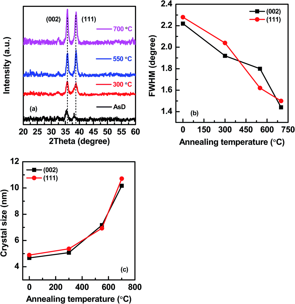 | ||
| Fig. 1 (a) XRD spectra of sputtered CuO films annealed at different temperature (300, 550 and 700 °C), (b) corresponding FWHM and (c) crystal size of the main XRD peaks of CuO (002) and CuO (111). | ||
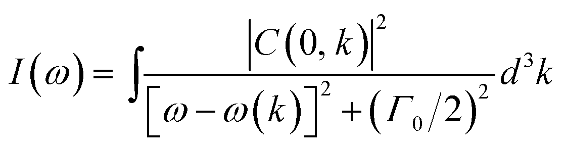
Raman analysis is an effective method of evaluating the effects of annealing temperature on the structural disorder, defects in the host lattice and crystallinity of the film. The Raman spectra of AsD CuO film and films annealed at various temperatures such as 300, 550 and 700 °C are shown in Fig. 2a. The distinct peaks, observed at ∼287, 339 and 623 cm−1 are associated with CuO thin film.43,44 CuO tenorite has monoclinic symmetry with space group of C62h with two molecules per primitive cell. Zone center modes of CuO is Ag + 2Bg + 4Au + 5Bu. Only Ag + 2Bg modes are Raman active.45 The Raman peak at 287 cm−1 is assigned to the Ag modes and the Raman peaks at 339 and 623 cm−1 are assigned to the Bg mode. For the CuO nanocrystals the Raman intensity I(ω) is given by:46
 | (1) |
| |C(k)|2 = exp(−k2d2/16π2) | (2) |
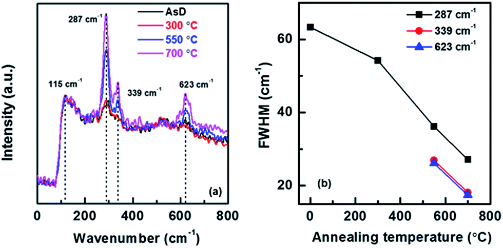 | ||
| Fig. 2 (a) Raman spectra CuO films annealed at different temperature (300, 550 and 700 °C) (b) FWHM plot calculated from Raman data of CuO films. | ||
The impact of the annealing temperature on the crystal quality of the CuO film is further observed from HR-TEM analysis. The HR-TEM image reveals clear and visible lattice fringes for CuO samples annealed at higher temperature (Fig. 3), indicating that the samples annealed at higher temperature have better atomic order and crystal quality. The crystal quality of the as-deposited film is affected by the mobility of ad-atoms along the grains. By increasing the annealing temperature, the ad-atoms become more mobile and migrates towards favorable sites in the crystal lattice, thus, resulting in an improvement in the crystallinity of the annealed samples at higher temperature.47 This improvement in crystal quality can result in the reduction of defect density and enhancement of carrier concentration of the CuO films annealed at higher temperatures.48 Based on the HR-TEM images shown in Fig. 3, the samples annealed at higher temperature of 500 and 700 °C are polycrystalline in nature with measured interplanar distances of ∼0.25 nm and 0.23 nm. This corresponds to the (002) and (111) planes of CuO, respectively.49,50
 | ||
| Fig. 3 High resolution transmission electron microscopic images show lattice spacing of CuO films, (a) AsD film and (b–d) films annealed at 300, 550 and 700 °C. | ||
Distinct surface morphology is observed in scanning electron microscopic (SEM) images of AsD and rapid thermal annealed CuO films (Fig. 4). The AsD CuO films has very smooth surface formed with nano-sized crystallites which are not visible clearly. Annealing at 300 °C, induce some roughness on the film surface and beginning of the large crystallites are appeared in the SEM images, the dark part in the images seems as initial grain boundaries. Further increase in annealing temperature, increase the surface roughness and grain boundaries becomes clearly visible. The grain size is surprisingly increase and grain boundaries become very prominent when film is annealed at 700 °C (Fig. 4d). Thus, SEM analysis validates our XRD and Raman results and endorses that gain size increased and crystalline property improved after heat treatment. The effect of annealing temperature on surface morphology of the 200 nm CuO thin film is also characterized by tapping mode AFM, respective change in grain size and surface roughness is noticeably visible (Fig. 5). The surface roughness is measured to be 5 nm, 21 nm, 40 nm, and 55 nm for AsD, and annealed at 300, 550 and 700 °C films, respectively. It shows that higher annealing temperature renders more rough film. The high annealing temperature provides more energy, which facilitates the coalescence of the adjacent grains (or nuclei), resulting in the larger grain size and rougher surface.
 | ||
| Fig. 4 Surface morphology of sputtered CuO films observed in top view scanning electron microscopic (SEM) images; (a) AsD films and (b–d) after rapid thermal treated at 300, 550 and 700 °C, respectively. | ||
 | ||
| Fig. 5 Surface topography and roughness measurement using tapping mode AFM; (a) AsD CuO film and (b–d) CuO films rapid thermal treated at 300, 550 and 700 °C, respectively. | ||
Fig. 6 shows the PEC current–voltage characteristics of AsD and annealed (200 nm thick) CuO thin films, under the dark (“light off”) and under AM 1.5G illumination of 100 mW cm−2 (“light on”) condition. The following equation was then used to convert the measured potential to the reversible hydrogen electrode (RHE) scale:8
| E(RHE) = E(Ag/AgCl) + 0.197 + 0.059pH | (3) |
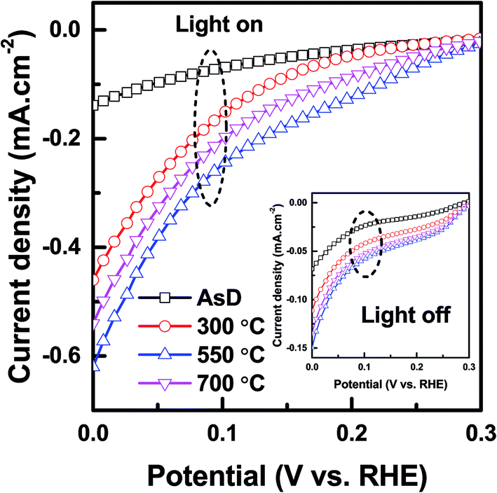 | ||
| Fig. 6 Photoelectrochemical current–voltage measurements for AsD CuO photocathode (200 nm thick) and rapid thermal treated CuO photocathode (200 nm thick) at temperature 300, 550 and 700 °C. | ||
An amperometry analysis is performed at a fixed potential of 0 V vs. RHE as presented in Fig. 7. As shown at this figure increasing the annealing temperature up to 550 °C improves the photocurrent of the prepared samples, while further increase in the annealing temperature degrades the photocurrent of the prepared samples. The stability of the prepared sample also follows the same trend as that of photocurrent. The AsD sample could retain 40% of the initial photocurrent while the sample annealed at 550 °C could retain 65% of the initial current. By further increasing the annealing temperature to the 700 °C the stability of the sample degrades and it could retain only 45% of the initial photocurrent. The AsD film has minimum photocurrent and lowest stability due to poor crystalline quality. Separation of photo generated electron and its transportation from the CuO to the FTO as well as separation of photo generated holes towards electrolytes directly influence the photocurrent and its stability. Indeed, the improvement of crystallinity facilitates the generation and separation of large numbers of long-lived e−/h+ pairs in the CuO thin film that are then transported to their respective electrodes. This increases charge transfer significantly, which promotes the photocurrent and stability of PEC water splitting. Annealing increases the average grain size and hence the grains boundaries area over a given distance decreases. This results in a decrement of the trapped carriers in the grain boundary and reduction of grain boundary scattering which leads to a higher amount of free carriers and improved carrier diffusion length and ultimately results in the enhancement of carrier concentration and improvement of the photocurrent of the CuO film. Grain boundaries also act as photocorrosion centers51 and consequently influence the stability of the prepared samples. The enhanced photocurrent and improved stability in 550 °C treated films is mainly attributed to the reduction of e−/h+ pair recombination due to optimized crystallinity. By further increase in annealing temperature to 700 °C the reduction of photocurrent and its stability despite the enhancement of crystallinity and grain size of the prepared thin film, might be because of the degradation of conductivity of FTO coated substrate at very high annealing temperature of 700 °C.
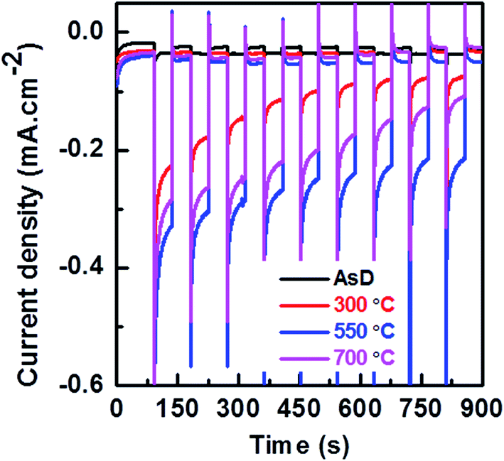 | ||
| Fig. 7 Photocurrent stability test using amperometry measurements of AsD CuO films (200 nm thick) and rapid thermal treated CuO films (200 nm thick) at 300, 550 and 700 °C for 15 min time duration under visible light ON/OFF conditions. | ||
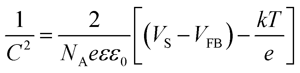
The kinetics of interfacial charge transfer of the CuO electrodes are investigated using electrochemical impedance spectroscopy through Mott–Schottky (MS) plot. MS equation is described by:22
 | (4) |
 | ||
| Fig. 8 (a) Electrochemical Mott–Schottky plot of as-deposited and heat treated CuO photocathodes (200 nm thick) and (b) Nyquist plot of AsD and heat treated CuO films (200 nm thick) at 300, 550 and 700 °C. | ||
The electrochemical impedance spectra (EIS) of AsD and annealed CuO thin films (300, 550 and 700 °C) under standard solar light illumination at a potential of 0 V vs. RHE were compared in Fig. 8b. The semicircle feature of Nyquist plot at high frequencies is attributed to the charge transfer process where the diameter of the semicircle is equal to the charge transfer resistance (Rct).22 It is clear from Nyquist plot that the Rct is significantly reduced with increasing annealing temperature. Rct of the prepared samples were tabulated in Table 1. The reduction of Rct is mainly attributed to the faster carrier transfer rate and better separation efficiency of photo induce charges, resulting from densification of the film due to increase in grain size of the samples annealed at higher temperatures. Since the densification of the samples reduces the recombination rate via efficient transport of charge carriers (e− and h+), it significantly enhances the migration of generated electrons and holes to the surface of the CuO and hence improves the Rct and promote the interfacial charge transport. These results indicate that the kinetics at the electrode–electrolyte interface is controlled by charge transfer resistance which is significantly influenced by crystal quality and grain size of the sputtered films.
| AsD | 300 °C | 550 °C | 700 °C | |
|---|---|---|---|---|
| R ct (kΩ cm2) | 139.5 | 93.4 | 68.8 | 41.5 |
The enhancement of carrier concentration and reduction of Rct is mainly responsible for faster carrier transfer rate, due to improvement in crystallinity and densification of the film. Since the densification of the samples reduces the recombination rate via efficient transport of charge carriers (e− and h+), it significantly enhances the migration of generated electrons and holes to the surface of the CuO and hence improves the Rct. The enhancement of carrier concentration might also be ascribed to the fact that the trap probability of interstitial Cu is increased by increasing annealing temperature, resulting in efficient intrinsic doping.
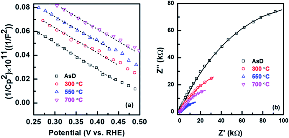
Thickness of CuO layer significantly influences the light absorption and charge carrier transport properties. Therefore, it is also necessary to evaluate its influence on the performance of CuO based PEC water splitting. In Fig. 9 the PEC current–voltage and stability characteristics of the CuO thin film with thicknesses ranging from 200 to 700 nm were illustrated. When thickness of CuO is increased from 200 to 550 nm the value of photocurrent is also increased simultaneously. However, further increase in CuO thickness to 700 nm results in a degradation of the photocurrent. The initial enhancement of photocurrent is mainly attributed to improvement in light absorption capabilities of the thicker CuO film. However, carrier recombination also increases with the thickness of the film.52 Thus, the optimum thickness obtained is ∼550 nm which produces 1.68 mA cm−2 photocurrent at 0 V vs. RHE. The influence of CuO absorber layer on the stability of sputtered film is also demonstrated in Fig. 9b. Thicker CuO film results in a slightly more stable photocurrent. The 700 nm CuO film could retain 70% of its initial photocurrent which is slightly better than the 67% achieved by the 200 nm film.
 | ||
| Fig. 9 (a) Photoelectrochemical current–voltage measurements and (b) photocurrent stability test of sputter grown CuO photocathode with thicknesses ranging from 200 to 700 nm. All CuO photocathodes was rapid thermal annealed at 550 °C in nitrogen ambient for 1 min before PEC test. | ||
Conclusion
In summary, the crystallinity and grain size of the CuO thin film are significantly influenced by annealing temperature. Optimization of these parameters effectively improved the stability and photocurrent of CuO photocathode. We found that increase in annealing temperature decrease the grains boundary area over a given distance and significantly improve photocatalytic water splitting due to reduction of grain boundary scattering and recombination rates. Electrochemical impedance spectroscopy analyses also revealed larger grain size enhances the interfacial charge transfer. With the increased in CuO film thickness to 550 nm, the photocurrent density increased to 1.68 mA cm−2 at 0 V vs. RHE, giving the highest photocurrent performance compared to 200, 400 and 700 nm thick CuO photocathode under optimum annealing condition. Although the sample annealed at 700 °C had the highest crystallinity and grain size, the sample annealed at 550 °C exhibited the highest PEC water splitting performance due to the degradation of the conducting substrate which is detrimental toward the charge transport.References
- C. Wadia, A. P. Alivisatos and D. M. Kammen, Environ. Sci. Technol., 2009, 43, 2072–2077 CrossRef CAS PubMed.
- J. Brillet, J.-H. Yum, M. Cornuz, T. Hisatomi, R. Solarska, J. Augustynski, M. Graetzel and K. Sivula, Nat. Photonics, 2012, 6, 824–828 CrossRef CAS.
- M. G. Kibria, F. A. Chowdhury, S. Zhao, B. AlOtaibi, M. L. Trudeau, H. Guo and Z. Mi, Nat. Commun., 2015, 6, 6797 CrossRef CAS PubMed.
- J.-W. Jang, C. Du, Y. Ye, Y. Lin, X. Yao, J. Thorne, E. Liu, G. McMahon, J. Zhu, A. Javey, J. Guo and D. Wang, Nat. Commun., 2015, 6, 7447 CrossRef PubMed.
- I. S. Cho, C. H. Lee, Y. Feng, M. Logar, P. M. Rao, L. Cai, D. R. Kim, R. Sinclair and X. Zheng, Nat. Commun., 2013, 4, 1723 CrossRef PubMed.
- A. Paracchino, V. Laporte, K. Sivula, M. Grätzel and E. Thimsen, Nat. Mater., 2011, 10, 456–461 CrossRef CAS PubMed.
- C. G. Morales-Guio, S. D. Tilley, H. Vrubel, M. Gratzel and X. Hu, Nat. Commun., 2015, 5, 3059 Search PubMed.
- Y.-F. Lim, C. S. Chua, C. J. J. Lee and D. Chi, Phys. Chem. Chem. Phys., 2014, 16, 25928–25934 RSC.
- C. Liu, N. P. Dasgupta and P. Yang, Chem. Mater., 2014, 26, 415–422 CrossRef CAS.
- M. Long, R. Beranek, W. Cai and H. Kisch, Electrochim. Acta, 2008, 53, 462–4626 CrossRef.
- C.-Y. Chiang, Y. Shin and S. Ehrman, Energy Procedia, 2014, 61, 1799–1802 CrossRef CAS.
- L. Chen, S. Shet, H. Tang, H. Wang, T. Deutsch, Y. Yan, J. Turner and M. Al-Jassim, J. Mater. Chem., 2010, 20, 6962–6967 RSC.
- H. Tang, M. A. Matin, H. Wang, S. Sudhkar, L. Chen, M. M. Al-Jassim and Y. Yan, J. Electron. Mater., 2012, 41, 3062–3067 CrossRef.
- C.-Y. Chiang, J. Epstein, A. Brown, J. N. Munday, J. N. Culver and S. Ehrman, Nano Lett., 2012, 12, 6005–6011 CrossRef CAS PubMed.
- C.-Y. Chiang, Y. Shin, K. Aroh and S. Ehrman, Int. J. Hydrogen Energy, 2012, 37, 8232–8239 CrossRef CAS.
- C.-Y. Chiang, Y. Shin and S. Ehrman, J. Electrochem. Soc., 2012, 159, B227–B231 CrossRef CAS.
- C.-Y. Chiang, K. Aroh, N. Franson, V. R. Satsangi, S. Dass and S. Ehrman, Int. J. Hydrogen Energy, 2011, 36, 15519–15526 CrossRef CAS.
- S. Masudy-Panah, R. S. Moakhar, C. S. Chua, H. R. Tan, T. I. Wong, D. Chi and G. K. Dalapati, ACS Appl. Mater. Interfaces, 2016, 8(2), 1206–1213 CAS.
- Y. Liu, J. Shi, Q. Peng and Y. Li, Chem.–Eur. J., 2013, 19, 4319–4326 CrossRef CAS PubMed.
- A. A. Dubale, C.-J. Pan, A. G. Tamirat, H.-M. Chen, W.-N. Su, C.-H. Chen, J. Rick, D. W. Ayele, B. A. Aragaw, J.-F. Lee, Y.-W. Yang and B.-J. Hwang, J. Mater. Chem. A, 2015, 3, 12482–12499 CAS.
- A. Kargar, Y. Jing, S. J. Kim, C. T. Riley, X. Pan and D. Wang, ACS Nano, 2013, 7, 11112–11120 CrossRef CAS PubMed.
- J. Han, X. Zong, X. Zhoua and C. Li, RSC Adv., 2015, 5, 10790–10794 RSC.
- Z. H. Zhang and P. Wang, J. Mater. Chem., 2012, 22, 2456–2464 RSC.
- P. Wang, Y. H. Ng and R. Amal, Nanoscale, 2013, 5, 2952–2958 RSC.
- P. Wang, X. Wen, R. Amal and Y. H. Ng, RSC Adv., 2015, 5, 5231–5236 RSC.
- Z. Liu, H. Bai, S. Xu and D. D. Sun, Int. J. Hydrogen Energy, 2011, 36, 13473–13480 CrossRef CAS.
- X. Zhao, P. Wang and B. Li, Chem. Commun., 2010, 46, 6768–6770 RSC.
- Q. Huang, F. Kang, H. Liu, Q. Li and X. Xiao, J. Mater. Chem. A, 2013, 1, 2418–2425 CAS.
- Q. Simon, D. Barreca, A. Gasparotto, C. Maccato, T. Montini, V. Gombac, P. Fornasiero, O. I. Lebedev, S. Turner and G. V. Tendeloo, J. Mater. Chem., 2012, 22, 11739–11747 RSC.
- V. Figueiredo, E. Elangovan, G. Gonçalves, P. Barquinha, L. Pereira, N. Franco, E. Alves, R. Martins and E. Fortunato, Appl. Surf. Sci., 2008, 254, 3949–3954 CrossRef CAS.
- S. P. Meshram, P. V. Adhyapak, U. P. Mulik and D. P. Amalnerkar, Chem. Eng. J., 2012, 204–206, 158–168 CrossRef CAS.
- S. Masudy-Panah, G. K. Dalapati, K. Radhakrishnan, A. Kumar, H. R. Tan, E. N. Kumar, C. Vijila, C. C. Tan and D. Chi, Prog. Photovoltaics, 2015, 23, 637–645 CAS.
- S. Masudy-Panah, K. Radhakrishnan, H. R. Tan, R. Yi, T. I. Wong and G. K. Dalapati, Sol. Energy Mater. Sol. Cells, 2015, 140, 266–274 CrossRef CAS.
- S. Masudy-Panah, G. K. Dalapati, A. Kumar, K. Radhakrishnan and H. R. Tan, J. Appl. Phys., 2014, 116, 074501 CrossRef.
- S. Masudy-Panah, K. Radhakrishnan, A. Kumar, T. I. Wong, R. Yi and G. K. Dalapati, J. Appl. Phys., 2015, 118, 225301 CrossRef.
- G. K. Dalapati, S. Masudy-Panah, S. T. Chua, M. Sharma, T. I. Wong, H. R. Tan and D. Chi, Sci. Rep., 2016, 6, 20182 CrossRef CAS PubMed.
- G. K. Dalapati, S. Masudy-Panah, A. Kumar, C. C. Tan, H. R. Tan and D. Chi, Sci. Rep., 2015, 5, 17810 CrossRef PubMed.
- G. K. Dalapati, S. K. Batabyal, S. Masudy-Panah, Z. Sub, A. Kushwaha, T. I. Wong, H. F. Liu, T. Bhat, A. Iskander, Y.-F. Lim, L. H. Wong, S. Tripathy and D. Chi, Mater. Lett., 2015, 160, 45–50 CrossRef CAS.
- G. K. Dalapati, C. C. Tan, S. Masudy-Panah, H. R. Tan and D. Chi, Mater. Lett., 2015, 159, 455–458 CrossRef CAS.
- S. Masudy-Panah, V. Kumar, C. C. Tan, K. Radhakrishnan and D. Chi, Impact of metal contact on the performance of cupric oxide based thin film solar cells, Proceedings of the IEEE 5th International Nanoelectronics Conference (INEC '13), 2013, pp. 378–380, DOI:10.1109/INEC.2013.6466052.
- V. Kumar, S. Masudy-Panah, C. C. Tan, T. K. S. Wong, D. Chi and G. K. DalapatiCopper oxide based low cost thin film solar cells, Proceedings of the IEEE 5th International Nanoelectronics Conference (INEC '13), 2013, pp. 443–445, DOI:10.1109/inec.2013.6466072.
- H. Liu, H. Lu, L. Zhang and Z. Wang, Nucl. Instrum. Methods Phys. Res., 2015, 360, 60–63 CrossRef CAS.
- J. Chrzanowski and J. C. Irwin, Solid State Commun., 1989, 70, 11–14 CrossRef CAS.
- V. Hayez, J. Guillaume, A. Hubin and H. Terryn, J. Raman Spectrosc., 2004, 35, 732–738 CrossRef CAS.
- L. Debbichi, M. C. Marco de Lucas, J. F. Pierson and P. Krüger, J. Phys. Chem. C, 2012, 116(18), 10232–10237 CAS.
- J. F. Xu, W. Ji, Z. X. Shen, W. S. Li, S. H. Tang, X. R. Ye, D. Z. Jia and X. Q. Xin, J. Raman Spectrosc., 1999, 30, 413–415 CrossRef CAS.
- A. F. Khan, M. Mehmood, S. K. Durrani, M. L. Alie and N. A. Rahim, Structural and optoelectronic properties of nanostructured TiO2 thin films with annealing, Mater. Sci. Semicond. Process., 2015, 29, 161–169 CrossRef CAS.
- G. K. Dalapati, R. S. Kajen, S. Masudy-Panah and P. Sonar, J. Phys. D: Appl. Phys., 2015, 48, 495104 CrossRef.
- D. Gao, J. Zhang, J. Zhu, J. Qi, Z. Zhang, W. Sui, H. Shi and D. Xue, Nanoscale Res. Lett., 2010, 5, 769–772 CrossRef CAS PubMed.
- Z. Wang, Y. Liu, D. J. Martin, W. Wang, J. Tang and W. Huang, Phys. Chem. Chem. Phys., 2013, 15, 14956–14960 RSC.
- T. Wang, Z. Luo, C. Li and J. Gong, Chem. Soc. Rev., 2014, 43, 7469–7484 RSC.
- C.-Y. Chiang, K. Aroh and S. H. Ehrman, Int. J. Hydrogen Energy, 2012, 37, 4871–4879 CrossRef CAS.
Footnote |
| † Electronic supplementary information (ESI) available. See DOI: 10.1039/c6ra03383k |
| This journal is © The Royal Society of Chemistry 2016 |