Improving the photoelectrocatalytic performance of boron-modified TiO2/Ti sol–gel-based electrodes for glycerol oxidation under visible illumination

Federico J. Mancillaa, Silvia F. Rojasa, Andrés F. Gualdrón-Reyes*a, María I. Carreño-Lizcanoa, Liseth J. Duartea and M. E. Niño-Gómezab
aCentro de Investigaciones en Catálisis – CICAT, Universidad Industrial de Santander, km 2 vía El Refugio, C.P. 681011, Piedecuesta, Santander, Colombia. E-mail: andresgualdron105@gmail.com
bCentro de Materiales y Nanociencias (CMN), Universidad Industrial de Santander, km 2 vía El Refugio, C.P. 681011, Piedecuesta, Santander, Colombia

Received 30th January 2016 , Accepted 28th April 2016

First published on 29th April 2016


Abstract

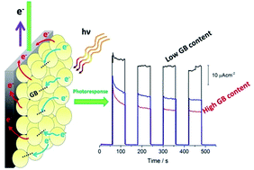
The effect of preparation variables such as the amount of water, the number of layers and the heating rate on the photoelectrocatalytic properties of boron-modified TiO2 sol–gel thin films was investigated. Materials were prepared by the sol–gel method and the deposition of a B-TiO2 film on Ti substrates by the dip-coating technique. The surface and chemical environment of the films was characterized by FESEM, DRS, XPS, and Raman spectroscopy and their photoelectrochemical properties were studied by voltammetry and photocurrent transient measurements under visible light. FESEM micrographs exhibit a cracked surface as a result of the increase of the capillary pressure in the films during drying to increase the number of layers. The Raman spectra show that the anatase phase was obtained during thermal treatment at 450 °C. Films employed as photoelectrodes in a three-electrode cell generated a higher photocurrent than the TiO2 film without modification did due to the presence of boron, which favors the formation of Ti3+ donor states identified by XPS, photogenerating more electrons in the semiconductor and promoting their transport to the substrate. The donor state density was estimated by Mott–Schottky plots. The highest photoresponse was obtained using a one-layer B-TiO2 film. In the presence of 1 M glycerol at pH 1, the photocurrent generated by the B-TiO2 films was increased about twice compared with the photocurrent observed in the absence of the organic, as a result of electron injection to the conduction band of TiO2 from the molecule during its oxidation in the film/electrolyte solution interface, promoting the current doubling effect.


1. Introduction

Advanced oxidation processes are widely studied in the removal of pollutants in wastewater, emphasizing the photocatalysis (PC), which is environmentally friendly due to the use of non-toxic materials such as TiO2 with a high oxidant power under illumination, and other features such as high thermal and chemical stability and low cost.1 However, the recombination of photogenerated charge carriers (electron–hole pairs) is induced during light absorption from the semiconductor, which decreases the photoactivity of the material and hinders the oxidation of organic compounds. Furthermore, the use of TiO2 suspensions favors loss and fouling of the material, hindering its reuse.2 To overcome these disadvantages, TiO2-based thin films have been supported on conducting substrates to be employed as electrodes in photoelectrocatalysis, where an external potential is applied to transport the photogenerated electrons from the TiO2 film/solution interface to the substrate, inhibiting the electron–hole pair recombination and generating a high photocurrent.3 This effect induces accumulation of the photogenerated holes in the semiconductor, enhancing its photoactivity with respect to the PC process.3,4 The preparation of electrodes from sol solutions and their deposition by the dip-coating technique allows homogeneous and uniform material surfaces with high adherence to the substrate to be obtained, compared with some deposition methods such as spray-drying, chemical vapor deposition and the use of suspension-based films, which exhibit detachment from the substrate.5,6

Although the photoelectrocatalysis enhances the photoactivity of TiO2, high energy illumination such as UV light is required to active the semiconductor, which limits its performance in the oxidation of pollutants. Therefore, alternatives such as TiO2 modification with metal and non-metal atoms such as Ag, Fe, N, C, and S,7–11 have been incorporated in the semiconductor preparation. These impurities can extend the spectral region of TiO2 to the low energy regions such as visible, facilitating its photoactivation and increasing its photoelectrocatalytic (PEC) performance. More recently in a previous work,12 boron was incorporated in TiO2/graphene sol–gel films deposited on 304 stainless steel, generating a high photoresponse during the PEC phenol oxidation, which was 30 times higher than that of a TiO2 film without modification. In this case, graphene (rGO) was added in order to improve the electron flow into the photoelectrodes. However, the contribution of rGO on the photoactivity of the materials was not considerable due to the electron transport problems in the film/substrate interface, generating a low photocurrent compared with the response reported for TiO2 films deposited on other conducting substrates (e.g. titanium and ITO).13,14 Hence, the preparation of films on high conductivity substrates is fundamental to promote efficient electron transport in the photoelectrodes and thereby obtain a high performance of the semiconductor. On the other hand, the preparation variables of films such as the amount of the precursors, heating rates, and obtaining multilayers have been also studied to see their effect on the microstructure, morphology and stability.15 However, few reports have mentioned their influence on the photoactivity of these materials.

Hence, the effect of the amount of water in the sol precursor, the number of layers and the heating rate during the thermal treatment on the PEC properties of TiO2 thin films modified with 0.028 wt% boron and deposited on Ti substrates by the dip-coating technique was studied. The PEC performance of the films used as photoelectrodes was observed through the photoresponse generated during glycerol oxidation under visible light illumination.

2. Experimental

Titanium butoxide (Ti-(n-OC4H9)4, 97%) and acetylacetone (CH3COCH2COCH3, 99.3%) were purchased from Aldrich, while boric acid (H3BO3, 99.5%) and anhydrous ethanol (99.5%) were obtained from Merck. All solutions used in the experimentation were prepared with Mili-pore water (18 MΩ cm−1).

B-TiO2 (BT) films were prepared according to the procedure mentioned in a previous work.12 Briefly, Ti(n-OC4H9)4 was added to a solution containing CH3COCH2COCH3, anhydrous ethanol and 0.2 wt/v% H3BO3 (0.028 wt/v% boron) under vigorous stirring during 1 h. The Ti(n-OC4H9)4[thin space (1/6-em)]:[thin space (1/6-em)]CH3COCH2COCH3 molar ratio was 1.0[thin space (1/6-em)]:[thin space (1/6-em)]0.5. Subsequently, water was added in different amounts (0.3 mL, 0.7 mL and 1.1 mL) into the solution. Yellow stable sols were obtained. Titanium plates of 5 cm2 were polished with no. 120, 240, 320 and 600 SiC emery papers. Plates were cleaned using an ultrasonic bath with ethanol and acetone. The BT films were deposited from sol solutions by the dip-coating technique at a rate of 60 mm min−1, followed by dehydration at 100 °C and calcination at 450 °C with constant heating rates of 1, 3 and 5 °C min−1, holding for 90 min. The deposition and drying steps were repeated 1, 2 and 3 times in order to prepare films with different thicknesses. The materials are denominated as X-BT-S, where X is the amount of water contained in the sol, while S is the heating rate used during calcination of the film. Raman spectra of materials were obtained on a Horiba Lab Ram HR with an excitation wavelength of 532 nm. The laser beam was focused onto the samples by means of a 100× objective, while the laser power density was 10 mW. The surface of films was established by field emission scanning electron microscopy (FESEM) employing a JOEL Quanta 650 FEG equipped with EDAX Apollo X energy dispersive X-ray spectroscopy (EDS). The band gap of the films was estimated by diffuse reflectance spectroscopy (DRS), which was recorded with a Shimadzu PC 2401 UV-vis spectrophotometer using a titanium plate as a reference in the range of 200–800 nm.

X-ray photoelectron spectra were obtained for the 0.7-BT-3 film using a Kratos Axis Ultra spectrometer (Kratos Analytical, Manchester, UK) equipped with a monochromatized aluminum X-ray source, powered at 10 mA and 15 kV. The pressure in the analysis chamber was about 1 × 10⁻⁶ Pa. The 0.7-BT-3 film was sputter-cleaned using an argon ion beam rastered over an area of 2 mm × 2 mm to remove carbon contamination and improve the boron signal. The analyzed area was 700 μm × 300 μm. The pass energy of hemispherical analyzer was set at 160 eV for the wide scan and 40 eV for narrow scans. Charge stabilization was achieved using the Kratos Axis device. The following sequence of spectra was recorded: survey spectrum, C 1s, O 1s, B 1s, Ti 2p and C 1s again to check for charge stability as a function of the time and for absence of degradation of the sample during the analyses. The binding energy (BE) values were referred to as the C–(C,H) contribution of the C 1s peak fixed at 284.8 eV. Data treatment was performed with the Casa XPS program (Casa Software Ltd., UK) and the spectra were decomposed using a Gaussian/Lorentzian (70/30) product function, with the FWHM of the peak components kept identical.

The BT films used as photoelectrodes were electrochemically analyzed in a three-electrode cell with a potentiostat AUTOLAB PGSTAT 302N. A Ag/AgCl electrode in a Luggin capillary was used as the reference electrode, while a graphite rod (99.9995% pure, Alfa Aesar) was employed as the counter electrode. The open circuit potential (OCP) was measured irradiating the films in solution with visible light and exposing to illumination for 13 min once. Linear sweep voltammograms were obtained in duplicate with a scan rate of 10 mV s−1 using 0.1 M HClO4 (60%, Panreac) as the support electrolyte, in the presence and absence of 1 M glycerol which was bubbled with nitrogen during 20 min in order to ensure that the dissolved oxygen was removed. The solution volume was 60 mL. Chopped light voltammograms were acquired with switch-on and switch-off of the illumination during 10 cycles. Photocurrent transient measurements were performed under an applied potential of 0.85 V during four light on/off cycles. All the electrochemical measurements were carried out with and without illumination using a MHN-TD Phillips metal halide lamp (150 W, UV-block) with a light intensity of 60 mW cm−2. Mott–Schottky plots were obtained to determinate the donor state density and the flatband for the films after boron modification. The measurements were performed in a solution containing 0.1 M HClO4 under dark conditions, at a signal amplitude and frequency of 10 mV and 400 Hz, respectively. The potential window was −0.3 to 0.8 V in the cathodic direction with a sweep rate of 20 mV s−1. The geometric area of the X-BT-S photoelectrodes exposed during the measurements was 3 cm2.

3. Results and discussion

3.1. Morphology, optical properties and chemical environment of films

Fig. 1 shows the typical micrographs of BT films prepared from sol solutions with 0.7 mL of water, calcined at 450 °C using a heating rate of 3 °C min−1, varying the number of layer films (0.7-BT-3).
image file: c6ra02806c-f1.tif
Fig. 1 FESEM images of (a) one, (b) two and (c) three-layer 0.7-BT-3 films (5000×). Effect of the amount of water in the X-BT-3 films, X: (d) 0.3 mL, and (e) 1.1 mL. Varying the heating rate during calcination for the 0.7-BT-S films, S: (f) 1 °C min−1, and (g) 5 °C min−1. Corresponding magnifications (a′–g′) at 150[thin space (1/6-em)]000×.

On observing the morphology of one (Fig. 1a), two (Fig. 1b), and three (Fig. 1c) layer films, the latter exhibits more cracks in its surface compared with the other films, due to the increase in the capillary pressure during solvent evaporation.15 To deposit a sol–gel film, it is concentrated and adhered on the substrate by evaporation, promoting tensile stress in the liquid which is balanced with the compressive stress from the metallic support.16 In this stage, the evaporation of alcohol is induced, favoring the water enrichment during the hydrolysis and the condensation processes of the titanium alkoxide precursor, increasing the capillary pressure of the film as a result of the high surface tension of water.15,16 From Fig. 1a′–c′, the average thickness values for the one, two and three-layer 0.7-BT-3 films was estimated to be 130.9 nm, 202.2 nm and 244.7 nm, respectively, indicating that the three-layer film will contain a higher amount of water, which means a high tensile stress over the substrate and thereby a highly warped and cracked surface. In addition, EDS spectra (Fig. 1Sa–c, ESI) were obtained for each film, confirming the presence of Ti, O, C and B. Hence, one-layer BT films were chosen to carry out the electrochemical characterization discussed below, presenting fewer cracks to generate a high photoresponse.

The effect of the amount of water contained in the BT sol solutions was also considered. The one-layer BT films deposited from sols with 0.3 mL (0.3-BT-3) and 1.1 mL (1.1-BT-3) of water show a less uniform surface compared with that of the 0.7-BT-3 film (Fig. 1a), due to the polished lines formed during the treatment of the substrate, which are concentrators of the sol (Fig. 1d and e). Therefore, the average thicknesses of the 0.3-BT-3 and 1.1-BT-3 films were determined to be 144.4 nm (Fig. 1d′) and 143.3 nm (Fig. 1e′), respectively, which were higher than that of the 0.7-BT-3 film. In addition, light zones can be evidenced in the surface of the 1.1-BT-3 film due to the presence of TiO2 aggregates. To add a high amount of water in a sol, the aging of the solution is accelerated, causing an increase in the particle size and sometimes the precipitation of TiO2.15 In this context, to increase the amount of water at 1.1 mL in the BT sol, the fast hydrolysis and condensation of titanium alkoxide could be promoted, inducing the formation of agglomerates on the film surface. The effect of the heating rate on the surface of the BT films was also exhibited. Comparing again with the 0.7-BT-3 film (Fig. 1a), the BT films calcined at 1 °C min−1 and 5 °C min−1 (0.7-BT-1 and 0.7-BT-5, respectively) also show less uniformity by the polished lines, as well as presenting TiO2 agglomerates (Fig. 1f and g). It indicates that the fast or low solvent evaporation during thermal treatment does not promote appreciable changes in the morphology of the material. However, a rough surface can retain more sol during its deposition and induce the formation of TiO2 aggregates. The average thickness values were recorded to be 150 nm (Fig. 1f′) and 119.8 nm (Fig. 1g′) for the 0.7-BT-1 and 0.7-BT-5 films, respectively. The decrease of thickness can be attributed to favoring of the film densification, which retards the nucleation of particles during thermal treatment.17

The crystalline phase of the 0.7-BT-3 films with different numbers of layers after the thermal treatment at 450 °C was observed by Raman spectroscopy (Fig. 2a). The spectra exhibit five characteristic signals at 140.7 cm−1 (Eg), 181.3 cm−1 (Eg), 393.4 cm−1 (B1g), 515.4 cm−1 (A1g) and 636.3 cm−1 (Eg), attributed to the anatase phase.9 The peak at 320.6 cm−1 is associated to the titanium substrate, whose spectrum is also shown (Fig. 2a). The intensities of the two and three-layer BT films were decreased ×3 and ×7 respectively, for comparative purposes. For a one-layer BT film, the signal ascribed to the substrate was also identified, indicating that the substrate was coated by a thin film. Nevertheless, this peak was decreased to increase the number of BT layer films, hindering the detection of the metallic support. On the other hand, Fig. 2b shows the modified Kubelka–Munk function employed to estimate the band gap of the one-layer TiO2 and BT films. The band gap values were 2.93 eV and 2.53 eV for the TiO2 and 0.7-BT-3 films, respectively. Therefore, boron diminishes the photoactivation energy of the films, extending the light absorption of the semiconductor to the visible region. The decrease in the band gap value has been attributed to the presence of impurity levels below the conduction band (CB) of TiO2.18,19


image file: c6ra02806c-f2.tif
Fig. 2 (a) Raman spectra of 0.7-BT-3 films with different numbers of layers and (b) Kubelka–Munk approach to estimate the band gap of the TiO2 and 0.7-BT-3 films.

Fig. 3 exhibits the XPS analysis performed on the one-layer 0.7-BT-3 film in order to observe its chemical environment and composition. In the wide scan spectrum of the BT film (Fig. 3a), the presence of B, C, O and Ti was confirmed. The binding energy (BE) of the elements was estimated by fixing the component associated to the adventitious carbon (C–(C,H)) at 284.8 eV as the reference. Subsequently, the high-resolution spectra for each element were determined to identify the species present in the material. Fig. 3b shows the core level XPS B 1s spectrum for the BT film, which was composed of 3 contributions: 191.9 eV, 192.9 eV and 193.7 eV. The two latter BEs are commonly associated with a B–O–B-type bond due to the presence of boron species formed after the thermal treatment as boric oxide (B2O3) taking into account that the standard B 1s BE for the compound is between 192 and 194 eV.19–21 Dai et al.21 mentioned that the co-existence of this signals indicates the formation of B2O3 into or at the surface of the TiO2 structure.


image file: c6ra02806c-f3.tif
Fig. 3 XPS wide scan spectrum (a) and high-resolution spectra of (b) C 1s, (c) B 1s and (d) Ti 2p for the 0.7-BT-3 film.

The signal at 191.9 eV is evidence of the existence of boron in interstitial positions forming a B–O–Ti-type bond into TiO2. Finazzi et al.22 mentioned that interstitial boron can promote the reduction of Ti4+ to form Ti3+, which are considered as donor states below the CB of the semiconductor. Thus, the spectral response of TiO2 to the visible region can be enhanced.

On the other hand, the high-resolution C 1s spectrum of the BT film is exhibited in Fig. 3b. The peak was decomposed into four contributions at 284.8 eV, 286.3 eV, 287.8 eV and 289.3 eV. The first signal was associated to the adventitious carbon C–(C,H), while the second contribution was ascribed to the carbon singly bound to the oxygen atoms (C–O). The third and fourth signals were attributed to the O–C–O and O[double bond, length as m-dash]C–O species.23,24 In the core level XPS O 1s spectrum (Fig. 2S, ESI), the carbon–oxygen species were also observed at 531.4 eV and 532.8 eV, taking into account the representative signal associated to oxygen from the TiO2 lattice (Ti–O) at 530.1 eV. The obtained XPS C 1s spectrum is typical for the adventitious carbon added to the film before performing the XPS analysis.23 The high-resolution Ti 2p spectrum for the BT film is also shown (Fig. 3d), exhibiting three contributions attributed to titanium species, Ti2+, Ti3+, and Ti4+. For Ti2+, the peaks are located at 455.5 eV (Ti 2p3/2) and 461 eV (Ti 2p1/2). For Ti3+, Ti 2p3/2 is located at 456.9 eV and Ti 2p1/2 at 462.7 eV and for Ti4+, Ti 2p3/2 and Ti 2p1/2 are located at 458.7 eV and 464.4 eV respectively.25 The XPS Ti 2p spectrum was also obtained for a non-modified TiO2 film for comparative purposes. After boron modification, an increase of the component associated to Ti3+ besides a decrease in the Ti4+ species was evidenced. The presence of Ti3+ implies boron incorporation in interstitial positions forming a B–O–Ti-type bond within the TiO2 lattice without modifying its structure.19,26 In this way, a direct correlation between the boron doping and the formation of Ti3+ species can be appreciated. The presence of Ti2+ in the spectrum indicates the possible reduction of Ti species during Ar+ bombardment.

3.2. Photoelectrochemical properties of X-BT-S films

Fig. 4a shows the OCP measurements performed in 0.1 M HClO4 for the 0.7-BT-3 films used as photoelectrodes, to obtain information about their photoactivity under visible light. During the illumination of the photoelectrode, the electron–hole pairs are photogenerated in the semiconductor, where the holes are accumulated in the valence band (VB) and migrate to the semiconductor/electrolyte interface to react with the electrolyte.3 In the absence of reducing agents such as inorganic and organic molecules, the holes are consumed by the water molecules to generate hydroxyl radicals, promoting the accumulation of electrons in the CB of the material and causing a displacement in the OCP value to more negative potentials.12,27
image file: c6ra02806c-f4.tif
Fig. 4 Effect of the number of layers on (a) the open circuit potential, (b) linear voltammetry and (c) photocurrent transient measurements (0.85 V) performed in 0.1 M HClO4 for (i and iv) one, (ii) two and (iii) three-layer 0.7-BT-3 films under visible light and dark conditions. (d) Representation of electron transport in the BT films depending on the thickness.

In this case, the electrochemical potential of the electrons in the solid, also denominated as the Fermi level is increased to reach a quasi-Fermi level. It is well known that the Fermi level of a metal is lower than the Fermi level of the semiconductor,28 therefore, when the TiO2 film is in contact with the titanium substrate, the electrons accumulated in the semiconductor are transferred via the CB until the Fermi level of the metal and TiO2 are equal, favoring the special separation of the charge carriers. Then, a photostationary stage is reached. To interrupt the illumination, the OCP value is slowly returned to the initial value in the dark as a result of the emptying of different energy levels below the CB of the semiconductor.27 When recording the OCP of one, two and three-layer BT films (Fig. 4ai–iii), the materials are photoactive in the visible region, showing a decrease in the OCP value. However, the latter film presented the highest OCP displacement. To show a thicker film on Ti according to the FESEM images, the three-layer BT film-based photoelectrode contained more available material for the photoactivation, photogenerating more electrons and thereby obtaining a high photoresponse.

During the photogeneration of charge carriers in photocatalysis, the oxidant power of the semiconductor is limited by the electron–hole recombination, decreasing the available holes in the photoelectrode to perform oxidation processes. In order to promote the charge carrier separation in the material, the photogenerated electrons are transported out to the photoelectrode through an applied potential, while the holes are accumulated in the semiconductor to improve its oxidative performance. The PEC process is useful to observe the electron transport in the material as a response of its conductivity, besides the increase in its photoactivity.12 Thus, the PEC behavior of the BT films used as photoelectrodes in 0.1 M HClO4 was observed through voltammetry measurements (Fig. 4b). Under illumination, the OCP values of the films were displaced to a more negative potential than the value obtained in dark conditions, indicating the accumulation of electrons in the material attributed to the n-type semiconductivity of the BT films. On sweeping the applied potential from the OCP to 1.5 V, a photocurrent is produced (Fig. 4bi–iii) and it is higher than the current obtained in the dark (Fig. 4biv). The photoresponse is evidence of photogenerated electron transport from the film/electrolyte solution interface to the metallic support and its posterior mobility to the external circuit of the cell, ensuring the spatial separation of charge carriers.

On the other hand, the generated photocurrent decreases on increasing the thickness of the films in the following order: one-layer > two-layers > three-layer BT films. Villarreal et al.29 mentioned that for a nanoparticle TiO2-based photoelectrode, monoenergetic states such as grain boundaries (GBs) are presented in the material. These states act as recombination centers where the electrons are accumulated, hindering their transport and thereby decreasing the photocurrent (Fig. 3S, ESI). As it is shown in Fig. 4d, to increase the thickness of the BT-based photoelectrodes, more GB states are contained in the semiconductor, providing a tortuous way for the electrons to reach the titanium substrate. In order to corroborate the photoresponse observed in the linear voltammograms for each film, photocurrent transient measurements were performed at 0.85 V, in 0.1 M HClO4 during 10 min, carried out for four on/off light cycles (Fig. 4c). On applying a positive enough potential, the charge carrier separation is favored, inducing the electron mobility in the photoelectrode and causing a rapid increment in the photocurrent. The one-layer 0.7-BT-3 film presents the highest photoresponse as a result of efficient electron–hole pair separation and electron transport. A high GB state content inhibits the electron mobility, which also promotes the charge carrier recombination, impacting negatively on the photocurrent generation. From the OCP and voltammetry analysis, it is relevant to mention that although a photoelectrode shows a high photocatalytic performance, this does not mean that it is efficient in photoelectrocatalysis, demonstrating the difference of both processes.

Varying the amount of water in the sol precursor and the heating rate employed during the thermal treatment also affected the PEC properties of the X-BT-S films. As a result of a high sol content on the substrate and the formation of TiO2 aggregates, the 0.3-BT-3, 1.1-BT-3 and 0.7-BT-1 films show a thicker surface compared with that of the 0.7-BT-3 film, where more GB states can be contained, hindering the electron transport in the photoelectrode and diminishing the photocurrent (Fig. 5a–d). In contrast, the 0.7-BT-5 film (Fig. 5d) presents a smaller thickness after the densification process, representing a greater facility in the electron transport. However, a low photocurrent was generated during the PEC measurements compared with the 0.7-BT-3 film, due to less material being available to the illumination, dcreasing the charge carrier photogeneration. Comparing with a one-layer TiO2 film without modification (Fig. 5e), the one-layer 0.7-BT-3 film exhibits a higher photocurrent which was 7.2 times greater (Fig. 5f), indicating that more electrons are available to be transported to the titanium substrate. The photogenerated electrons are promoted from the Ti3+ donor states formed by boron modification, identified during the XPS analysis. On the other hand, using the 0.7-BT-3 film for the oxidation of a model molecule as glycerol, a higher photocurrent was generated (Fig. 5g) and it was approximately twice that compared with the photoresponse obtained in the absence of organics. At pH 1, the photogenerated holes oxidize water molecules to produce hydroxyl radicals. However, in the presence of glycerol, the holes can directly interact with the organic, promoting the formation of radical intermediates which are stabilized by liberating and injecting one electron to the CB of TiO2.30 It can be observed in the shift of the onset potential (photocurrent equal to zero) to more negative values in comparison with the measurement in the absence of organics due to the increase of electrons accumulated in the photoelectrode. Therefore, the effect where one electron is transferred to the semiconductor during oxidation of the organic molecule and one electron is injected during the intermediate stabilization is commonly known as current doubling. The effect of glycerol on the generation of current doubling has been recently studied in PEC cells under alkaline media using ethanol as a hole scavenger, hindering glycerol to react with holes in the photoelectrode/electrolyte interface and promoting its oxidation by hydroxyl radicals.30,31 However, under acidic conditions, the oxidation of glycerol by holes can be facilitated.


image file: c6ra02806c-f5.tif
Fig. 5 Linear voltammograms obtained in 0.1 M HClO4 in the absence of 1 M glycerol for the one-layer (a) 0.3-BT-3, (b) 1.1-BT-3, (c) 0.7-BT-1, (d) 0.7-BT-5, (e) non-modified TiO2, and (f) (duplicated) 0.7-BT-3 film-based photoelectrodes, and (g) in the presence of the organic compound for the 0.7-BT-3 film.

In order to observe the enhanced PEC performance and stability of the 0.7-BT-3 film, the oxidation of a more complex molecule was carried out. Gentamicin (VITALIS injectable antibiotic, INVIMA 2004M-0003994) was chosen due to the fact that this aminoglycoside is considered as an emerging pollutant in wastewater, promoting the formation of bacteria with high antibiotic resistance. Chopped light voltammograms were obtained in 0.1 M HClO4, in the presence and absence of 1 mM of antibiotic during 10 switch-on/off cycles using the same photoelectrode (Fig. 6). An increase of the photocurrent compared with the photoresponse obtained in the absence of Gentamicin was evidenced, confirming first, the continuous photoactivation of the material during the switch-on/off cycles and second, the high oxidant power of the photoelectrode for the degradation of organic pollutants.


image file: c6ra02806c-f6.tif
Fig. 6 Chopped light voltammograms obtained in 0.1 M HClO4 for the 0.7-BT-3 film-based photoelectrode during 10 switch-on/off cycles in (a) the absence and (b) the presence of 1 mM Gentamicin.

3.3. Semiconducting behavior of the photoelectrodes

According to the enhancement in the photoresponse for the one-layer 0.7-BT-3 film, the Mott–Schottky curves (Fig. 7) were obtained with the purpose of analyzing the ability of the photoelectrode to promote the electron transport as a result of the change in the semiconducting properties after boron modification, described by the flatband potential (Efb) and the charge carrier density (Nd). The measurements were carried out in 0.1 M HClO4 as the support electrolyte under dark conditions. Efb and Nd were estimated employing the following relationship:27
 
image file: c6ra02806c-t1.tif(1)
where q is the elementary charge (+e for electrons), ε is the relative permittivity of the semiconductor (TiO2, ε = 86), ε0 is the vacuum permittivity, A is the exposed geometric area of the photoelectrode, k is the Boltzmann constant, T is the absolute temperature and Csc2 is the capacitance of the space charge.32 Efb is obtained from the intercept with the potential axis. During the potential sweep in the cathodic direction, a linear region with positive slopes was observed for the non-modified TiO2 and BT-based photoelectrodes, indicating their n-type semiconductivity, previously determined in the OCP measurements. However, the slope of the linear region of the 0.7-BT-3 film (Fig. 7b) was lower compared with that of the TiO2 film (Fig. 7a), indicating an increase of the charge carrier density after boron modification (Table 1). Taking into account the XPS analysis, the Ti3+ species content was also increased after the boron incorporation, corroborating the formation of donor states in the material. This explains the improvement of the conductivity in the photoelectrode, which promotes the photogenerated electron mobility. Efb was also displaced to more negative potentials increasing the donor states in the 0.7-BT-3 film due to more electrons being accumulated in the semiconductor, which causes a closing of the Fermi level to the CB of TiO2.33 This shift indicates a higher band bending of TiO2, establishing a facilitated charge carrier separation in the photoelectrode/electrolyte interface.

image file: c6ra02806c-f7.tif
Fig. 7 Mott–Schottky plots performed in 0.1 M HClO4 under dark conditions for (a) the one-layer non-modified TiO2 and (b) the one-layer 0.7-BT-3 films.
Table 1 Mott–Schottky parameters estimated for the one-layer TiO2 and one-layer 0.7-BT-3 films
Photoelectrode MS parameters
Nd × 1020 (cm−3) Efb (V vs. Ag/AgCl, 3 M KCl)
TiO2 0.33 −0.12
0.7-BT-3 1.60 −0.21


3.4. Photoactivation mechanism of B-TiO2 and electron mobility in a PEC cell

Fig. 8 summarizes the photoactivation of an n-type TiO2-based photoelectrode after boron modification. According to the band gap values estimated from the modified Kubelka–Munk function (Fig. 2b), TiO2 can be photoactivated with an energy of 2.93 eV to photogenerate charge carriers. However, the presence of boron in interstitial positions into the TiO2 shifts the light absorption to lower energy values in the visible region, requiring now a band gap of 2.53 eV. This red-displacement is the result of the formation of Ti3+ species after the reduction of Ti4+ in the photoelectrode, which is to 0.4 eV from the CB of TiO2. Thus, the electrons promoted to the Ti3+ states from the VB of the semiconductor can be excited to the CB, enhancing the charge carrier separation.34 Taking into account that the electron mobility is facilitated for a one-layer BT film, the photogenerated electrons are transported to the Ti substrate and the external circuit of the cell to be collected by the cathode to generate molecular hydrogen.35 The holes are accumulated in the photoelectrode to carry out the oxidation of organic compounds. In the case of glycerol at pH 1, holes directly react with the organic to produce intermediates which stabilize injecting one electron to the CB of TiO2, increasing the photoresponse by the current doubling effect. An increase of the thickness in the photoelectrode induces the electron trapping by GB states, decreasing the charge carrier separation and thereby the oxidant power of the photoelectrode.
image file: c6ra02806c-f8.tif
Fig. 8 Schematic representation of the BT-based photoelectrode photoactivation in a PEC cell under visible illumination.

4. Conclusions

X-BT-S film-based photoelectrodes were successfully prepared by the sol–gel method and deposited on Ti substrates by the dip-coating technique, evidencing an improvement in the photoelectrocatalytic response to employ a one-layer film from a BT sol with 0.7 mL of water, and calcined at a heating rate of 3 °C min−1. The generated photocurrent was 7.2 times compared with that of a TiO2 film without modification. The presence of boron in the TiO2 lattice extends the light absorption of the semiconductor to the visible region due to the formation of Ti3+ donor states below the CB of TiO2, also increasing the electron accumulation in the film to generate a high photoresponse. On the other hand, to increase the number of layers and vary the amount of water and the heating rate during the preparation of the films, more GB states are formed in the semiconductor, restraining the transport of electrons photogenerated under illumination, decreasing the PEC performance of the materials. In the presence of an organic compound such as glycerol under acidic conditions, the photocurrent generated for the 0.7-BT-3 film was increased about twice due to the oxidation of a molecule in the film/electrolyte interface, transferring two electrons to the photoelectrode, inducing the current doubling effect.

Acknowledgements

This work was financially supported by Universidad Industrial de Santander (VIE project 1339 and Colciencias project 8836). Andrés F. Gualdrón and María I. Carreño gratefully acknowledge COLCIENCIAS for the Ph.D grant through the Doctorado Nacional Colciencias conv. 617 and 647 programs. To Carlos Chacón and Carolina Mendoza from Laboratorio de Microscopia PTG-102 for FESEM images. To prof. Ángel M. Meléndez from Laboratorio de Electroquímica PTG-304 for the photoelectrochemistry supports, and P. Eloy From Université Catholique de Louvain-IMCN for the XPS analysis support.

References

  1. Q. Ling, J. Sun and Q. Zhou, Appl. Surf. Sci., 2008, 254, 3236 CrossRef CAS.
  2. J. Yu and X. Zhao, Mater. Res. Bull., 2000, 35, 1293 CrossRef CAS.
  3. H. Gerischer, Electrochim. Acta, 1990, 35, 1677 CrossRef CAS.
  4. J. Y. Shi, W. H. Leng, W. C. Zhu, J. Q. Zhang and C. N. Cao, Chem. Eng. Technol., 2006, 29, 146 CrossRef CAS.
  5. Y. Liu, D. Zhang, Y. Shang, W. Zang and M. Li, RSC Adv., 2015, 5, 104785 RSC.
  6. J. Altmayer, S. Barth and S. Mathur, RSC Adv., 2013, 3, 11234 RSC.
  7. N. Crespo-Monteiro, N. Destouches, L. Saviot, S. Reynaud, T. Epicier, E. Gamet, L. Bois and A. Boukenter, J. Phys. Chem. C, 2012, 116, 26857 CAS.
  8. R. S. Sonawane, B. B. Kale and M. K. Dongare, Mater. Chem. Phys., 2004, 85, 52 CrossRef CAS.
  9. G. Yang, Z. Jiang, H. Shi, T. Xiao and Z. Yan, J. Mater. Chem., 2010, 20, 5301 RSC.
  10. Y. Yang, D. Ni, Y. Yao, Y. Zhong, Y. Ma and J. Yao, RSC Adv., 2015, 5, 93635 RSC.
  11. C. W. Dunnill, Z. A. Aiken, A. Kafizas, J. Pratten, M. Wilson, D. J. Morgan and I. P. Parkin, J. Mater. Chem., 2009, 19, 8747 RSC.
  12. A. F. Gualdrón-Reyes, A. M. Meléndez, M. E. Niño-Gómez, V. Rodríguez-González and M. I. Carreño-Lizcano, Rev. Acad. Colomb. Cienc. Exactas, Fis. Nat., 2015, 39, 77 CrossRef.
  13. Z. Zainal, C. Y. Lee, A. Kassim, M. Z. Hussein and N. A. Yusof, Acta Chim. Slov., 2007, 54, 166 CAS.
  14. P. Wang, Y. Ao, C. Wang, J. Hou and J. Qian, J. Hazard. Mater., 2012, 223–224, 79 CrossRef CAS PubMed.
  15. C. J. Brinker, G. C. Frye, A. J. Hurd and C. S. Ashley, Thin Solid Films, 1991, 201, 97 CrossRef CAS.
  16. C. Jing, X. Zhao and Y. Zhang, Mater. Res. Bull., 2007, 42, 600 CrossRef CAS.
  17. V. Cimalla, M. Baeumler, L. Kirste, M. Prescher, B. Christian, T. Passow, F. Benkhelifa, F. Bernhardt, G. Eichapfel, M. Himmerlich, S. Krischok and J. Pezoldt, J. Mater. Sci. Appl., 2014, 5, 628 CAS.
  18. J. Ding, Y. Yuan, J. Xu, J. Deng and J. Guo, J. Biomed. Nanotechnol., 2009, 5, 7 Search PubMed.
  19. X. Lu, B. Tian, F. Chen and J. Zhang, Thin Solid Films, 2010, 519, 111 CrossRef CAS.
  20. NIST X-ray Photoelectron Spectroscopy Database, version 4.1, National Institute of Standards and Technology, Gaithersburg, MD, 2003, http://srdata.nist.gov/xps/, accessed Dec. 1, 2015 Search PubMed.
  21. H. Tian, L. Hu, C. Zhang, S. Chen, J. Sheng, L. Mo, W. Liu and S. Dai, J. Mater. Chem., 2011, 21, 863 RSC.
  22. E. Finazzi, C. Di Valentin and G. Pacchioni, J. Phys. Chem. C, 2009, 113, 220 CAS.
  23. S. J. Yuan, F. J. Xu, S. O. Pehkonen, Y. P. Ting, E. T. Kang and K. G. Neoh, J. Electrochem. Soc., 2008, 155, C196 CrossRef CAS.
  24. C. D. Wagner, J. F. Moulder, J. E. Davis and W. M. Riggs, Handbook of X-Ray Photoelectron Spectroscopy, Perkin-Elmer Corp., Physical Electronics Division, Eden Prairie, MN, 1992 Search PubMed.
  25. P. Acevedo-Peña, L. Lartundo-Rojas and I. González, J. Solid State Electrochem., 2013, 17, 2939 CrossRef.
  26. C. Di Valentin and G. Pacchioni, Catal. Today, 2013, 206, 12 CrossRef CAS.
  27. D. Ramírez-Ortega, A. M. Meléndez, P. Acevedo-Peña, I. González and R. Arroyo, Electrochim. Acta, 2014, 140, 541 CrossRef.
  28. T. Berger, D. Monllor-Satoca, M. Jankulovska, T. Lana-Villarreal and R. Gómez, ChemPhysChem, 2012, 13, 2824 CrossRef CAS PubMed.
  29. T. Lana-Villarreal, Y. Mao, S. S. Wong and R. Gómez, Nanoscale, 2010, 2, 1690 RSC.
  30. T. Ohno, S. Izumi, K. Fujihara, Y. Masaki and M. Matsumura, J. Phys. Chem. B, 2000, 104, 6801 CrossRef CAS.
  31. E. Kalamaras and P. Lianos, J. Electroanal. Chem., 2015, 751, 37 CrossRef CAS.
  32. K. M. Reddy, S. V. Manorama and A. R. Reddy, Mater. Chem. Phys., 2002, 78, 239 CrossRef.
  33. Q. Kang, J. Cao, Y. Zhang, L. Liu, H. Xu and J. Ye, J. Mater. Chem. A, 2013, 1, 5766 CAS.
  34. J. Georgieva, S. Armyanov, E. Valova, I. Poulios and S. Sotiropoulos, Electrochim. Acta, 2076, 2006, 51 Search PubMed.
  35. P. A. Christensen, T. A. Egerton, S. A. M. Kosa, J. R. Tinlin and K. Scott, J. Appl. Electrochem., 2005, 35, 683 CrossRef CAS.

Footnote

Electronic supplementary information (ESI) available: EDS spectra of one, two and three-layer 0.7-BT-3 film, high-resolution XPS O 1s spectrum of the 0.7-BT-3 film, and grain boundaries generated in the BT photoelectrodes. See DOI: 10.1039/c6ra02806c

This journal is © The Royal Society of Chemistry 2016