Improved performances of inkjet-printed poly(3-hexylthiophene) organic thin-film transistors by inserting an ionic self-assembled monolayer

Yan Lina, Cheng-Fang Liua, Yi-Jing Songa, Lei Yanga, Wen-Jin Zenga, Wen-Yong Lai*ab and Wei Huang*ab
aKey Laboratory for Organic Electronics and Information Displays (KLOEID) & Institute of Advanced Materials (IAM), Jiangsu National Synergetic Innovation Center for Advanced Materials (SICAM), Nanjing University of Posts & Telecommunications, 9 Wenyuan Road, Nanjing 210023, China. E-mail: iamwylai@njupt.edu.cn
bKey Laboratory of Flexible Electronics (KLOFE) & Institute of Advanced Materials (IAM), Jiangsu National Synergetic Innovation Center for Advanced Materials (SICAM), Nanjing Tech University (NanjingTech), 30 South Puzhu Road, Nanjing 211816, China

Received 23rd January 2016 , Accepted 9th April 2016

First published on 14th April 2016


Abstract

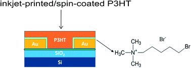
Inkjet printing is a promising technology because of the material conservation and facile patterning compared with other solution-processed techniques, facilitating the scalable fabrication and commercialization of organic electronics. In this study, organic thin-film transistors (OTFTs) based on poly(3-hexylthiophene) (P3HT) by inkjet printing were fabricated and explored by electrical analysis and morphological characterization. By optimizing the processing conditions, the comprehensive performance in terms of the field-effect mobility of inkjet-printed P3HT-based OTFTs was comparable to those of spin-coated P3HT-based OTFTs. More importantly, with the employment of an electrode buffer layer, namely Br(CH2)5N(CH3)3Br, the field-effect mobilities of both spin-coated and inkjet-printed OTFTs were improved in accordance with the expectations, resulting from the reduced contact resistance and improved film quality.


Introduction

Owing to the large-area and low-cost manufacture, solution-processed electronics has attracted much interest for potential applications in organic light-emitting diodes (OLEDs),1 organic thin-film transistors (OTFTs)2,3 and organic photovoltaics (OPVs).4–9 Generally speaking, the most widely used methods for solution-processed devices involve spin coating, screen printing, gravure printing, roll-to-roll printing, and inkjet printing.10–12 Among all these, inkjet printing is one of the most attractive candidates due to specific pattern alignment, template-free deposition and low consumption.13–16 Consequently, much work has been focused on improving the inkjet printing systems through interface control, parameter adjustment and optimization of high-quality films.17,18 Despite recent great advances, most of the high-performance devices based on organic semiconductors via solution processing are still achieved by spin-coating technology.19 Only recently, inkjet-printed OTFTs are reported, but the devices show comparably low mobility and poor on/off ratio.15 According to the literature, relatively high contact resistance is one of the greatest challenges that impede the improvement of the device performance.20–22 In order to address the issue, various strategies have been developed and investigated such as the doping method, electrode modification and the incorporation of a buffer layer between the semiconductor and the electrode.23 Previous studies indicate that molecular doping for OTFTs is mainly accompanied by thermal evaporation, involving too much energy consumption.24 Moreover, the electrode modification by means of plasma has limited influence on decreasing the contact resistance. In contrast, the insertion of a self-assembled monolayer (SAM) between the electrode and the active layer has become an attractive method for reducing the relatively high contact resistance at the organic/metal interface,25 which can be realized via solution processing.26 For example, Chung reported that an appropriate SAM layer was chosen to achieve low contact resistance, further enhancing the charge transport characteristics and device performance.27

Poly(3-hexylthiophene) (P3HT) is one of the most popular polymer semiconductors due to its commercial availability, compatibility with printing processes and the self-assembly property to form polycrystalline structures.28 It is well-documented that the performance of OTFTs based on P3HT heavily relies on the crystallinity of the active layer and the preparation process.29 To date, extensive research towards improving the device performance has been mostly associated with spin-coating, exhibiting variations of the mobilities by several orders of magnitude.30,31 Although inkjet printing has the advantages of pattern alignment, large-area fabrication and low cost, studies about inkjet-printed OTFTs have lagged behind.16,32,33

In this contribution, we fabricated P3HT-based OTFTs by both inkjet printing and spin coating. By optimizing the processing conditions, the device performance of inkjet-printed P3HT was a little lower than that of spin-coated P3HT in terms of the field-effect mobility, but can reach the same order of magnitude. More importantly, an ionic SAM, which consisted of an anchoring group, a linker group, and an ionic functional group as the interfacial layer, was also adopted in the fabrication process to further improve the device performance.25 The field-effect mobility was enhanced by the insertion of Br(CH2)5N(CH3)3Br between the active layer and the electrode.27,34 It is worthwhile to point out that the present case of inkjet-printed P3HT-based OTFTs is an important example for further developing the inkjet printing technology which is not yet mature.29

Experiments

Materials

All chemicals were purchased from Aldrich and J&K and used without further purification. P3HT used in this study had a molecular weight (Mw) of about 50 kDa.

The preparation of P3HT films

As an important organic semiconductor, P3HT is often used as the active layer for OTFTs. The spin coating was performed using a SC100 spin coater. Three kinds of solvents such as chlorobenzene, chloroform, and ortho-dichlorobenzene were tested during the preparation process. In the case of spin-coating, we found that employing ortho-dichlorobenzene as the solvent could not result in a good film. Meanwhile, chloroform was also not a good option because of the low boiling point and rapid evaporation. To optimize the processing conditions, P3HT was dissolved in chlorobenzene at the concentration of 8, 10 and 20 mg mL−1, respectively. The active layers were prepared by spin-coating the solutions at 1000, 2000, 3000 rpm for 60 s. Table 1 summarized the film thicknesses obtained by spin-coating the P3HT solution in chlorobenzene with different concentrations and spin speeds. According to the experimental results, the concentration of 20 mg mL−1 and the speed of 3000 rpm for 60 s were optimal, and the thickness of the corresponding film was about 47 nm. The semiconductor layer's thickness satisfied the requirement of OTFTs. Therefore, the following experiments all adopted this condition.
Table 1 Film thicknesses obtained by spin-coating the P3HT solution in chlorobenzene with different concentrations and spin speeds
  1000 rpm 2000 rpm 3000 rpm
8 mg mL−1 18.5 nm 12 nm 9 nm
10 mg mL−1 29 nm 19 nm 11 nm
20 mg mL−1 78.5 nm 59 nm 47 nm


The inkjet printing was carried out by Dimatix3000 inkjet printer. When chloroform was used as the solvent, the nozzle was clogged, which was not suitable for inkjet printing. Compared with chlorobenzene, ortho-dichlorobenzene with higher viscosity and boiling point proved to be a better solvent to make P3HT suitable for inkjet printing. Based on the test experiments, we selected the optimum condition for printing P3HT ink as ortho-dichlorobenzene with the concentration of 4 mg mL−1. Meanwhile, the viscosity of P3HT ink was measured to be 9.8 cps, which was compatible for inkjet printing. With the aim to ensure the veracity and reliability of the experiment result, we used a nozzle of 10 pL, the print voltage of 30 V, and the ejecting frequency of 2 kHz.

Device fabrication and characterization

As shown in Fig. 1(a), bottom-gate and bottom-contact OTFTs were fabricated on a heavily doped silicon wafer covered with a 300 nm thermal oxidation SiO2 dielectric layer (Ci = 11.5 nF cm−2). After the substrate was cleaned with acetone, ethanol and deionized water sequentially, the surface of SiO2 was modified with octadecyltrichlorosilane (OTS) via vapor deposition. First, the source and drain electrodes (Au: thickness about 40 nm) were fabricated by thermally evaporation with a shadow mask in vacuum at 10−4 Pa. The pattern of interdigital electrodes is depicted in Fig. 1(b). The length (L) and width (W) of the channel were 80 μm and 8800 μm, respectively. Then, P3HT was prepared as thin films by spin coating or inkjet printing. Finally, the transistors were annealed at 70 °C for 1 h in an oven. Moreover, Br(CH2)5N(CH3)3Br was employed to modify the source and drain electrodes to reduce its contact resistance with P3HT. Br(CH2)5N(CH3)3Br was dissolved in 10 mmol ethanol solutions. The ionic SAM as the contact buffer was achieved by immersing the substrate in this solution for 5 min in ambient air and then rinsing with ethanol again. The sheet resistance of Au electrodes before and after ionic SAM treatments was obtained by electrical measurements from 4-probes. All electrical measurements were performed on Keithley 2636 source/measure units at room temperature in air. The field-effect mobilities were extracted from the saturated region of the transfer characteristics.
image file: c6ra02032a-f1.tif
Fig. 1 (a) The schematic diagram of a P3HT-based OFET and the molecular structure of Br(CH2)5N(CH3)3Br. (b) The schematic structure of the interdigitated electrodes used in this study and the W/L was 8800/80.

Results and discussion

In order to fabricate high-performance OTFTs by inkjet printing, high-quality thin films have played a crucial role in the process, requiring optimized conditions. By adjusting the drop spacing can affect the printing dot and the printing line on the surface of SiO2, further resulting in various morphologies and structures of thin films. After inkjet printing, the optical images of P3HT deposited on the prepared surface of SiO2 are shown in Fig. 2, and the drop spacing from left to right is 80 μm, 60 μm, and 40 μm, respectively. Owing to the solvent viscosity problem of P3HT, it is difficult to form a neat point pattern on the surface of SiO2. However, improved thin films of P3HT can be obtained by reducing the drop spacing during the process of inkjet printing. The drop spacing was thus selected as 40 μm, which facilitated a continuous uniform film. Moreover, the optical images of Au electrodes and inkjet-printed P3HT on Au electrodes was shown in Fig. 3 for better visualization.
image file: c6ra02032a-f2.tif
Fig. 2 The optical images of the morphology of P3HT with different drop spacing deposited on SiO2 modified with OTS.

image file: c6ra02032a-f3.tif
Fig. 3 The optical images of (a) Au electrodes and (b) inkjet-printed P3HT on Au electrodes.

As for the device structure of P3HT-based OFET at room temperature, the gold source/drain (S/D) electrodes are formed by evaporation and the corresponding thickness is about 40 nm. The field-effect mobility is calculated based on the following equation in the linear region and saturation region:35

 
image file: c6ra02032a-t1.tif(1)
 
image file: c6ra02032a-t2.tif(2)
where Ci is the capacitance of the gate dielectric; W is the channel width; L is the channel length; Vth is the threshold voltage; and μ is the field effect mobility. The mobility is calculated in the saturation regime by plotting the square root of the drain current versus the gate voltage.

Fig. 4(a) and (b) shows measured transfer and output characteristics of the spin-coated P3HT-based OTFTs. A mobility of 0.001 cm2 V−1 s−1 and an on/off ratio of 103 were extracted from the measured transfer characteristics, which were comparable with those previously reported OTFTs based on P3HT.36,37 For the inkjet-printed P3HT-based OTFTs, a mobility of 0.0008 cm2 V−1 s−1 and an on/off ratio of about 103 were extracted from the measured transfer curves in Fig. 4(c) and (d), which were a little lower compared with those of the spin-coated P3HT-based OTFTs. However, they were almost at the same order of magnitude. That is to say, by means of optimizing the printing conditions, OTFTs using inkjet printing can achieve similar performance to that using spin coating.38


image file: c6ra02032a-f4.tif
Fig. 4 Transfer and output characteristics of (a and b) the spin-coated P3HT-based OTFTs, (c and d) the inkjet-printed P3HT-based OTFTs, (e and f) the spin-coated P3HT-based OTFTs with the Br(CH2)5N(CH3)3Br ionic SAM and (g and h) the ink-jet printed P3HT-based OTFTs with the Br(CH2)5N(CH3)3Br ionic SAM.

To the best of our knowledge, the contact resistance of OTFTs is a major parameter that determines the electrical performance. Br(CH2)5N(CH3)3Br ionic SAM was then chosen as a buffer layer to modify the electrode contact. According to electrical measurements with 4-probes, the sheet resistance of Au electrodes was decreased from 4.7 Ω sq−1 to 3.2 Ω sq−1 with the addition of Br(CH2)5N(CH3)3Br ionic SAM, which indicated reduced contact resistance. As depicted in Fig. 4(e) and (f), transfer and output characteristics of the spin-coated P3HT-based OTFTs with Br(CH2)5N(CH3)3Br ionic SAM exhibited higher mobility than those OTFTs without any treatments. A mobility of 0.06 cm2 V−1 s−1 and an on/off ratio of more than 104 were obtained from the measured transfer characteristics, resulting from the reduction of contact resistance. All devices showed p-type characteristics with clear transitions from linear to saturation behavior, indicating field-effect characteristics. As shown in Fig. 4(f), the saturation current was 1.15 × 10⁻⁵ A at a gate voltage of −50 V, manifesting approximately 5-fold enhancement over that without Br(CH2)5N(CH3)3Br (2.1 × 10⁻⁶ A, Fig. 4(b)). Fig. 4(g) and (h) show the transfer and output characteristics of the inkjet-printed P3HT-based OTFTs with Br(CH2)5N(CH3)3Br ionic SAM, demonstrating higher mobility compared with those without any treatments. In this case, a mobility of 0.002 cm2 V−1 s−1 and an on/off ratio of more than 103 were obtained from the measured transfer characteristics, which was attributed to the relatively low contact resistance. This assumption was confirmed by electrical measurements with 4-probes as revealed above. The average mobility obtained from 12 devices and the corresponding error values are summarized in Table 2. The error is the standard deviation. According to the analysis, owing to the lower contact resistance, OTFTs with ionic SAM treatments exhibited higher mobility than those without any treatments. These results indicated that the device performance in terms of field-effect mobility was improved after the electrode modification with Br(CH2)5N(CH3)3Br ionic SAM for both spin-coated OTFTs and inkjet-printed OTFTs. Consequently, we can draw the conclusion that the treatment with Br(CH2)5N(CH3)3 can reduce the contact resistance between the active layer and the electrode, which is beneficial for improving the device performance.

Table 2 The field-effect mobility of the spin-coated and inkjet-printed OTFTs with and without SAM
  Without SAM With SAM
Spin coating μ (cm2 V−1 s−1) 0.001 ± 0.00042 0.06 ± 0.0021
Inkjet printing μ (cm2 V−1 s−1) 0.0008 ± 0.0001 0.002 ± 0.00022


In order to further investigate the origin of the different device performance, the morphologies of the films were studied by atomic force microscopy (AFM) measurements.39 A close inspection of the AFM images in Fig. 5(a) and (b) revealed that no obvious differences were observed for the spin-coated P3HT films and the inkjet-printed P3HT films. However, the spin-coated P3HT films showed the surface roughness (Ra) of 0.9 nm and the fluctuation (Zmax, which is determined by the deviations between the highest and the lowest values recorded in AFM images) of 6.6 nm, while the inkjet-printed P3HT films showed the surface roughness (Ra = 2.16 nm) and the fluctuation (Zmax = 19.5 nm). This result suggested that the roughness of P3HT films via spin-coating was smaller than that of the inkjet-printed P3HT films, leading to a slightly higher field-effect mobility. By comparison, in Fig. 5(c), the spin-coated P3HT film with modification of Au was smoother (Ra = 0.6 nm, Zmax = 6.2 nm) than those mentioned above, leading to the highest field-effect mobility in our study. Compared with the spin-coated P3HT, inkjet-printed P3HT exhibited coarse films with higher surface roughness (Ra = 1.87 nm) and larger fluctuation (Zmax = 17.4 nm), even after SAM modification. According to the analysis, the field-effect mobility of the resulting devices also correlated with the film quality. Moreover, the insertion of Br(CH2)5N(CH3)3Br ionic SAM enhanced the mobility in both spin-coated and inkjet-printed OTFTs, which could also be probably ascribed to the improved film quality besides the reduced contact resistance as revealed above.


image file: c6ra02032a-f5.tif
Fig. 5 The AFM images of (a) spin-coated P3HT films, (b) inkjet-printed P3HT films and (c) spin-coated P3HT films on Au electrode with the Br(CH2)5N(CH3)3Br ionic SAM. (d) Inkjet-printed P3HT films on Au electrode with the Br(CH2)5N(CH3)3Br ionic SAM. Scan size (5 × 5 μm2).

Conclusions

In summary, P3HT-based OTFTs by ink-jet printing were designed and fabricated in this study, whose field-effect mobility were nearly in the same order of magnitude compared with those by spin coating. However, the mobility of ink-jet printed P3HT-based OTFTs (0.0008 cm2 V−1 s−1) was a little inferior to that of spin-coated P3HT-based OTFTs (0.001 cm2 V−1 s−1), resulting from the relatively coarse morphology. It is worthwhile to mention that a novel material Br(CH2)5N(CH3)3Br ionic SAM layer was applied on the S/D electrode of OTFTs, and the corresponding field-effect mobility was higher than those without modification of the electrode. More specifically, with the SAM layer, OTFTs based on the spin-coated P3HT showed improved mobility up to 0.06 cm2 V−1 s−1 and OTFTs based on the inkjet-printed P3HT exhibited improved mobility up to 0.002 cm2 V−1 s−1. It is concluded that the use of ionic SAM buffer layers is a promising solution to enhance the performance in both spin-coated and inkjet-printed OTFTs, resulting from the low contact resistance and improved film quality. From an application perspective, this study provides useful information to the utilization of inkjet printing technology for the construction of electronic devices, which is beneficial for the rapid advancement in the field of printed electronics.

Acknowledgements

The authors acknowledge financial support from the National Key Basic Research Program of China (973 Program, 2014CB648300), the National Natural Science Foundation of China (21422402, 20904024, 51173081, 61136003), the Natural Science Foundation of Jiangsu Province (BK20140060, BK20130037, BM2012010), Program for Jiangsu Specially-Appointed Professors (RK030STP15001), Program for New Century Excellent Talents in University (NCET-13-0872), Specialized Research Fund for the Doctoral Program of Higher Education (20133223110008, and 20113223110005), the Synergetic Innovation Center for Organic Electronics and Information Displays, the Priority Academic Program Development of Jiangsu Higher Education Institutions (PAPD), the NUPT “1311 Project”, the Six Talent Plan (2012XCL035), the 333 Project (BRA2015374) and the Qing Lan Project of Jiangsu Province.

References

  1. S. T. Han, Y. Zhou, Z. X. Xu and V. Roy, Appl. Phys. Lett., 2012, 101(3), 033306 CrossRef.
  2. Y. D. Jiang, T. H. Jen and S. A. Chen, Appl. Phys. Lett., 2012, 100(2), 023304 CrossRef.
  3. Z. Liu, J. Zhao, W. Xu, L. Qian, S. Nie and Z. Cui, ACS Appl. Mater. Interfaces, 2014, 6(13), 9997–10004 CAS.
  4. W. Huang, H. Zhang, J. Ma, M. Chen, H. Zhu and W. Wang, J. Mater. Chem. C, 2015, 24(3), 6200–6208 RSC.
  5. F. C. Krebs, T. Tromholt and M. Jørgensen, Nanoscale, 2010, 2(6), 873–886 RSC.
  6. M. Helgesen, R. Søndergaard and F. C. Krebs, J. Mater. Chem., 2010, 20(1), 36–60 RSC.
  7. R. Søndergaard, M. Hösel, D. Angmo, T. T. Larsen-Olsen and F. C. Krebs, Mater. Today, 2012, 15(1), 36–49 CrossRef.
  8. F. C. Krebs, Sol. Energy Mater. Sol. Cells, 2009, 93(4), 394–412 CrossRef CAS.
  9. A. Bruno, F. Villani, I. A. Grimaldi, F. Loffredo, P. Morvillo, R. Diana and C. Minarini, Thin Solid Films, 2014, 560, 14–19 CrossRef CAS.
  10. T. Cheng, Y. Z. Zhang, W. Y. Lai and W. Huang, Adv. Mater., 2015, 27(22), 3349–3376 CrossRef CAS PubMed.
  11. Z. Stempien, E. Rybicki, T. Rybicki and J. Lesnikowski, Sens. Actuators, B, 2016, 224, 714–725 CrossRef CAS.
  12. H. Kim, J. I. Jang, H. H. Kim, G. W. Lee, J. A. Lim, J. T. Han and K. Cho, ACS Appl. Mater. Interfaces, 2016, 8(5), 3193–3199 CAS.
  13. Z. Zhang, X. Zhang, Z. Xin, M. Deng, Y. Wen and Y. Song, Adv. Mater., 2013, 25(46), 6714–6718 CrossRef CAS PubMed.
  14. S. H. Ko, H. Pan, C. P. Grigoropoulos, C. K. Luscombe, J. M. Fréchet and D. Poulikakos, Nanotechnology, 2007, 18(34), 345202 CrossRef.
  15. S. Chung, S. O. Kim, S. K. Kwon, C. Lee and Y. Hong, IEEE Electron Device Lett., 2011, 32(8), 1134–1136 CrossRef CAS.
  16. S. Chung, M. Jang, S. B. Ji, H. Im, N. Seong, J. Ha, S. K. Kwon, Y. H. Kim, H. Yang and Y. Hong, Adv. Mater., 2013, 25(34), 4773–4777 CrossRef CAS PubMed.
  17. M. Kuang, L. Wang and Y. Song, Adv. Mater., 2014, 26(40), 6950–6958 CrossRef CAS PubMed.
  18. L. Zhang, D. Yang, Y. Wang, H. Wang, T. Song, C. Fu and B. Zou, IEEE Photonics Technol. Lett., 2015, 27(14), 1535–1538 CrossRef.
  19. S. P. Tiwari, K. A Knauer, A. Dindar and B. Kippelen, Org. Electron., 2012, 13(1), 18–22 CrossRef CAS.
  20. H. Hu and R. G. Larson, J. Phys. Chem. B, 2006, 110(14), 7090–7094 CrossRef CAS PubMed.
  21. M. Strecker, J. Brill, S. Köhler, R. T. Weitz and N. Fruehauf, Phys. Status Solidi A, 2015, 212(8), 1634–1642 CrossRef CAS.
  22. A. Khaliq, F. L. Xue and K. Varahramyan, Microelectron. Eng., 2009, 86(11), 2312–2315 CrossRef CAS.
  23. W. Huang, W.-L. Yu, H. Meng, J. Pei and S. F. Y. Li, Chem. Mater., 1998, 10(11), 3340–3345 CrossRef CAS.
  24. R. Liu, F. Shen, H. Ding, J. Lin, W. Gu, Z. Cui and T. Zhang, J. Micromech. Microeng., 2013, 23(6), 065027 CrossRef.
  25. L. Zhao, D. Cao, Z. Gao, B. Mi and W. Huang, Chin. J. Chem., 2015, 33(8), 828–841 CrossRef CAS.
  26. D. Kim, L. Zhu, D. J. Jeong, K. Chun, Y. Y. Bang, S. R. Kim, J. H. Kim and S. K. Oh, Carbon, 2013, 63, 530–536 CrossRef CAS.
  27. J. Lee, J. S. Park, B. L. Lee, J. i. Park, J. W. Chung and S. Lee, Org. Electron., 2014, 15(9), 2021–2026 CrossRef CAS.
  28. W. Shi, J. Yu, W. Huang, X. Yu and Y. Zheng, Appl. Phys. Lett., 2013, 102(11), 111607 CrossRef.
  29. T. Kushida, T. Nagase and H. Naito, Org. Electron., 2010, 11(7), 1323–1326 CrossRef CAS.
  30. S. Tiwari, W. Takashima, S. K. Balasubramanian, S. Miyajima, S. Nagamatsu, S. S. Pandey and R. Prakash, Jpn. J. Appl. Phys., 2014, 53(2), 021601 CrossRef.
  31. L. Zhang, D. Yang, S. Yang and B. Zou, Appl. Phys. A: Mater. Sci. Process., 2014, 116(3), 1511–1516 CrossRef CAS.
  32. D. Kwak, J. A. Lim, B. Kang, W. H. Lee and K. Cho, Adv. Funct. Mater., 2013, 23(42), 5224–5231 CrossRef CAS.
  33. A. Määttänen, P. Ihalainen, R. Bollström, M. Toivakka and J. Peltonen, Colloids Surf., A, 2010, 367(1), 76–84 CrossRef.
  34. J. Doggart, Y. Wu, P. Liu and S. Zhu, ACS Appl. Mater. Interfaces, 2010, 2(8), 2189–2192 CAS.
  35. Y. Guo, G. Yu and Y. Liu, Adv. Mater., 2010, 22(40), 4427–4447 CrossRef CAS PubMed.
  36. S. Kim, B. Kang, M. Lee, S. G. Lee, K. Cho, H. Yang and Y. D. Park, RSC Adv., 2014, 4(77), 41159–41163 RSC.
  37. D. Khim, K. J. Baeg, B. K. Yu, S. J. Kang, M. Kang, Z. Chen and Y. Y. Noh, J. Mater. Chem. C, 2013, 1(7), 1500–1506 RSC.
  38. K. J. Baeg, D. Khim, J. Kim, H. Han, S. W. Jung, T. W. Kim and Y. Y. Noh, ACS Appl. Mater. Interfaces, 2012, 4(11), 6176–6184 CAS.
  39. J. Jeong, M. Kim, S.-H. Lee, D. Kim, T. Kim and Y. Hong, IEEE Electron Device Lett., 2011, 32(12), 1758–1760 CrossRef CAS.

This journal is © The Royal Society of Chemistry 2016
Click here to see how this site uses Cookies. View our privacy policy here.