
Facile synthesis of ZnPc nanoflakes for cold cathode emission
Madhupriya Samanta†
a,
Uttam Kumar Ghorai†a,
Biswajit Dasa,
Promita Howlib,
Swati Dasb,
Dipayan Senb and
Kalyan Kumar Chattopadhyay*ab
aSchool of Materials Science and Nanotechnology, Jadavpur University, Kolkata 700 032, India. E-mail: kalyan_chattopadhyay@yahoo.com; Fax: +91 33 2414 6007; Tel: +91 33 2413 8917
bThin Film & Nanoscience Laboratory, Department of Physics, Jadavpur University, Kolkata 700 032, India
First published on 18th April 2016
Abstract
The challenge of developing two dimensional metal phthalocyanine nanostructures by controlling the reaction protocols is successfully addressed in the present work by synthesizing zinc phthalocyanine (ZnPc) novel nanoflakes using a simple low temperature hydrothermal route. The as synthesized samples were characterized by X-ray diffraction (XRD), Fourier transform infrared spectroscopy (FTIR), ultra-violet visible spectrometer (UV-Vis), X-ray photoelectron spectroscopy (XPS) and field emission scanning electron microscope (FESEM). The field emission or cold cathode emission characteristics of these phthalocyanine nanostructures have been reported for the first time here and it is shown that as prepared nanoflakes can act as electron field emitter having a turn-on field 4.7 V μm−1 at a current density of 1 μA cm−2 for an inter electrode distance of 130 μm. The local electric field distributions around nanoflakes were also further studied theoretically using a finite element method. The obtained results indicate that ZnPc nanoflakes are the potential candidate for electron emission based applications such as vacuum nanoelectronic devices and field emission display devices.
Introduction
In the last few decades, organic semiconductors have gained significant interest due to its various applications such as non-volatile memory devices, solar cells, light emitting diodes, field effect transistors etc.1–5 The low temperature deposition technique, mechanically flexible nature and light weight for the processing of the organic nanostructures are advantageous over the inorganic and other counterparts.6,7 Among the organic semiconductors, metal phthalocyanines (MPcs), consisting of central metallic atom bound to a π conjugated ligand, are of special interest because of their high molecular symmetry, electron delocalization, high thermal, chemical stability and outstanding optical and electronic properties.8–11 Field induced electron emission properties of these phthalocyanine nanostructures as well as organic nanostructures have garnered an incredible thrust for the development of field emission display (FED) where electrons are emitted from these nanostructures by overcoming surface potential barrier in the presence of an externally applied electric field. Recently we have reported the cold cathode emission property of copper phthalocyanine (CuPc) nanostructures such as CuPc nanowires, nanotubes, nanotips and CuPc nanoparticles functionalized amorphous carbon nanotube.12–15 In these regards, field emission properties of other kinds of organic nanostructures such as Cu-TCNAQ (tetracyanoanthraquinodimethane) nanowires, CuTCNQ (tetracyanoquinodimethane) nanotubes, CuTCNQ nanorods, aligned PANI nanotubes, Alq3 {Tris(8-hydroxyquinoline)aluminium} nanowires, FePc, H2Pc, CuPc nanowires and nanofibers are well documented in literatures.16–24 To the best of the authors' knowledge, there is no report related to field emission property of any kind of zinc phthalocyanine (ZnPc) nanostructures.Various methods are employed to the synthesis of ZnPc nanostructures. For example, Tong et al.25 fabricated the ZnPc nanoribbon through organic vapour phase deposition. ZnPc nanoflower with aggregated nanoparticle on gold coated quartz substrates was synthesized by Karan et al.26 through vapour deposition techniques. Chowdhury et al.27 prepared the ZnPc nanorods by thermal evaporation method followed by post annealing technique. All the methods require high temperature and special kind of templates for the development of ZnPc nanostructures. Therefore alternative approaches such as self assembly, hydrothermal and solvothermal are advantageous techniques over the physical deposition routes. Guo et al.28 reported the ZnPc hierarchical nanostructure with hollow interior space by solvothermal route and studied their photocatalytic property. Till now there is no report in the literatures on the synthesis of novel ZnPc nanoflakes through hydrothermal route.
In this work, the authors report the fabrication of ZnPc nanoflakes through hydrothermal route. The chemical structure, phase purity, exact valence state and morphology were analysed by Fourier transform infrared spectroscopy (FTIR), X-ray diffraction (XRD) technique, X-ray photoelectron spectroscopy (XPS) and field emission scanning electron microscopy (FESEM) respectively. Field emission properties of the synthesized nanostructures are reported here. Additionally finite element method is used to justify the experimental results from theoretical point of view.
Experimental
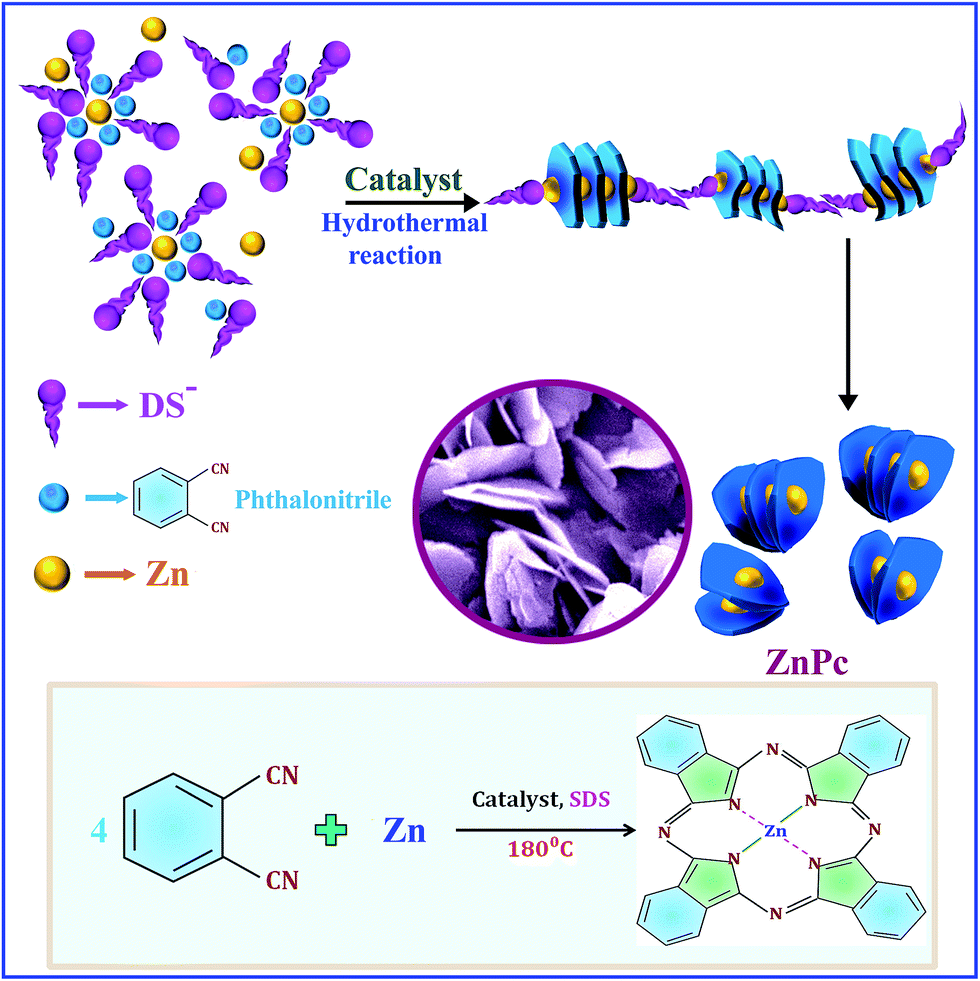
Zinc phthalocyanine (ZnPc) nanoflakes were formed through a simple low temperature hydrothermal route in water at 180 °C. In a typical reaction, zinc powder (0.45 mmol), phthalonitrile (1.8 mmol), sodium dodecyl sulphate (SDS) (20 mg) and ammonium molybdate (10 mg) were dispersed in water (12 ml) and the solution was vigorously stirred for 40 minutes. After that the resulting solution was put in a Teflon lined stainless-steel auto clave (15 ml volume) and kept at 180 °C temperature for 24 h. Finally the blue-purple precipitate was washed with 1 (M) HCl aqueous solution, ethanol and water separately and then dried at 60 °C for over night.The as-prepared samples were characterized by X-ray diffraction technique (XRD-Rigaku Ultima-III, by Cu Kα radiation and λ = 1.54059 Å). In this measurement, the sample was put on a quartz substrate and 2θ ranging from 5° to 30° with scanning rate 2° min−1. The chemical structure of the synthesized nanoflakes was analysed by the help of Fourier transform infrared (FTIR) spectrometer (Shimadzu IRPrestige-21, spectral resolution 0.5 cm−1). X-ray photoelectron spectroscopy (SPECS, HSA 3500) was used to examine the valence states of the constituent elements in the sample where monochromatic Al Kα with hν = 1486.6 eV was used as X-ray source. Morphological study of the as prepared sample was carried out by field emission scanning electron microscope (FESEM, Hitachi S-4800). Field emission studies were measured in high vacuum field emission set up.
Results and discussion
The crystallinity of the as-prepared ZnPc nanoflakes was analyzed by XRD analysis. The major peaks of ZnPc were obtained at 6.86°, 9.14°, 10.5°, 12.51°, 18.16°, 18.68°, 21.16°, 23.66°, 26.18°, 28.06° values of 2θ, which corresponds to reflection from (![[1 with combining macron]](https://www.rsc.org/images/entities/char_0031_0304.gif) 01), (101), (002), (200), (
01), (101), (002), (200), (![[3 with combining macron]](https://www.rsc.org/images/entities/char_0033_0304.gif) 01), (202), (12), (211), (212), (311), (13) plane of ZnPc respectively which is shown in the Fig. 1(a). All the peaks are well suited with standard JCPDS data card (number: 39-1882).29 The chemical structure of ZnPc nanoflakes was analysed by Fourier transformed IR spectra shown in the Fig. 1(b). The peaks at 726 cm−1 and 777 cm−1 were assigned to the C–H out of plane deformation and the peaks at 753 cm−1, 1085 cm−1, 1118 cm−1, 1167 cm−1, 1286 cm−1 corresponds to C–H in plane bending. The peaks at 889 cm−1 and 1411 cm−1 are assigned to isoindole stretching. The peaks at 1060 cm−1, 1332 cm−1 and 1486 cm−1 are related to C–H bending, in-plane pyrrole stretching and C
01), (202), (12), (211), (212), (311), (13) plane of ZnPc respectively which is shown in the Fig. 1(a). All the peaks are well suited with standard JCPDS data card (number: 39-1882).29 The chemical structure of ZnPc nanoflakes was analysed by Fourier transformed IR spectra shown in the Fig. 1(b). The peaks at 726 cm−1 and 777 cm−1 were assigned to the C–H out of plane deformation and the peaks at 753 cm−1, 1085 cm−1, 1118 cm−1, 1167 cm−1, 1286 cm−1 corresponds to C–H in plane bending. The peaks at 889 cm−1 and 1411 cm−1 are assigned to isoindole stretching. The peaks at 1060 cm−1, 1332 cm−1 and 1486 cm−1 are related to C–H bending, in-plane pyrrole stretching and C![[double bond, length as m-dash]](https://www.rsc.org/images/entities/char_e001.gif) C benzene stretching respectively.11,30 X-ray spectroscopy technique is used to confirm the exact valence state of the constitute elements present in the ZnPc nanoflakes. The peak located in the Fig. 1(c) shows the core level spectra of Zn 2p and have two spin–orbit split components which are positioned at 1022.5 eV and 1045.6 eV of the electronics states of Zn 2p3/2 and 2p1/2 respectively.9,31 The Fig. 1(d) shows the high resolution spectrum of N 1s at 394.5 to 403.0 eV, consisting of two groups of nitrogen atoms in dissimilar chemical environments in the ZnPc.31
C benzene stretching respectively.11,30 X-ray spectroscopy technique is used to confirm the exact valence state of the constitute elements present in the ZnPc nanoflakes. The peak located in the Fig. 1(c) shows the core level spectra of Zn 2p and have two spin–orbit split components which are positioned at 1022.5 eV and 1045.6 eV of the electronics states of Zn 2p3/2 and 2p1/2 respectively.9,31 The Fig. 1(d) shows the high resolution spectrum of N 1s at 394.5 to 403.0 eV, consisting of two groups of nitrogen atoms in dissimilar chemical environments in the ZnPc.31
 | ||
| Fig. 1 (a) XRD pattern of ZnPc nanoflakes; (b) FTIR spectra of ZnPc nanoflakes; (c) & (d) high resolution spectra of Zn 2p doublet and N 1s respectively. | ||
Fig. 2 shows the UV-Vis absorption spectrum of ZnPc nanoflakes. The absorption band from 300 to 450 nm corresponds to B band arising from the deeper π levels to LUMO transition and the band 550 nm to 750 nm implies the Q-absorption band of ZnPc. In the Q band, the peaks observed at 604 nm and 667 nm are mainly due to the π–π* transition of monomer from the HOMO state to the LUMO state of the Pc2− ring. The peak is found at 637 nm in the Q band which might be responsible for the vibronic band due to the dimers and multimers.28
 | ||
| Fig. 2 UV-Vis spectra of ZnPc nanoflakes. | ||
The FESEM images of the as synthesized ZnPc nanostructures at different magnifications are shown in the Fig. 3. In the Fig. 3(a) and (b) some nanoflakes are interconnected with each other. The diameters of the nanoflakes are around 700 nm and thicknesses of the nanoflakes are 20–40 nm. Fig. 3(d) shows the commercially available potatochips which is similar to our hydrothermally synthesized nanostructures. That's why our synthesized nanoflakes can be called as nanochips. It is clearly shown that the sharp edges are present in the single nanoflake periphery (shown in the Fig. 3(c)) which helps to produce the local field enhancement and field emission. A schematic growth mechanism for nanoflakes formation is shown in the Fig. 4. In the reaction, ammonium molybdate acts as a catalyst to accelerate the hydrothermal reaction and at first small nuclei are formed and after that these small nuclei tend to grow the 2d sheet like morphology in the presence of surfactant at 180 °C.
 | ||
| Fig. 3 (a)–(c) FESEM images of ZnPc nanoflakes at different magnifications; (d) digital image of commercially available chips. | ||
 | ||
| Fig. 4 Schematic formation process of ZnPc nanoflakes. | ||
In the present work, SDS behaves as structure-directing agent and in the solution, SDS decomposes into DS− (C12H25–O–S–O3−) and Na+ ion in water medium which pretentious the morphology of the hydrothermally derived nanostructures. At the initial stage of reaction, small ZnPc nuclei are formed where zinc powders acts as the nucleating agent and SDS provides the microenvironment for the synthesis of ZnPc.6 When temperature increases, it tends to form one dimensional nanostructure through along c-axis due to its monoclinic unit cell. But DS− ions were anchored with the Zn2+ ions of ZnPc structure due to the electrostatic attraction of anions and cations.32,33 This adsorption of DS− ions blocked the further nucleation and growth of self-assembly process through π–π and van der Waals interaction for the formation of 1D phthalocyanine nanostructure. This soft templating behaviour of SDS in the solution phase profoundly modifies the final 2 dimensional nanoflake like structures34 which are clearly seen in the Fig. 3(c). Another important role of SDS is that SDS acts as an emulsifying agent in the solution phase to provide a hydrophobic environment and hydrolysis of phthalonitrile precursor is prevented by this microenvironment.6 When the temperature increases and reaches at 180 °C, surface tension of the system decreases and this reduced surface tension help to lower the aggregation behaviours and form the well resolved nanosheet like morphology. Same kinds of observations are found elsewhere.35,36
Cold cathode emission characteristics were performed in our home designed high vacuum system at pressure of ∼10−6 mbar. High vacuum is achieved by using diffusion pump with a liquid nitrogen trap and high vacuum level was measured through a penning gauge. In our experiment, samples glued onto a conducting carbon tape that acted as cathode and a conical shaped stainless steel tip (1.0 mm tip diameter) worked as anode. From macroscopic point of view, it seems conical shaped; however, the bottom of the tip has a flat, smooth circular surface of 1 mm diameter. Thus in nano regime, the anode behaves like a flat plate and a parallel plate configuration is obtained. So, uniform electric field is generated. The electric field was determined from the ratio of applied voltage with the separation distance. The sample size was ∼10 mm × 10 mm and the anode–cathode distance was adjustable to a few hundred micrometers with the help of micrometer screw. The cold cathode emission current voltage characteristics were analysed by the classical Fowler Nordheim (F–N) equation:37
| J = (Aβ2E2/φ)exp(−Bφ3/2/βE) | (1) |
| β = −Bφ3/2/S | (2) |
 | ||
| Fig. 5 (a) Current density (J) versus applied field (E) plot of ZnPc nanoflakes at 130 μm inter-electrode distances and inset of this figure indicates the J–E curve in the lower field region; (b) F–N plot of ZnPc nanoflakes; (c) field emission stability test of ZnPc nanoflakes at 130 μm anode–cathode distance; (d) three dimensional perspective of the models of ZnPc nanoflakes along with computed electric field distribution as overlay. | ||
| Cold cathode | Synthesis route | Turn-on field (V μm−1)@1 μA cm−2 | βexperimental | Cathode–anode distance | Ref. |
|---|---|---|---|---|---|
| CuPc nanotube | Hydrothermal | 3.2 | 1300 | 180 μm | 13 |
| SiNW–ZnO core–shell arrays | Plasma assisted-atomic layer deposition | 7.6 | 4227 | 100 μm | 39 |
| Carbon nanotube | Plasma enhanced chemical vapour deposition | 4.71 | 460 | 400 μm | 40 |
| ZnO single crystal microtube | Microwave heating | 5.6 | 1548 | 51 μm | 41 |
| ZnPc nanoflakes | Hydrothermal | 4.7 | 2244 | 130 μm | This work |
Field electron emission behaviour depends on the various parameters such as nanostructure morphology, cathode–anode distance, work function and screening factor etc.42–47
Sharp geometry of the nanostructure plays the significant role to enhance the cold cathode emission. In our case, nanoflakes with sharp edges develop the local electric field and as a result the electric lines of force easily accumulate at the cathode. Therefore electron emission occurs at lower electric field to cross the reduced surface potential barrier. The potential energy of field emitter can be written as,48
| U(x) = −e2/4x − βeEx + EF + ϕ | (3) |
We have further computationally investigated the local electric field profile of ZnPc nanoflakes by a finite element method as implemented in ANSYS Maxwell simulation package for theoretical understanding of the cold cathode emission at the level of ZnPc nanoflakes.55,56 Simulated electric field distributions were carried out for ZnPc nanoflakes as cathode and stainless steel electrode as anode. Simulation parameters were chosen in direct analogy with the experiments performed. The separation between cathode and anode was taken as 130 μm and 2 kV potential was applied between the cathode and anode. The whole system was kept inside a vacuum chamber during all steps of the computation process. A rainbow colour coordinate (red is maximum and blue is minimum) is used to plot the magnitude of the electric field of 2d plane. Fig. 5(d) show the three dimensional perspective models of nanostructures where some distinct nanoflakes are simulated along with computed electric field distribution as overlay. The simulated maximum field strength is found 41.9 V μm−1 and electrostatic field distribution indicates that the sufficient electron emitting sites are present in the nanoflakes like structure which supports the experimentally observed field emission behaviours.
Conclusions
We have reported the field emission characteristics of hydrothermally synthesized ZnPc nanoflakes with the presence of SDS surfactant. The samples were well characterized by XRD, FTIR, XPS and FESEM. The nanoflakes show the 4.7 V μm−1 turn-on field (at a current density of 1 μA cm−2) with field enhancement factor 2244. The acquired results are further verified by ANSYS Maxwell simulation analysis. The obtained turn on field and stable cold cathode emission behaviour strongly reflect that the ZnPc nanoflakes can be used as the potential candidate for vacuum nanoelectronics and field emission display devices.Acknowledgements
The author (MS) wishes to thank Department of Science and Technology for funding during her research work. The authors (UKG, SD) acknowledge the financial support from the Council of Scientific and Industrial Research (CSIR), the Government of India, for awarding a Senior Research Fellowship during the execution of the work. We also wish to thank the University Grants Commission for ‘University with Potential for Excellence scheme’ (UPE-II) the Government of India for financial help.References
- M. D. Perez, C. Borek, S. R. Forrest and M. E. Thompson, J. Am. Chem. Soc., 2009, 131, 9281 CrossRef CAS PubMed.
- P. Heremans, G. H. Gelinck, R. Müller, K.-J. Baeg, D.-Y. Kim and Y.-Y. Noh, Chem. Mater., 2011, 23, 341 CrossRef CAS.
- E. L. Williams, K. Haavisto, J. Li and G. E. Jabbour, Adv. Mater., 2007, 19, 197 CrossRef CAS.
- B. Mukherjee and M. Mukherjee, Org. Electron., 2009, 10, 1282 CrossRef CAS.
- A. L. Briseno, S. C. Mannsfeld, S. A. Jenekhe, Z. Bao and Y. Xia, Mater. Today, 2008, 11, 38 CrossRef CAS.
- J. Li, S. Wang, S. Li, Q. Wang, Y. Qian, X. Li, M. Liu, Y. Li and G. Yang, Inorg. Chem., 2008, 47, 1255 CrossRef CAS PubMed.
- J. S. Jung, J. W. Lee, K. Kim, M. Y. Cho, S. G. Jo and J. Joo, Chem. Mater., 2010, 22, 2219 CrossRef CAS.
- Q. Tang, L. Jiang, Y. Tong, H. Li, Y. Liu, Z. Wang, W. Hu, Y. Liu and D. Zhu, Adv. Mater., 2008, 20, 2947 CrossRef CAS.
- D. Roy, N. M. Das, N. Shakti and P. S. Gupta, RSC Adv., 2014, 4, 42514 RSC.
- P. Pavaskar, S. Chodankar and A. Salker, Eur. J. Chem., 2011, 2, 416 CrossRef CAS.
- A. A. Zanfolim, D. Volpati, C. A. Olivati, A. E. Job and C. J. Constantino, J. Phys. Chem. C, 2010, 114, 12290 CAS.
- U. K. Ghorai, S. Saha, S. Shee and K. K. Chattopadhyay, AIP Conf. Proc., 2013, 1536, 223 CrossRef CAS.
- U. K. Ghorai, S. Das, S. Saha, N. Mazumder, D. Sen and K. K. Chattopadhyay, Dalton Trans., 2014, 43, 9260 RSC.
- U. Kumar Ghorai, S. Saha, N. Mazumder, N. S. Das, D. Banerjee, D. Sen and K. K. Chattopadhyay, RSC Adv., 2015, 5, 23847 RSC.
- A. Jha, U. K. Ghorai, D. Banerjee, S. Mukherjee and K. K. Chattopadhyay, RSC Adv., 2013, 3, 1227 RSC.
- S. Cui, Y. Li, Y. Guo, H. Liu, Y. Song, J. Xu, J. Lv, M. Zhu and D. Zhu, Adv. Mater., 2008, 20, 309 CrossRef CAS.
- H. Liu, Z. Liu, X. Qian, Y. Guo, S. Cui, L. Sun, Y. Song, Y. Li and D. Zhu, Cryst. Growth Des., 2010, 10, 237 CAS.
- H. Liu, X. Wu, L. Chi, D. Zhong, Q. Zhao, Y. Li, D. Yu, H. Fuchs and D. Zhu, J. Phys. Chem. C, 2008, 112, 17625 CAS.
- S. S. Patil, S. P. Koiry, P. Veerender, D. K. Aswal, S. K. Gupta, D. S. Joag and M. A. More, RSC Adv., 2012, 2, 5822 RSC.
- J.-J. Chiu, W.-S. Wang, C.-C. Kei, C.-P. Cho, T. P. Perng, P.-K. Wei and S.-Y. Chiu, Appl. Phys. Lett., 2003, 83, 4607 CrossRef CAS.
- K.-J. Huang, Y.-S. Hsiao and W.-T. Whang, Org. Electron., 2011, 12, 1826 CrossRef CAS.
- K.-J. Huang, Y.-S. Hsiao, J.-H. Huang, C.-W. Chu, P. Chen and W.-T. Whang, J. Mater. Chem., 2012, 22, 7837 RSC.
- W. Y. Tong, Z. X. Li, A. B. Djurišić, W. K. Chan and S. F. Yu, Mater. Lett., 2007, 61, 3842 CrossRef CAS.
- S.-C. Suen, W.-T. Whang, F.-J. Hou and B.-T. Dai, Org. Electron., 2006, 7, 428 CrossRef CAS.
- W. Tong, A. Djurišic, M. Xie, A. Ng, K. Cheung, W. Chan, Y. Leung, H. Lin and S. Gwo, J. Phys. Chem. B, 2006, 110, 17406 CrossRef CAS PubMed.
- S. Karan and B. Mallik, J. Phys. Chem. C, 2008, 112, 2436 CAS.
- A. Chowdhury, B. Biswas, M. Majumder, M. K. Sanyal and B. Mallik, Thin Solid Films, 2012, 520, 6695 CrossRef CAS.
- Z. Guo, B. Chen, M. Zhang, J. Mu, C. Shao and Y. Liu, J. Colloid Interface Sci., 2010, 348, 37 CrossRef CAS PubMed.
- M. M. El-Nahass, H. M. Zeyada, M. S. Aziz and N. A. El-Ghamaz, Opt. Mater., 2004, 27, 491 CrossRef CAS.
- L. Gaffo, M. R. Cordeiro, A. R. Freitas, W. C. Moreira, E. M. Girotto and V. Zucolotto, J. Mater. Sci., 2009, 45, 1366 CrossRef.
- H. Derouiche, Dyes Pigm., 2004, 63, 277 CrossRef CAS.
- S. Li, D. Wang, Z. Wang, Z. Wang, M. Chen and X. Liu, RSC Adv., 2015, 5, 63233 RSC.
- M.-H. Jung and M.-J. Chu, J. Mater. Chem. C, 2014, 2, 6675 RSC.
- X. Chen, J. Liu, X. Jing, J. Wang, D. Song and L. Liu, Mater. Lett., 2013, 112, 23 CrossRef CAS.
- A. I. Inamdar, S. H. Mujawar, V. Ganesan and P. S. Patil, Nanotechnology, 2008, 19, 325706 CrossRef CAS PubMed.
- K. K. Purushothaman, I. M. Babu, B. Sethuraman and G. Muralidharan, ACS Appl. Mater. Interfaces, 2013, 5, 10767 CAS.
- R. H. Fowler and L. Nordheim, Proc. R. Soc. London, Ser. A, 1928, 119, 173 CrossRef CAS.
- M. Pfeiffer, K. Leo and N. Karl, J. Appl. Phys., 1996, 80, 6880 CrossRef CAS.
- V. S. Kale, R. R. Prabhakar, S. S. Pramana, M. Rao, C. H. Sow, K. B. Jineshand and S. G. Mhaisalkar, Phys. Chem. Chem. Phys., 2012, 14, 4614 RSC.
- S. Neupane, M. Lastres, M. Chiarella, W. Li, Q. Su and G. Du, Carbon, 2012, 50, 2650 CrossRef.
- J. Cheng, Y. Zhang and R. Guo, J. Appl. Phys., 2009, 105, 034313 CrossRef.
- J. Lin, Y. Huang, C. Tang, Y. Bando, J. Zou and D. Golberg, J. Mater. Chem., 2012, 22, 8134 RSC.
- U. K. Gautam, X. Fang, Y. Bando, J. Zhan and D. Golberg, ACS Nano, 2008, 2, 1015 CrossRef CAS PubMed.
- G. Li, Y. Li, X. Qian, H. Liu, H. Lin, N. Chen and Y. Li, J. Phys. Chem. C, 2011, 115, 2611 CAS.
- H. Zeng, X. Xu, Y. Bando, U. K. Gautam, T. Zhai, X. Fang, B. Liu and D. Golberg, Adv. Funct. Mater., 2009, 19, 3165 CrossRef CAS.
- C. Ouyang, X. Qian, K. Wang and H. Liu, Dalton Trans., 2012, 41, 14391 RSC.
- X. Qian, H. Liu, Y. Guo, Y. Song and Y. Li, Nanoscale Res. Lett., 2008, 3, 303 CrossRef CAS PubMed.
- S. Das, S. Saha, D. Sen, U. K. Ghorai and K. K. Chattopadhyay, Dalton Trans., 2015, 44, 6098 RSC.
- N. S. Ramgir, D. J. Late, A. B. Bhise, I. S. Mulla, M. A. More, D. S. Joag and V. K. Pillai, Nanotechnology, 2006, 17, 2730 CrossRef CAS.
- A. A. Al-Tabbakh, M. A. More, D. S. Joag, I. S. Mulla and V. K. Pillai, ACS Nano, 2010, 4, 5585 CrossRef CAS PubMed.
- R. B. Rakhi, K. Sethupathi and S. Ramaprabhu, Carbon, 2008, 46, I656 CrossRef.
- R. Rakhi, K. Sethupathi and S. Ramaprabhu, Nanoscale Res. Lett., 2007, 2, 331 CrossRef CAS PubMed.
- N. Xu, Y. Chen, S. Deng, J. Chen, X. Ma and E. Wang, J. Phys. D: Appl. Phys., 2001, 34, 1597 CrossRef CAS.
- S. C. Suen, W. T. Whang, K. R. Huang, T. C. Tsai and B. T. Dai, Proceedings of 2005 5th IEEE Conference on Nanotechnology, 2005, vol. 2, p. 631 Search PubMed.
- S. Das, S. Saha, D. Sen, U. K. Ghorai, D. Banerjee and K. K. Chattopadhyay, J. Mater. Chem. C, 2014, 2, 1321 RSC.
- B. Das, D. Sarkar, S. Maity and K. K. Chattopadhyay, J. Mater. Chem. C, 2015, 3, 1766 RSC.
Footnote |
| † These authors contributed equally to this work. |
| This journal is © The Royal Society of Chemistry 2016 |